Abstract
Photonic integrated circuits play a crucial role in almost every aspect of modern life, such as data storage, telecommunications, medical diagnostics, green energy, autonomous driving, agriculture, and high-performance computing. To fully harness their benefits, an efficient coupling mechanism is required to successfully launch light into on-chip waveguides from fibers. This study introduces low-loss coupling strategies and their implementation for silicon nitride integrated photonics. Here we present an overview of coupling technologies, optimized designs, and a fabrication technique for inverse tapers, which enable effective coupling for both transverse-magnetic and transverse-electric modes. We measured the coupling losses of 0.15 dB for UHNA-7 fiber at 1550 nm per facet for single-mode 220 × 1200 nm waveguides. We also designed, fabricated, and experimentally characterized a multi-tip taper, yielding 1.5 dB per facet at 1550 nm with broadband stability over 1500–1600 nm. We believe that our approach is universal and can be used both for individual fiber and fiber arrays coupling and for subsequent assembly of fiber with a chip, ensuring minimal losses.
1. Introduction
With the growing demand for high-speed and compact devices, photonic integrated circuits (PICs) are attracting significant interest because of their high bandwidth and compatibility with large-scale integration technologies. Silicon nitride (Si3N4) is the ideal platform for photonic integrated circuit applications such as Li-DAR [1], optical sensing [2,3,4,5,6,7], bio-spectroscopy [8], communication [9], and for uses in the quantum domain, such as quantum key distribution (QKD), quantum computing [10,11], and quantum sensing [12]. In recent years, Si3N4 has attracted significant attention as a PIC platform because of its low propagation loss, compatibility with heterogeneous integration, extended transparent bandwidth, and lower susceptibility to errors during the lithography and etching processes compared with the silicon-on-insulator (SOI) platform [13,14,15,16]. Typically, PICs require an effective coupling mechanism to launch light into the waveguide from a fiber. For this purpose, grating and edge couplers are widely studied [17,18,19,20,21,22,23,24,25,26,27,28,29,30,31,32,33,34,35,36,37,38,39,40,41,42,43]. Grating couplers are used in out-of-plane coupling. For high-volume manufacturing by standard production techniques, for example, in Multi-Project Wafer (MPW) fabs, gratings exhibit a rather low coupling efficiency of ∼5.0 dB/grating coupler and inherently suffer from limited wavelength bandwidth [17,18,19,20,21,22,23]. To enhance the coupling efficiency, an inverse taper could be introduced, as it demonstrates a coupling loss down to values lower than 0.5 dB [23,24,25,26]. However, it should be noted that waveguide type and dimensions and fiber/waveguide mode size differences play a crucial role in coupling efficiency.
Edge couplers exhibit high in-plane light coupling efficiency and a broader spectral bandwidth. Usually, edge couplers are designed to entail long adiabatic tapers with lengths, sometimes exceeding several hundred micrometers, thereby enhancing the mode transfer efficiency. Several techniques make it possible to further improve coupling efficiency, like the 2 × 2 couplers [29,30,31,32,33], mode multiplexers [20,33,34,35], and polarization splitters/rotators [36,37,38,39,40,41,42,43]. The compact form of the adiabatic taper drastically facilitates its applicability in high-density PICs [17]. To provide low-loss edge coupling, special waveguide structures, which serve as mode size converters, are used [44,45]. The optical mode size and shape change during propagation through the tapered waveguide to achieve higher coupling efficiency between two modes with different cross-sections. They are designed to operate adiabatically: the waveguide local first-order mode should propagate through the tapered waveguide while undergoing relatively little mode conversion compared with the higher-order modes or radiation modes. This adiabatic operation is realized in the taper design by gradually increasing the taper cross-section size and decreasing the mode size from the typical diameter of 5–10 μm in fiber to the order of several microns in the waveguide. Different designs of adiabatic tapers have been proposed for Si3N4 platforms, including linear [46], exponential [22], parabolic [47], and multi-sectional tapers [24,25]. Linear adiabatic tapers are widely used on Si3N4 and SOI platforms due to their simplicity and robust performance [23,24,31,44,47]. In this linear adiabatic taper mode, conversion occurs more easily in the wider portion [22]. To obtain a short and efficient taper, various taper configurations including nonlinear, stepwise cascaded, multilayered, and metamaterials, as well as double-tip and sinusoidal taper, were extensively analyzed for various photonic platforms [21,22,23,24,25,26,27,28,29]. The main published results for Si3N4 platform low-loss edge couplers are presented in Table 1.

Table 1.
Si3N4 taper coupling losses overview.
Currently, the best achieved efficiency of 0.17 dB was demonstrated by the adiabatic Si3N4 coupler based on a taper with a length of 500 μm for UHNA-3 fiber/100 × 900 nm waveguide interface, cleaved with a good cleaving position tolerance [37] and, in a recent publication by PSI Quantum, reporting 0.052 ± 0.012 dB losses with UHNA-4 fiber [49]. However, as this work is published by a commercial company, details on taper design, device architecture and fabrication process are not disclosed. Moreover, PSI Quantum photonic integrated circuits are fabricated using DUV lithography technology, which is usually not available for research groups.
In its turn, our paper serves as a tutorial on finding the best repeatable wafer-scale compatible coupling strategy for the Si3N4 platform using e-beam lithography fabrication technology, which is usually used by universities and scientists. The entire Si3N4 waveguide fabrication process comprises waveguide fabrication and plasma dicing based on deep silicon etching, which provides optical quality chip edge forming. In this article a universal approach for taper design is presented, which was used to simulate several types of inverse tapers. The coupling losses per coupler for the UHNA-7 fiber/chip coupling are calculated to be ∼0.10 dB and measured to be ∼0.15 dB for 1550 nm per connection. For a standard fiber/chip, coupling losses are calculated to be ∼0.51 dB and measured to be ∼1.50 dB for 1550 nm per facet. Further we describe in details how these results were achieved.
2. Simulation
2.1. Inverse Taper Simulation
The proposed taper 3D model is shown in Figure 1a. Light propagation through the PIC after coupling via a lensed fiber is shown in Figure 1b,c.
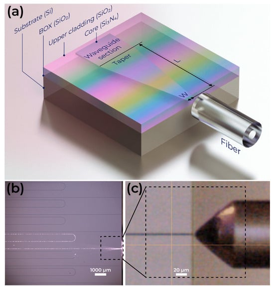
Figure 1.
(a) Three-dimensional visualization of fiber coupled to taper. (b) Light propagation through the waveguide. (c) Coupling of lensed fiber with chip facet.
Modeling started with the waveguide geometry determination to ensure fundamental mode excitation (Figure 2a). Modeling was carried out in Ansys Lumerical finite-difference eigenmode (FDE), based on which a waveguide width of 1200 nm was chosen. The fundamental mode excited in the waveguide with 220 × 1200 nm cross-section is shown in Figure 2b.
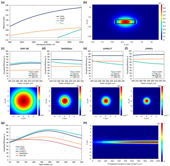
Figure 2.
(a) Calculation of Si3N4 effective index of modes excited in a waveguide as a function of waveguide width. (b) Fundamental mode excited in the waveguide with 220 × 1200 nm cross-section. ((c–f), top) Calculation of the taper length at different widths for different fiber types with wavelength 1550 nm. ((c–f), bottom) Optical mode field distribution at the light-source facet with different fiber types. (g) Calculation of the taper width with fixed length of taper (360 µm) for different fiber types with wavelength 1550 nm. (h) Mode propagation in the on-chip taper under lensed-fiber excitation.
To determine the optimal taper geometry, modeling was performed in Ansys Lumerical finite-difference time-domain (FDTD) based on the numerical solution of Maxwell’s equations. The length of the tapers varied from 200 µm to 520 µm. In its turn, the width at the beginning of the taper varied from 50 to 500 nm and was increased to the waveguide width value of 1200 nm. The smallest feature size, which we used in the modeling, is determined by the technological capabilities of electron lithography-based fabrication technology. The graphs (Figure 2c–f (top)) show the dependence obtained during the simulation for the different optical fibers. In this study, the taper length was chosen to be 360 μm to ensure low losses and a relatively small device footprint. To standardize the technological process, a taper geometry (width 280 nm, length 360 µm) was chosen to provide high coupling efficiency for all types of optical fibers (Figure 2g). Figure 2c–f (bottom), reports the optical mode field distributions at the light-source facet for representative fiber types (SMF-28, SM1500es, UHNA-7, and a Lensed fiber). In all field maps in Figure 2c–f (bottom), only the fundamental mode (TE0) at the light-source facet is shown. In Figure 2h, the simulated map shows the mode propagation inside the on-chip taper. The excitation is the focused output of a lensed fiber, represented as a Gaussian source at the chip facet.
2.2. Coupling Efficiency Improvement
Another approach to improve coupling efficiency is to use thicker cladding and a thicker bottom SiO2 layer, which mitigate vertical mode mismatch and reflections from the Si, respectively. Compared designs in Figure 3: inverse taper (width 280 nm; length 360 µm; BOX + Clad: 2.5 + 2.5; 4 + 4 µm) and multi-tip taper (tip 220 µm; start 100 nm; connection 5 µm; taper 40 µm; BOX + Clad: 4 + 4 µm) under SMF-28 excitation.
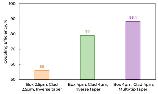
Figure 3.
Simulated coupling efficiency versus SiO2 thickness and taper type.
2.3. Multi-Tip Taper Simulation
One of the possible ways to reduce coupling losses is to use a multi-tip taper. Improving the geometry of the edge couplers by increasing the tip number often makes improvements to the coupling performance between optical fiber and optical channel on chip [50].
For example, for SMF-28 fiber mode, the field diameter is 10 μm, so a wide taper will allow the capture of more optical power from the fiber. And the multi-tip (trident-shape) taper will reduce the mismatch of the effective indices of the fiber and of the chip waveguide. Here we propose the multi-taper design for the SMF-28 fiber. Its design consists of three sections (Figure 4): a trident, a transition region, and an adiabatic taper. The tip length, tip start width, connection length, and taper length with the highest coupling efficiency are calculated by Ansys Lumerical FDTD. The results are shown in Figure 4. The chosen geometry of multi-taper has the following parameters: tip length = 220 µm, tip start width = 100 nm, connection length = 5 µm, and taper length = 40 µm. The calculated coupling losses with such multi-taper for SMF-28 fiber were improved from 2.52 to 0.51 dB.
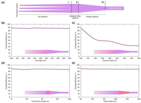
Figure 4.
(a) Visualization of multi-tip taper parts. (b) Calculation of the tip length for multi-tip taper. (c) Calculation of the tip start width for multi-tip taper. (d) Calculation of the connection length for multi-tip taper. (e) Calculation of the taper length for multi-tip taper.
We additionally present the optical mode field distribution at the start of the multi-tip taper (Figure 5a) and at start of the waveguide (Figure 5c), together with the field transition along the propagation direction of the multi-tip taper (Figure 5d). The longitudinal map (Figure 5d) shows a smooth, adiabatic evolution without standing-wave features, indicating robust recombination of the three tips with low phase sensitivity. The wavelength-dependent coupling efficiency within 1500–1600 nm (Figure 5b) remains in the 87–88.6% range. The small variation evidences broadband and spectrally stable performance of the multi-tip taper.
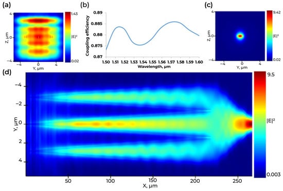
Figure 5.
Simulation and spectral performance of the multi-tip taper. (a) Optical mode field distribution at the start of the multi-tip taper. (b) Wavelength-dependent coupling efficiency in the 1500–1600 nm range. (c) Optical mode field distribution at the start of the waveguide after the taper end. (d) Optical mode field transition along the longitudinal direction of the multi-tip taper.
3. Fabrication
Edge Facet
To provide high taper coupling efficiency, the PIC dies are typically polished to obtain high optical-grade quality edges [51]. Although this process works well with small chip sizes, its scaling up to wafer level is impractical. There is also used the process of silicon dioxide thick layers wet etching, but it is anisotropic, which negatively affects the quality of the optical facets [52]. Other solutions for PICs optical facets fabrication need to be investigated. A promising technology is the reactive plasma dicing [53]. In this work, a 4-inch (100 mm) Si wafer was used, and the chips were diced into 25 × 25 mm dies.
Current study continues the previous research dedicated to the near-infrared wavelength single-mode Si3N4 submicron waveguide platform (220 × 550 nm) [54] and presents a plasma-based process for optical-grade edge facets fabrication. The fabrication process of low-loss silicon nitride photonic integrated circuits with fiber coupling through edge couplers is shown in Figure 6. The presented technology is used to dice a chip that consists of a 220 nm-thick stoichiometric low-pressure chemical vapor Si3N4 layer grown on the 525-μm silicon substrate oxidized to the 2.5-μm oxide thickness and covered with 2.5-μm oxide. A standard sequence of basic operations is involved for fabrication (Figure 6). First, the waveguide structures and alignment marks were patterned using electron-beam lithography with ma-N 2403 resist and multipass exposure. The pattern is then transferred to the Si3N4 device layer by reactive ion plasma etching (RIE) [55] with subsequent resist removal step in the N-methyl-2-pyrrolidone (NMP) and Si3N4 active layer cleaning procedure. Afterwards, the PECVD cover oxide was deposited and furnace annealing was performed. After nanotopology patterning the chip is diced using the deep reactive ion etching (DRIE) of the SiO2–Si3N4–SiO2 layer and Bosch process of the Si layer. The dicing process consists of the following stages: surface preparation (O2-plasma activation), photoresist spin coating (SPR220), laser lithography, photoresist development (MF-24A), SiO2–Si3N4–SiO2 thin-film stack etching using fluorine gases, silicon etching by the Bosch process, and photoresist removal by soaking in acetone followed by an IPA rinse [55].
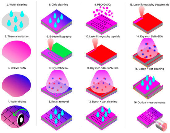
Figure 6.
Si3N4 PICs with edge coupling fabrication process.
In the multi-tip taper, the most critical electron-beam lithography dimensions are the tip width and the taper gaps, targeted at 100 nm. Following process development, scanning electron microscopy (SEM) confirmed a gap of 105 nm and a tip width of 140 nm (Figure 7).
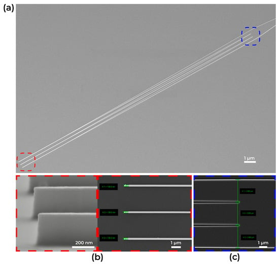
Figure 7.
(a) SEM image of multi-tip taper. ((b), red box) SEM image of multi-tip taper start tips. ((c), blue box) SEM image of gap between multi-tip taper end tips.
To fabricate a photonic integrated circuit with thick oxide layers by deep etching, it is necessary to use a thicker resist layer. The processes of 9.5 μm-thick resist spin-coating and its laser lithography were developed. The 89.0° resist sidewall angle corresponded to the following lithography regime: multipass-technology, 60 mW laser power, −25% focus. Figure 8 shows the resist profile angle after the laser lithography step and the profile angle of the optical layers after the etching steps.
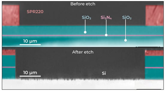
Figure 8.
Optical image of angle profile after laser lithography (top) and after dry etch process (bottom).
4. Characterization
4.1. Cut-Back Measurement
To measure the I/O efficiency, we used an automated assembly system equipped with a 12-axis alignment drive (5 nm resolution), a wavelength-stabilized 1550 nm laser source and an optical power meter. This system made it possible to measure internal optical losses and coupling efficiency using the output power values of structures of various lengths.
The cut-back propagation loss analysis [56,57] in the fabricated Si3N4 waveguides was performed for specially designed PIC chips. Propagation losses were measured for the test structure with three different lengths (2, 3, and 4 cm). Measurement setup is shown in Figure 9a. Figure 9b presents the measured losses for different fiber types and different SiO2 layers thickness. The light was coupled out from the polished fiber array unit (FAU) through PIC to the power detector.
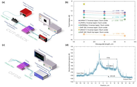
Figure 9.
(a) Schematic of the measurement setup for cut-back characterization. (b) Propagation losses measured by the cut-back, calculated by y = k × x + b where k = propagation losses and b = coupling losses for wavelength 1550 nm. (c) Schematic of the measurement setup for OFDR characterization. (d) OFDR characterization along the waveguide. The dashed line shows the linear fit of the waveguide reflections.
The lowest coupling losses for the inverse taper of 0.81 dB (violet line in Figure 9b, 0.81 = 1.62/2 dB) were observed for the UHNA-7 fiber. For the device with increased cladding oxide thickness (Figure 9b, star), the measured total insertion loss was = 0.66 dB at
= 2 cm, and the propagation loss from the cut-back fit was = 0.18 dB/cm. The total loss of a straight device is given by
where
is the coupling loss per facet. Substituting the measured values gives
4.2. OFDR Measurements
Cut-back measurements were cross-checked using a reflectometry technique. Reflectometry is widely used in fiber optics to probe the local reflectivity of waveguides and devices with respect to propagation distance [58]. Figure 9c shows schematic of the measurement setup for optical frequency domain reflectometry (OFDR) characterization. With a point-to-point resolution of about 10 µm and detection sensitivity of −130 dB over 30 m of propagation, coherent OFDR is a particularly useful technique in characterizing waveguides and devices at the planar scale [59,60]. In the OFDR, a continuous wave laser source is scanned over several terahertz in frequency or, equivalently, several tens of nanometers in wavelength. A larger scan range improves the measurement spatial resolution according to the following expression:
where Dmin is the minimum distance between the two data points, c is the speed of light, ng is the group index, fstart and λstart are the source frequency and wavelength at the scanning start, respectively, and fend and λend are the source frequency and wavelength at the scanning end [32]. However, all parameters derived from the spatial domain data are then averaged over the measurement scan spectral range. If the parameter spectral dependence is set, the rectangular window function can be applied to data in the spectral domain to narrow the included spectral range. This window could be moved across the measurement’s full spectral range, making it possible to extract the parameter at each window position and obtain the parameter spectral dependence from a single OFDR scan. Because narrowing data in the frequency domain decreases the measurement spatial resolution according to Equation (3), a tradeoff appears between the spectral averaging, which could distort the actual spectral dependence and the measurement accuracy. In this study, an FDTD window width of 10 nm is used to extract the spectrally dependent measurements of the coupling loss propagation loss.
Figure 9d shows the OFDR data from two UHNA-7 fibers coupled to waveguides (10 cm long). The data was not filtered in the spectral domain, and a moving average filter with 100-datapoint or ~1 mm window size was applied in the spatial domain to reduce the backscatter amplitude deviation. Before OFDR scanning, fiber-to-chip coupling was maximized using an OFDR source laser and an optical power meter. In Figure 9d, the horizontal dashed lines indicate the total loss across the device (input coupling + waveguide + output coupling), while the dashed sloped line represents the linear fit from which the waveguide propagation loss (dB/cm) is obtained. The difference between these two levels of 5.96 dB includes the total return loss between the two fibers, or,
where
is the total return loss in dB,
is the total insertion loss,
is the fiber-to-chip insertion loss per facet, and
is the total propagation insertion loss.
The measured data is linearly fitted to find propagation losses (Figure 9d). Based on OFDR characterization, the propagation insertion loss is 0.13 dB/cm and fiber-to-chip insertion loss per facet is 0.84 dB. That corresponds well to the results obtained with cut-back measurements: coupling losses of 0.81 dB and propagation losses of 0.18 dB/cm (violet line in Figure 9b).
5. Discussion
This study presents a universal strategy for repeatable wafer-scale PIC low-loss edge coupling. Here we provide a tutorial on the design, manufacturing, and characterization of lithographically defined optical coupling facets using an ICP dry etching technique. We also designed, fabricated, and experimentally validated inverse and multi-tip taper for UHNA-7 and SMF-28 fibers.
The coupling geometries were optimized using numerical simulations based on FDE and FDTD methods. The waveguide cross-section was first selected to ensure robust single-mode operation, after which the taper length and tip width were varied to achieve adiabatic mode transformation for different fiber types. The simulations indicate that a taper length of approximately 360 μm offers a favorable trade-off between coupling efficiency and device footprint, while remaining compatible with electron-beam lithography constraints. The optimized design offers calculated coupling losses for UHNA-7 fiber at the level of ∼0.10 dB and for SMF-28 fiber at the level of ∼0.50 dB be for 1550 nm per facet. To address the strong mode mismatch for standard SMF-28 fibers, a multi-tip (trident-shaped) taper was introduced, enabling a smoother modal transition by redistributing the optical field among several narrow tips. The chosen geometry of multi-taper has the following parameters: tip length = 220 µm, tip start width = 100 nm, connection length = 5 µm, and taper length = 40 µm. The optimized multi-tip design exhibits a marked reduction in calculated coupling losses and maintains stable performance over the 1500–1600 nm wavelength range and calculated coupling losses with such multi-taper for SMF-28 fiber were improved from 2.52 to 0.51 dB.
The proposed coupling structures were fabricated using a wafer-scale Si3N4 photonic process incorporating DRIE-based plasma dicing. This approach enables the formation of optical-grade facets without mechanical polishing, thereby improving reproducibility and scalability. Inverse tapers and multi-tip structures were defined by electron-beam lithography, with critical feature sizes approaching 100 nm. Scanning electron microscopy confirmed good agreement between the designed and fabricated dimensions. Fabrication process optimization allowed us to obtain the 89° optical-grade facet, which is essential for minimizing scattering and reflection losses during fiber-to-chip coupling.
Device performance was characterized using cut-back measurements and OFDR. OFDR measurements independently verified the extracted coupling and propagation losses and showed good consistency with the cut-back analysis. When interfacing with SMF-28 fibers, the multi-tip taper demonstrated a measured coupling loss of approximately 1.5 dB per facet, confirming the effectiveness of the proposed design in mitigating mode mismatch. The best coupling losses of 0.15 dB were achieved for the UHNA-7 fiber with single-mode Si3N4 waveguide (220 × 1200 nm), that agrees well with the simulation results.
Author Contributions
I.A.R. and A.S.B. conceptualized the ideas of the project. S.S.A., E.V.S., A.B.K., A.V.B., K.A.B., S.V.B. and D.A.B. fabricated experimental samples and discussed results. S.S.A., A.B.K., A.V.B., D.V.K. and K.A.B. modeled the optical elements. S.S.A., A.S.B., A.B.K., A.V.B. and D.A.B. developed the edge facet fabrication process. S.S.A., K.A.B., A.S.L., V.V.E., A.S.A. and E.S.L. conducted the optical characterization of the experimental samples. S.S.A., A.S.B., K.A.B. and I.A.R. analyzed the experimental data and discussed the results. S.S.A., A.S.B., K.A.B. and I.A.S. prepared writing—original draft. I.A.R. reviewed and edited the manuscript. I.A.R. supervised the project. All authors have read and agreed to the published version of the manuscript.
Funding
This research received no external funding.
Data Availability Statement
Data supporting the findings are available within the article and from the corresponding author upon reasonable request.
Acknowledgments
Technology was developed, and samples were fabricated and measured at Quantum Park (BMSTU Nanofabrication Facility, Shukhov Labs, FMNS REC, ID 74300).
Conflicts of Interest
The authors declare no conflicts of interest.
Abbreviations
The following abbreviations are used in this manuscript:
| UHNA | Ultra-High Numerical Aperture |
| PIC | Photonic integrated circuits |
| QKD | Quantum key distribution |
| SOI | Silicon-on-insulator |
| MPW | Multi-Project Wafer |
| DUV | Deep ultraviolet |
| FDE | Finite-difference eigenmode |
| FDTD | Finite-difference time-domain |
| FAU | Fiber array unit |
| DRIE | Deep reactive ion plasma etching |
| RIE | Reactive ion plasma etching |
| ICP | Inductively Coupled Plasma |
| OFDR | Optical frequency domain reflectometry |
| SMF | Single-Mode Fiber |
References
- Malhouitre, S.; Fowler, D.; Garcia, S.; Lemonnier, O.; Tyler, N.; Rabaud, W. Silicon nitride photonic platform for LiDAR applications. In Proceedings of the 2018 IEEE 15th International Conference on Group IV Photonics (GFP), Cancun, Mexico, 29–31 August 2018; IEEE: New York, NY, USA, 2018; pp. 1–2. [Google Scholar]
- Rodionov, I.A.; Baburin, A.S.; Zverev, A.V.; Philippov, I.A.; Gabidulin, A.R.; Dobronosova, A.A.; Ryzhova, E.V.; Vinogradov, A.P.; Ivanov, A.I.; Maklakov, S.S.; et al. Mass-production compatible fabrication techniques of single-crystalline silver metamaterials and plasmonic devices. In Metamaterials, Metadevices, and Metasystems 2017; Engheta, N., Noginov, M.A., Zheludev, N.I., Eds.; SPIE: Bellingham, WA, USA, 2017; Volume 10343, p. 1034337. [Google Scholar]
- Baburin, A.S.; Ivanov, A.; Trofimov, I.; Dobronosova, A.; Melentiev, P.; Balykin, V.; Moskalev, D.; Pishchimova, A.; Ganieva, L.; Ryzhikov, I.; et al. Highly directional plasmonic nanolaser based on high-performance noble metal film photonic crystal. In Nanophotonics VII; SPIE: Bellingham, WA, USA, 2018; p. 159. [Google Scholar]
- Yankovskii, G.M.; Komarov, A.V.; Puz’ko, R.S.; Baryshev, A.V.; Afanas’ev, K.N.; Boginskaya, I.A.; Bykov, I.V.; Merzlikin, A.M.; Rodionov, I.A.; Ryzhikov, I.A. Structural and optical properties of single and bilayer silver and gold films. Phys. Solid State 2016, 58, 2503–2510. [Google Scholar] [CrossRef]
- Baburin, A.S.; Ivanov, A.I.; Ryzhikov, I.A.; Trofimov, I.V.; Gabidullin, A.R.; Moskalev, D.O.; Panfilov, Y.V.; Rodionov, I.A. Crystalline structure dependence on optical properties of silver thin film over time. In Proceedings of the 2017 Progress in Electromagnetics Research Symposium (PIERS), St. Petersburg, Russia, 22–25 May 2017; IEEE: New York, NY, USA, 2017; pp. 1497–1502. [Google Scholar]
- Baburin, A.S.; Moskalev, D.O.; Lotkov, E.S.; Sorokina, O.S.; Baklykov, D.A.; Avdeev, S.S.; Buzaverov, K.A.; Yankovskii, G.M.; Baryshev, A.V.; Ryzhikov, I.A.; et al. Evolutionary selection growth of silver films for low-loss nanophotonic devices. Surf. Interfaces 2023, 39, 102897. [Google Scholar] [CrossRef]
- Lagarkov, A.; Boginskaya, I.; Bykov, I.; Budashov, I.; Ivanov, A.; Kurochkin, I.; Ryzhikov, I.; Rodionov, I.; Sedova, M.; Zverev, A.; et al. Light localization and SERS in tip-shaped silicon metasurface. Opt. Express 2017, 25, 17021–17038. [Google Scholar] [CrossRef] [PubMed]
- Hoi, H.; Rezaie, S.S.; Gong, L.; Sen, P.; Zeng, H.; Montemagno, C.; Gupta, M. Biofunctionalized silicon nitride platform for sensing applications. Biosens. Bioelectron. 2018, 102, 497–503. [Google Scholar] [CrossRef]
- Lotkov, E.S.; Baburin, A.S.; Ryzhikov, I.A.; Sorokina, O.S.; Ivanov, A.I.; Zverev, A.V.; Ryzhkov, V.V.; Bykov, I.V.; Baryshev, A.V.; Panfilov, Y.V.; et al. ITO film stack engineering for low-loss silicon optical modulators. Sci. Rep. 2022, 12, 14902. [Google Scholar] [CrossRef]
- Stepanov, I.A.; Baburin, A.S.; Kushnev, D.V.; Sergeev, E.V.; Shmonina, O.I.; Matanin, A.R.; Echeistov, V.V.; Ryzhikov, I.A.; Panfilov, Y.V.; Rodionov, I.A. Sputtered NbN films for ultra-high performance superconducting nanowire single-photon detectors. APL Mater. 2024, 12, 021101. [Google Scholar] [CrossRef]
- Taballione, C.; Wolterink, T.A.W.; Lugani, J.; Eckstein, A.; Bell, B.A.; Grootjans, R.; Visscher, I.; Geskus, D.; Roeloffzen, C.G.H.; Renema, J.J.; et al. 8 × 8 reconfigurable quantum photonic processor based on silicon nitride waveguides. Opt. Express 2019, 27, 26842–26857. [Google Scholar] [CrossRef]
- Weng, H.-C.; Monroy-Ruz, J.; Matthews, J.C.F.; Rarity, J.G.; Balram, K.C.; Smith, J.A. Heterogeneous integration of solid-state quantum systems with a foundry photonics platform. ACS Photonics 2023, 10, 3302–3309. [Google Scholar] [CrossRef]
- Xiang, C.; Jin, W.; Bowers, J.E. Silicon nitride passive and active photonic integrated circuits: Trends and prospects. Photonics Res. 2022, 10, A82–A96. [Google Scholar] [CrossRef]
- Guo, X.; Ji, X.; Yao, B.; Tan, T.; Chu, A.; Westreich, O.; Dutt, A.; Wong, C.; Su, Y. Ultra-wideband integrated photonic devices on silicon platform: From visible to mid-IR. Nanophotonics 2023, 12, 167–196. [Google Scholar] [CrossRef]
- Baets, R.; Subramanian, A.Z.; Clemmen, S.; Kuyken, B.; Bienstman, P.; Le Thomas, N.; Roelkens, G.; Van Thourhout, D.; Helin, P.; Severi, S. Silicon photonics: Silicon nitride versus silicon-on-insulator. In Proceedings of the Optical Fiber Communication Conference, Anaheim, CA, USA, 20–22 March 2016; OSA: Washington, DC, USA, 2016. [Google Scholar]
- Muñoz, P.; Micó, G.; Bru, L.; Pastor, D.; Pérez, D.; Doménech, J.; Fernández, J.; Baños, R.; Gargallo, B.; Alemany, R.; et al. Silicon nitride photonic integration platforms for visible, near-infrared and mid-infrared applications. Sensors 2017, 17, 2088. [Google Scholar] [CrossRef] [PubMed]
- Ben Bakir, B.; de Gyves, A.V.; Orobtchouk, R.; Lyan, P.; Porzier, C.; Roman, A.; Fedeli, J.-M. Low-loss (<1 dB) and polarization-insensitive edge fiber couplers fabricated on 200-mm silicon-on-insulator wafers. IEEE Photonics Technol. Lett. 2010, 22, 739–741. [Google Scholar] [CrossRef]
- Hatori, N.; Shimizu, T.; Okano, M.; Ishizaka, M.; Yamamoto, T.; Urino, Y.; Mori, M.; Nakamura, T.; Arakawa, Y. A hybrid integrated light source on a silicon platform using a trident spot-size converter. J. Light. Technol. 2014, 32, 1329–1336. [Google Scholar] [CrossRef]
- Urino, Y.; Usuki, T.; Fujikata, J.; Ishizaka, M.; Yamada, K.; Horikawa, T.; Nakamura, T.; Arakawa, Y. High-density and wide-bandwidth optical interconnects with silicon optical interposers [Invited]. Photonics Res. 2014, 2, A1–A10. [Google Scholar] [CrossRef]
- Cheben, P.; Schmid, J.H.; Wang, S.; Xu, D.-X.; Vachon, M.; Janz, S.; Lapointe, J.; Painchaud, Y.; Picard, M.-J. Broadband polarization-independent nanophotonic coupler for silicon waveguides with ultra-high efficiency. Opt. Express 2015, 23, 22553–22563. [Google Scholar] [CrossRef]
- Papes, M.; Cheben, P.; Benedikovic, D.; Schmid, J.H.; Pond, J.; Halir, R.; Ortega-Moñux, A.; Wangüemert-Pérez, G.; Ye, W.N.; Xu, D.-X.; et al. Fiber–chip edge coupler with large mode size for silicon photonic wire waveguides. Opt. Express 2016, 24, 5026–5038. [Google Scholar] [CrossRef]
- Atsumi, Y.; Yoshida, T.; Omoda, E.; Sakakibara, Y. Broadband surface optical coupler based on a SiO2-capped vertically curved silicon waveguide. Opt. Express 2018, 26, 10400–10408. [Google Scholar] [CrossRef]
- Shoji, T.; Tsuchizawa, T.; Watanabe, K.; Yamada, K.; Morita, H. Low loss mode size converter from 0.3 μm square Si wire waveguides to single mode fibres. Electron. Lett. 2002, 38, 1669–1670. [Google Scholar] [CrossRef]
- Almeida, V.R.; Panepucci, R.R.; Lipson, M. Nanotaper for compact mode conversion. Opt. Lett. 2003, 28, 1302–1304. [Google Scholar] [CrossRef]
- Roelkens, G.; Dumon, P.; Bogaerts, W.; Van Thourhout, D.; Baets, R. Efficient silicon-on-insulator fiber coupler fabricated using 248-nm deep UV lithography. IEEE Photonics Technol. Lett. 2005, 17, 2613–2615. [Google Scholar] [CrossRef]
- McNab, S.; Moll, N.; Vlasov, Y. Ultra-low loss photonic integrated circuit with membrane-type photonic crystal waveguides. Opt. Express 2003, 11, 2927–2939. [Google Scholar] [CrossRef] [PubMed]
- Marchetti, R.; Lacava, C.; Carroll, L.; Gradkowski, K.; Minzioni, P. Coupling strategies for silicon photonics integrated chips [Invited]. Photonics Res. 2019, 7, 201–239. [Google Scholar] [CrossRef]
- Zhu, Y.; Wang, J.; Xie, W.; Tian, B.; Li, Y.; Brainis, E.; Jiao, Y.; Van Thourhout, D. Ultra-compact silicon nitride grating coupler for microscopy systems. Opt. Express 2017, 25, 33297–33305. [Google Scholar] [CrossRef]
- Mak, J.C.C.; Sacher, W.D.; Ying, H.; Luo, X.; Lo, P.G.-Q.; Poon, J.K.S. Multi-layer silicon nitride-on-silicon polarization-independent grating couplers. Opt. Express 2018, 26, 30623–30633. [Google Scholar] [CrossRef]
- Son, G.; Han, S.; Park, J.; Kwon, K.; Yu, K. High-efficiency broadband light coupling between optical fibers and photonic integrated circuits. Nanophotonics 2018, 7, 1845–1864. [Google Scholar] [CrossRef]
- Mitomi, O.; Kasaya, K.; Miyazawa, H. Design of a single-mode tapered waveguide for low-loss chip-to-fiber coupling. IEEE J. Quantum Electron. 1994, 30, 1787–1793. [Google Scholar] [CrossRef]
- Zou, J.; Yu, Y.; Ye, M.; Liu, L.; Deng, S.; Xu, X.; Zhang, X. Short and efficient mode-size converter designed by segmented-stepwise method. Opt. Lett. 2014, 39, 6273–6276. [Google Scholar] [CrossRef] [PubMed]
- Mizuno, T.; Kitoh, T.; Ishii, M.; Inoue, Y.; Saida, T.; Itoh, M.; Shibata, T.; Hibino, Y. Compact and low-loss arrayed waveguide grating module with tolerance-relaxed spot-size converter. IEEE Photonics Technol. Lett. 2003, 15, 239–241. [Google Scholar] [CrossRef]
- Liu, Y.; Sun, W.; Xie, H.; Zhang, N.; Xu, K.; Yao, Y.; Xiao, S.; Song, Q. Adiabatic and ultracompact waveguide tapers based on digital metamaterials. IEEE J. Sel. Top. Quantum Electron. 2019, 25, 1–6. [Google Scholar] [CrossRef]
- Tao, H.; Song, J.; Fang, Q.; Yu, M.; Lo, G.; Kwong, D. Improving coupling efficiency of fiber–waveguide coupling with a double-tip coupler. Opt. Express 2008, 16, 20803–20810. [Google Scholar] [CrossRef]
- Kohli, N.; Ménard, M.; Ye, W.N. Efficient TE/TM spot-size converter for broadband coupling to single-mode fibers. OSA Contin. 2019, 2, 2428–2441. [Google Scholar] [CrossRef]
- Zhu, T.; Hu, Y.; Gatkine, P.; Veilleux, S.; Bland-Hawthorn, J.; Dagenais, M. Ultrabroadband high coupling efficiency fiber-to-waveguide coupler using Si3N4/SiO2 waveguides on silicon. IEEE Photonics J. 2016, 8, 1–12. [Google Scholar]
- Sethi, P.; Kallega, R.; Haldar, A.; Selvaraja, S.K. Compact broadband low-loss taper for coupling to a silicon nitride photonic wire. Opt. Lett. 2018, 43, 3433–3436. [Google Scholar] [CrossRef] [PubMed]
- Fernández, J.; Baños, R.; Doménech, D.; Domínguez, C.; Muñoz, P. Low-loss inverted taper edge coupler in silicon nitride. IET Optoelectron. 2019, 13, 62–66. [Google Scholar] [CrossRef]
- Wang, Y.; Xu, L.; Yun, H.; Ma, M.; Kumar, A.; El-Fiky, E.; Li, R.; Abadiacalvo, N.; Chrostowski, L.; Jaeger, N.A.F.; et al. Polarization-independent mode-evolution-based coupler for the silicon-on-insulator platform. IEEE Photonics J. 2018, 10, 1–10. [Google Scholar] [CrossRef]
- Xu, L.; Wang, Y.; Kumar, A.; El-Fiky, E.; Mao, D.; Tamazin, H.; Jacques, M.; Xing, Z.; Saber, M.d.G.; Plant, D.V. Compact high-performance adiabatic 3-dB coupler enabled by subwavelength-grating slot in the silicon-on-insulator platform. Opt. Express 2018, 26, 29873–29884. [Google Scholar] [CrossRef]
- Yun, H.; Chrostowski, L.; Jaeger, N.A.F. Ultra-broadband 2 × 2 adiabatic 3-dB coupler using subwavelength-grating-assisted silicon-on-insulator strip waveguides. Opt. Lett. 2018, 43, 1935–1938. [Google Scholar] [CrossRef]
- Mao, D.; Alam, M.S.; Zhang, J.; Zhu, M.; Koh, P.-C.; Plant, D.V.; Wang, Y.; El-Fiky, E.; Xu, L.; Kumar, A.; et al. Adiabatic coupler with design-intended splitting ratio. J. Light. Technol. 2019, 37, 6147–6155. [Google Scholar] [CrossRef]
- Fu, Y.; Ye, T.; Tang, W.; Chu, T. Efficient adiabatic silicon-on-insulator waveguide taper. Photonics Res. 2014, 2, A41–A45. [Google Scholar] [CrossRef]
- Pu, M.; Liu, L.; Ou, H.; Yvind, K.; Hvam, J.M. Ultra-low-loss inverted taper coupler for silicon-on-insulator ridge waveguide. Opt. Commun. 2010, 283, 3678–3682. [Google Scholar] [CrossRef]
- Tobing, L.Y.M.; Cao, Y.; Lau, C.; Tong, A.S.K.; Lee, S.H.J.; Tsang, Y.F.; Goh, J.S.; Toh, Y.T.; Luo, X. Compact edge coupler with <1 dB/facet insertion loss in the C-band. In Integrated Optics: Devices, Materials, and Technologies XXIX; SPIE: Bellingham, WA, USA, 2025; Volume 13369, p. 1336907. [Google Scholar]
- Hettrick, S.J.; Wang, J.; Li, C.; Wilkinson, J.S.; Shepherd, D.P. An experimental comparison of linear and parabolic tapered waveguide lasers and a demonstration of broad-stripe diode pumping. J. Light. Technol. 2004, 22, 845–849. [Google Scholar] [CrossRef]
- Bhandari, B.; Im, C.-S.; Lee, K.-P.; Kim, S.-M.; Oh, M.-C.; Lee, S.-S. Compact and broadband edge coupler based on multi-stage silicon nitride tapers. IEEE Photonics J. 2020, 12, 1–11. [Google Scholar] [CrossRef]
- PsiQuantum Team. A manufacturable platform for photonic quantum computing. Nature 2025, 641, 876–883. [Google Scholar] [CrossRef]
- He, A.; Guo, X.; Wang, T.; Su, Y. Ultracompact fiber-to-chip metamaterial edge coupler. ACS Photonics 2021, 8, 3226–3233. [Google Scholar] [CrossRef]
- Fedeli, J.M.; Orobtchouk, R.; Seassal, C.; Vivien, L. Integration issues of a photonic layer on top of a CMOS circuit. In Silicon Photonics; SPIE: Bellingham, WA, USA, 2006; p. 61250H. [Google Scholar]
- Konstantinova, T.G.; Andronic, M.M.; Baklykov, D.A.; Stukalova, V.E.; Ezenkova, D.A.; Zikiy, E.V.; Bashinova, M.V.; Solovev, A.A.; Lotkov, E.S.; Ryzhikov, I.A.; et al. Deep multilevel wet etching of fused silica glass microstructures in BOE solution. Sci. Rep. 2023, 13, 5228. [Google Scholar] [CrossRef]
- Schnarrenberger, M.; Zimmermann, L.; Mitze, T.; Bruns, J.; Petermann, K. Facet preparation of SOI waveguides by etching and cleaving compared to dicing and polishing. In Proceedings of the First IEEE International Conference on Group IV Photonics (GFP 2004), Hong Kong, China, 29 September–1 October 2004; IEEE: New York, NY, USA, 2004; pp. 72–74. [Google Scholar]
- Buzaverov, K.A.; Baburin, A.S.; Sergeev, E.V.; Avdeev, S.S.; Lotkov, E.S.; Andronic, M.; Stukalova, V.E.; Baklykov, D.A.; Dyakonov, I.V.; Skryabin, N.N.; et al. Low-loss silicon nitride photonic ICs for near-infrared wavelength bandwidth. Opt. Express 2023, 31, 16227–16242. [Google Scholar] [CrossRef]
- Baklykov, D.A.; Andronic, M.; Sorokina, O.S.; Avdeev, S.S.; Buzaverov, K.A.; Ryzhikov, I.A.; Rodionov, I.A. Self-controlled cleaving method for silicon DRIE process cross-section characterization. Micromachines 2021, 12, 534. [Google Scholar] [CrossRef]
- Liao, Z.; Aitchison, J.S. Precision etching for multi-level AlGaAs waveguides. Opt. Mater. Express 2017, 7, 895–903. [Google Scholar] [CrossRef]
- Sacher, W.D.; Luo, X.; Yang, Y.; Chen, F.-D.; Lordello, T.; Mak, J.C.C.; Liu, X.; Hu, T.; Xue, T.; Lo, P.G.-Q.; et al. Visible-light silicon nitride waveguide devices and implantable neurophotonic probes on thinned 200-mm silicon wafers. Opt. Express 2019, 27, 37400–37418. [Google Scholar] [CrossRef] [PubMed]
- Soller, B.J.; Gifford, D.K.; Wolfe, M.S.; Froggatt, M.E. High-resolution optical frequency-domain reflectometry for characterization of components and assemblies. Opt. Express 2005, 13, 666–674. [Google Scholar] [CrossRef]
- Bauters, J.F.; Heck, M.J.R.; John, D.; Dai, D.; Tien, M.-C.; Barton, J.S.; Leinse, A.; Heideman, R.G.; Blumenthal, D.J.; Bowers, J.E. Ultra-low-loss high-aspect-ratio Si3N4 waveguides. Opt. Express 2011, 19, 3163–3174. [Google Scholar] [CrossRef] [PubMed]
- Glombitza, U.; Brinkmeyer, E. Coherent frequency-domain reflectometry for characterization of single-mode integrated-optical waveguides. J. Light. Technol. 1993, 11, 1377–1384. [Google Scholar] [CrossRef]
Disclaimer/Publisher’s Note: The statements, opinions and data contained in all publications are solely those of the individual author(s) and contributor(s) and not of MDPI and/or the editor(s). MDPI and/or the editor(s) disclaim responsibility for any injury to people or property resulting from any ideas, methods, instructions or products referred to in the content. |
© 2025 by the authors. Licensee MDPI, Basel, Switzerland. This article is an open access article distributed under the terms and conditions of the Creative Commons Attribution (CC BY) license (https://creativecommons.org/licenses/by/4.0/).