
Design and Application of Memristive Balanced Ternary Univariate Logic Circuit

 , and
, and 
Abstract
:1. Introduction
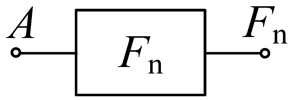
2. Balanced Ternary Univariate Logic Circuit
2.1. Three-State to Two-State Logic
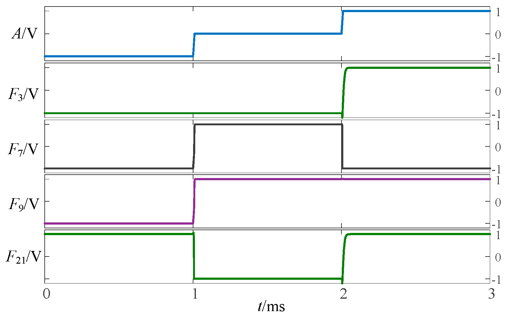
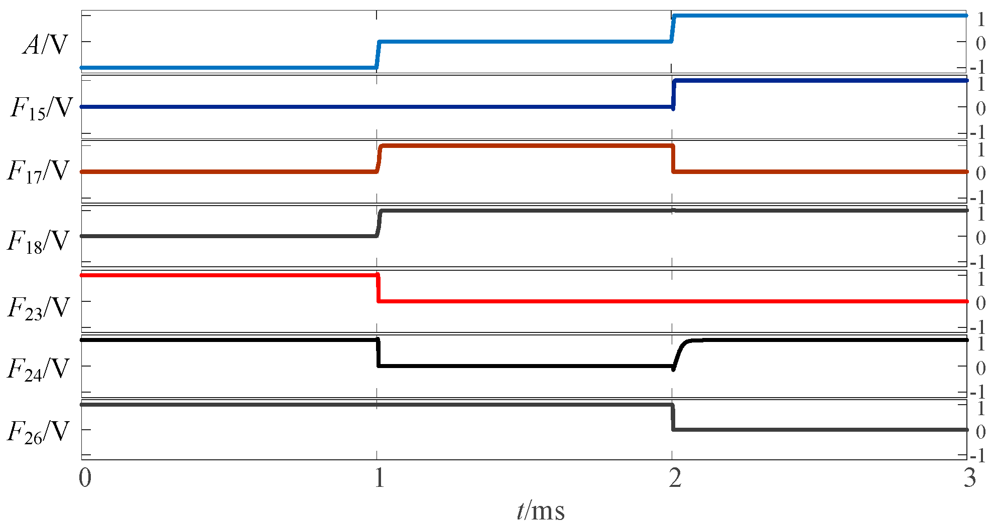
2.1.1. Circuit Design of Logic Function F4, F5, F9, F10, F13, F18, F23 and F26
2.1.2. The Circuit Design of the Remaining Three-State to Two-State Logic Function
2.1.3. Simulation Verification of Three-State to Two-State Logic Circuit
2.2. Three-State to Three-State Logic
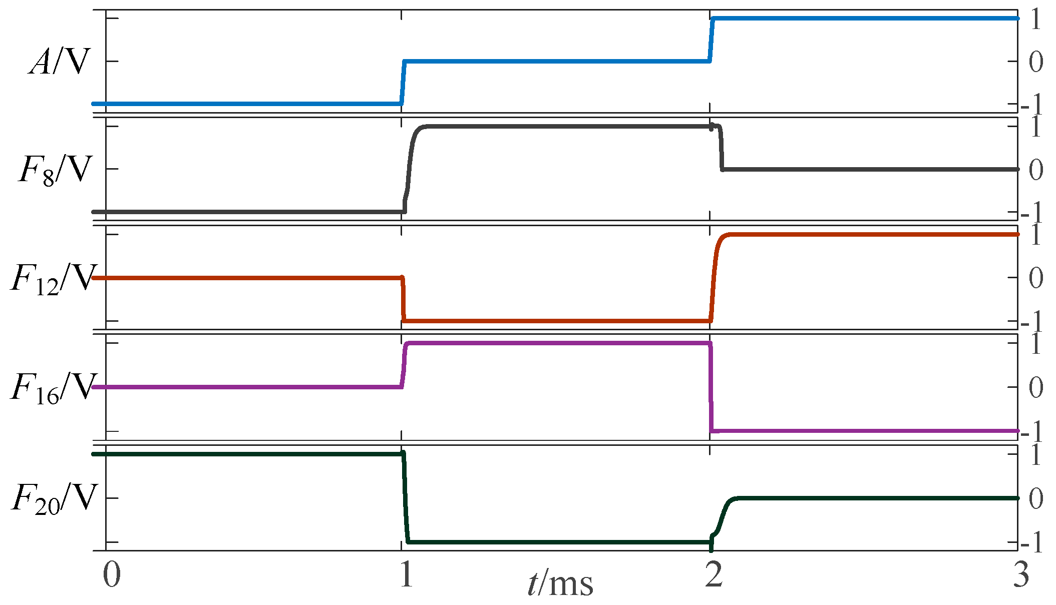
2.2.1. Circuit Design of Up-Spin Logic Function F16 and Down-Spin Logic Function F20
2.2.2. The Circuit Design of the Remaining Three-State to Three-State Logic Function
2.2.3. Verification of Three-State to Three-State Logic Circuit Using LTSpice Simulation
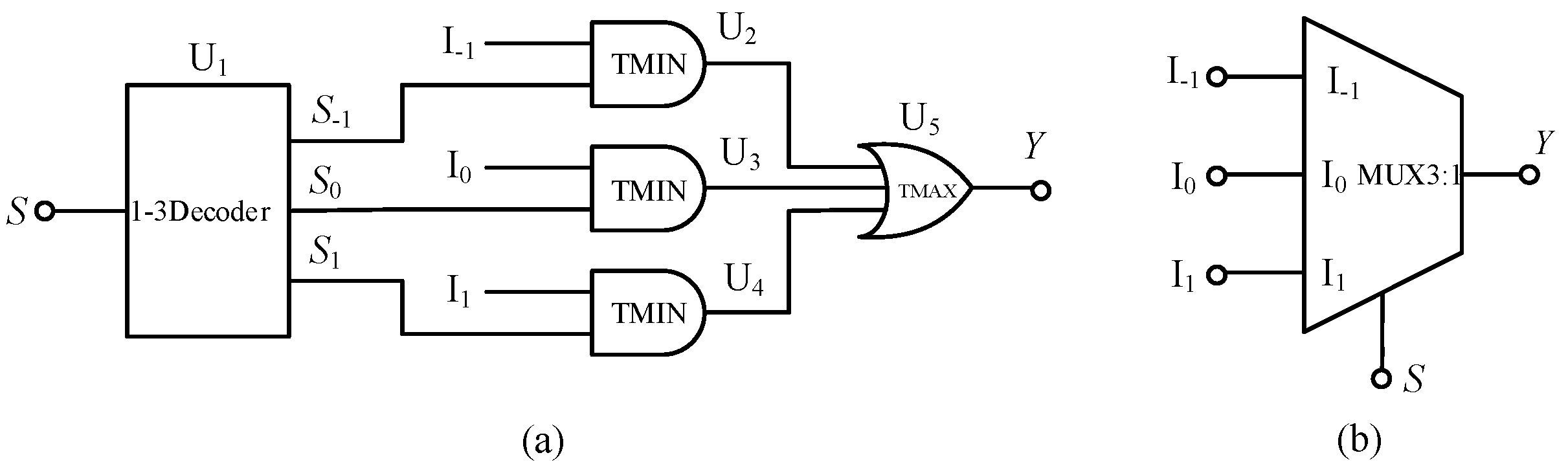
3. Design of Balanced Three-Valued Combinational Logic Circuit Based on Univariate Logic and Multiplexer
3.1. Balanced Ternary Half Adder
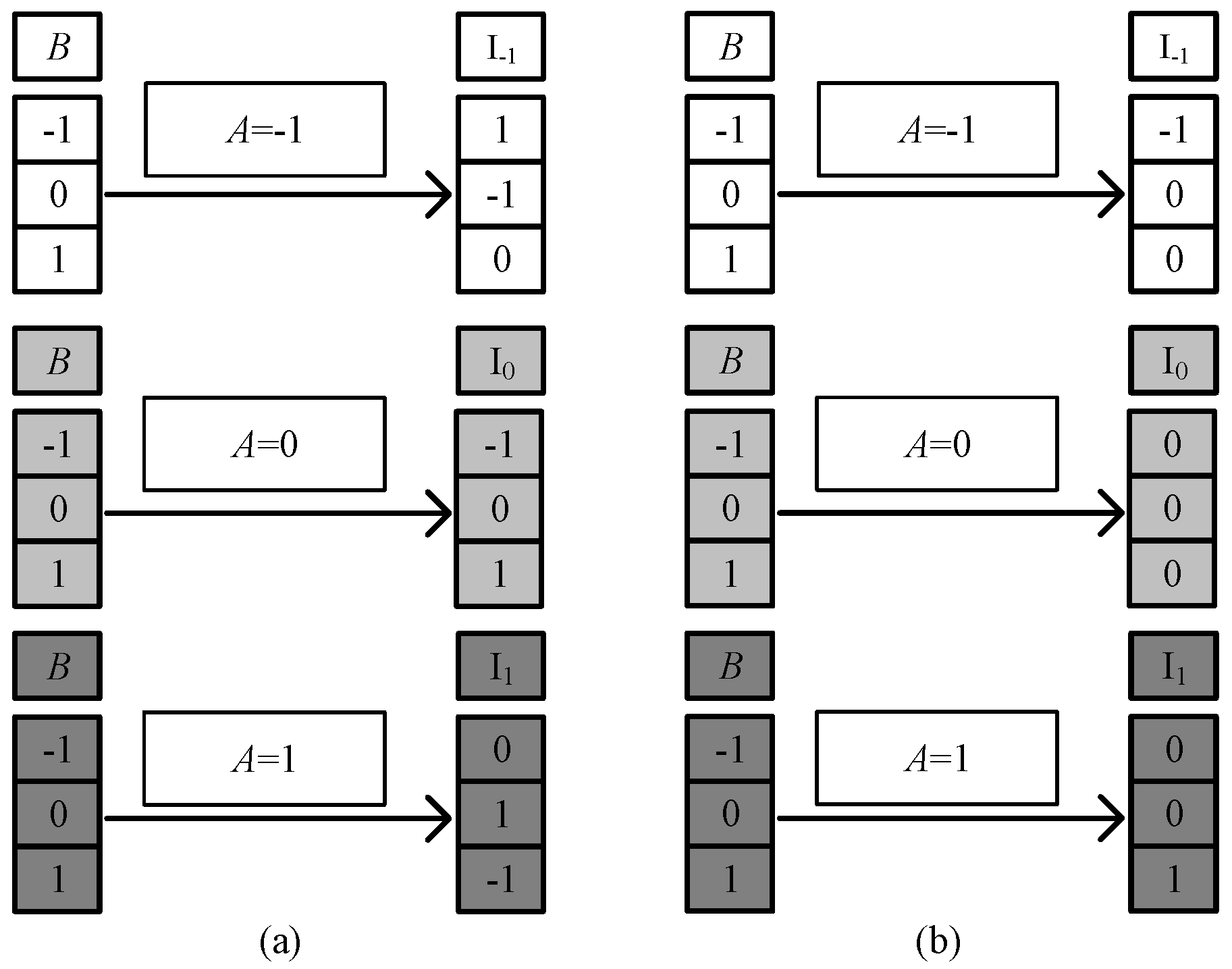
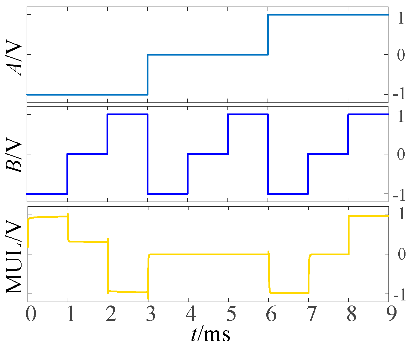
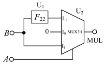
3.2. Balanced Ternary Multiplier
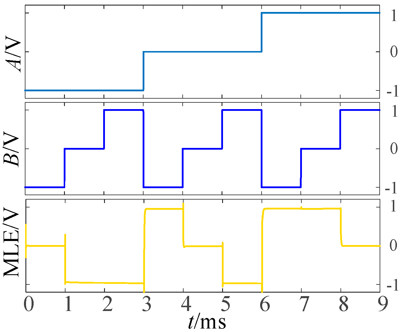
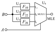
3.3. Balanced Ternary Numerical Comparator
4. Comparison and Analysis
5. Conclusions
Author Contributions
Funding
Data Availability Statement
Acknowledgments
Conflicts of Interest
References
- Kuhn, K.J. Considerations for ultimate CMOS scaling. IEEE Trans. Electron Devices 2012, 59, 1813–1828. [Google Scholar] [CrossRef]
- Wang, X.Y.; Dong, C.T.; Wu, Z.R.; Cheng, Z.Q. A review on the design of ternary logic circuits. Chin. Phys. B 2021, 30, 128402. [Google Scholar] [CrossRef]
- Sandhie, Z.T.; Ahmed, F.U.; Chowdhury, M.H. Design of ternary logic and arithmetic circuits using GNRFET. IEEE Open J. Nanotechnol. 2020, 1, 77–87. [Google Scholar] [CrossRef]
- Karmakar, S.; Chandy, J.A.; Jain, F.C. Design of ternary logic combinational circuits based on quantum dot gate FETS. IEEE Trans. Very Large Scale Integr. (VLSI) Syst. 2013, 21, 793–806. [Google Scholar] [CrossRef]
- Yang, J.; Lee, H.; Jeong, J.H.; Kim, T.; Lee, S.H.; Song, T. Circuit-level exploration of ternary logic using memristors and MOSFETs. IEEE Trans. Circuits Syst. I Regul. Pap. 2021, 69, 707–720. [Google Scholar] [CrossRef]
- Wang, X.Y.; Wu, Z.R.; Zhou, P.F.; Iu, H.H.C.; Kang, S.M.; Eshraghian, J.K. FPGA synthesis of ternary memristor-CMOS decoders for active matrix microdisplays. IEEE Trans. Circuits Syst. I Regul. Pap. 2022, 69, 3501–3511. [Google Scholar] [CrossRef]
- Wang, X.Y.; Dong, C.T.; Zhou, P.F.; Nandi, S.K.; Nath, S.K.; Elliman, R.G.; Iu, H.H.C.; Kang, S.M.; Eshraghian, J.K. Low-variance memristor-based multi-level ternary combinational logic. IEEE Trans. Circuits Syst. I Regul. Pap. 2022, 69, 2423–2434. [Google Scholar] [CrossRef]
- Gaudet, V. A survey and tutorial on contemporary aspects of multiple-valued logic and its application to microelectronic circuits. IEEE J. Emerg. Sel. Top. Circuits Syst. 2016, 6, 5–12. [Google Scholar] [CrossRef]
- Kim, S.; Lee, S.Y.; Park, S.; Kim, K.R.; Kang, S. A logic synthesis methodology for low-power ternary logic circuits. IEEE Trans. Circuits Syst. I Regul. Pap. 2020, 67, 3138–3151. [Google Scholar] [CrossRef]
- Lin, S.; Kim, Y.B.; Lombardi, F. CNTFET-Based Design of ternary logic gates and arithmetic circuits. IEEE Trans. Nanotechnol. 2011, 10, 217–225. [Google Scholar] [CrossRef]
- Mondal, B.; Sarkar, P.; Saha, P.K.; Chakraborty, S. Synthesis of balanced ternary reversible logic circuit. In Proceedings of the 2013 IEEE 43rd International Symposium on Multiple-Valued Logic, Toyama, Japan, 22–24 May 2013; pp. 334–339. [Google Scholar]
- Beckett, P. Towards a balanced ternary FPGA. In Proceedings of the 2009 International Conference on Field-Programmable Technology, Sydney, NSW, Australia, 9–11 December 2009; pp. 46–53. [Google Scholar]
- Toulabinejad, M.; Taheri, M.; Navi, K.; Bagherzadeh, N. Toward efficient implementation of basic balanced ternary arithmetic operations in CNFET technology. Microelectron. J. 2019, 90, 267–277. [Google Scholar] [CrossRef]
- Balla, P.C.; Antoniou, A. Low power dissipation MOS ternary logic family. IEEE J. Solid-State Circuits 1984, 19, 739–749. [Google Scholar] [CrossRef]
- Shreya, S.; Chandel, R. Performance analysis of CNTFET based digital logic circuits. In Proceedings of the 2014 Students Conference on Engineering and Systems, Allahabad, India, 28–30 May 2014; pp. 1–6. [Google Scholar]
- Nuniez, J.; Quintana, J.M.; Avedillo, M.J. Correct DC operation in RTD-based ternary inverters. In Proceedings of the 2007 2nd IEEE International Conference on Nano/Micro Engineered and Molecular Systems, Bangkok, Thailand, 16–19 January 2007; pp. 860–865. [Google Scholar]
- Li, L.; Zhang, Z.H.; Chen, G.H. An area-efficient ternary full adder using hybrid SET-MOS technology. In Proceedings of the 2017 IEEE 17th International Conference on Nanotechnology (IEEE-NANO), Pittsburgh, PA, USA, 25–28 July 2017; pp. 576–578. [Google Scholar]
- Mohammed, M.U.; Vijjapuram, R.; Chowdhury, M.H. Novel CNTFET and memristor based unbalanced ternary logic gate. In Proceedings of the 2018 IEEE 61st International Midwest Symposium on Circuits and Systems (MWSCAS), Windsor, ON, Canada, 5–8 August 2018; pp. 1106–1109. [Google Scholar]
- Singh, J.; Singh, S.; Paras, N. Design and integration of vertical TFET and memristor for better realization of logical functions. Silicon 2023, 15, 783–792. [Google Scholar] [CrossRef]
- Dias CD, S.; Marranghello, F.S.; Brum, R.M.; Butzen, P.F. A predictive approach for conditional execution of memristive material implication stateful logic operations. IEEE J. Emerg. Sel. Top. Circuits Syst. 2022, 12, 878–887. [Google Scholar] [CrossRef]
- Luo, L.; Dong, Z.K.; Hu, X.F.; Wang, L.D.; Duan, S.K. MTL: Memristor ternary logic design. Int. J. Bifurc. Chaos 2020, 30, 2050222. [Google Scholar] [CrossRef]
- Wang, X.Y.; Li, P.; Jin, C.X.; Dong, Z.K.; Iu, H.H.C. General modeling method of threshold-type multivalued memristor and its application in digital logic circuits. Int. J. Bifurc. Chaos 2021, 31, 2150248. [Google Scholar] [CrossRef]
- Zhang, Y.J.; Chen, X.H.; Wang, Z.R.; Chen, Q.L.; Liu, G.; Li, Y.; Wang, P.J.; Li, R.W.; Miao, X.S. Implementation of all 27 possible univariate ternary logics with a single ZnO memristor. IEEE Trans. Electron Devices 2019, 66, 4710–4715. [Google Scholar] [CrossRef]
- El-Slehdar, A.A.; Fouad, A.H.; Radwan, A.G. Memristor-based balanced ternary adder. In Proceedings of the 2013 25th International Conference on Microelectronics (ICM), Beirut, Lebanon, 15–18 December 2013; pp. 1–4. [Google Scholar]
- Mohammaden, A.; Fouda, M.E.; Said, L.A.; Radwan, A.G. Memristor-CNTFET based ternary full adders. In Proceedings of the 2020 IEEE 63rd International Midwest Symposium on Circuits and Systems (MWSCAS), Springfield, MA, USA, 9–12 August 2020; pp. 562–565. [Google Scholar]
- Soliman, N.S.; Fouda, M.E.; Said, L.A.; Madian, A.H.; Radwan, A.G. Memristor-CNTFET based ternary comparator unit. In Proceedings of the 2018 30th International Conference on Microelectronics (ICM), Sousse, Tunisia, 16–19 December 2018; pp. 148–151. [Google Scholar]
- Wang, X.Y.; Zhou, P.F.; Eshraghian, J.K.; Lin, C.Y.; lu, H.H.C.; Chang, T.C.; Kang, S.M. High-density memristor-CMOS ternary logic family. IEEE Trans. Circuits Syst. I Regul. Pap. 2021, 68, 264–274. [Google Scholar] [CrossRef]
- Soliman, N.S.; Fouda, M.E.; Radwan, A.G. Memristor-CNTFET based ternary logic gates. Microelectron. J. 2018, 72, 74–85. [Google Scholar] [CrossRef]
- Soliman, N.; Fouda, M.E.; Alharbi, A.G.; Said, L.A.; Madian, A.H.; Radwan, A.G. Ternary functions design using memristive threshold logic. IEEE Access 2019, 7, 48371–48381. [Google Scholar] [CrossRef]
- Yang, J.; Lee, H.; Jeong, J.H.; Kim, T.K.; Lee, S.H.; Song, T. A practical implementation of the ternary logic using memristors and MOSFETs. In Proceedings of the 2021 IEEE 51st International Symposium on Multiple-Valued Logic (ISMVL), Nur-sultan, Kazakhstan, 25–27 May 2021; pp. 183–188. [Google Scholar]
- Wang, X.; Zhou, J.; Dong, C.; Chen, X.; Nandi, S.K.; Elliman, G.R.; Kang, S.M.; Iu, H.H.C. Memristor-CMOS balanced ternary logic family and its application in digital operational circuit. arXiv 2023, arXiv:2309.01615. [Google Scholar]


| Input | Output | ||||||||||||
|---|---|---|---|---|---|---|---|---|---|---|---|---|---|
| A | F1 | F2 | F3 | F4 | F5 | F6 | F7 | F8 | F9 | F10 | F11 | F12 | F13 |
| −1 | −1 | −1 | −1 | −1 | −1 | −1 | −1 | −1 | −1 | 0 | 0 | 0 | 0 |
| 0 | −1 | −1 | −1 | 0 | 0 | 0 | 1 | 1 | 1 | −1 | −1 | −1 | 0 |
| 1 | −1 | 0 | 1 | −1 | 0 | 1 | −1 | 0 | 1 | −1 | 0 | 1 | −1 |
| Output | |||||||||||||
| F14 | F15 | F16 | F17 | F18 | F19 | F20 | F21 | F22 | F23 | F24 | F25 | F26 | F27 |
| 0 | 0 | 0 | 0 | 0 | 1 | 1 | 1 | 1 | 1 | 1 | 1 | 1 | 1 |
| 0 | 0 | 1 | 1 | 1 | −1 | −1 | −1 | 0 | 0 | 0 | 1 | 1 | 1 |
| 0 | 1 | −1 | 0 | 1 | −1 | 0 | 1 | −1 | 0 | 1 | −1 | 0 | 1 |
| Logic Function | F4 | F5 | F9 |
| Circuit Structure |  | 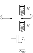 | 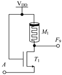 |
| MOS Transistor Threshold Voltage | VDD < vth1 ≤ 2VDD | VDD < vth1 ≤ 2VDD | VDD <vth1 ≤ 2VDD |
| Logic Function | F10, F13 | F18 | F23, F26 |
| Circuit Structure |  | 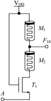 | 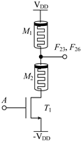 |
| MOS Transistor Threshold Voltage | F10: 0V < vth1 ≤ VDD F13: VDD <vth1 ≤ 2VDD | VDD <vth1 ≤ 2VDD | F23: 0V < vth1 ≤ VDD F26: VDD <vth1 ≤ 2VDD |
| Logic Function | F2 | F3 | F7 | F11 | F15 | F17 | F21 | F24 |
| Composition | F26 + F4 | F25 + F19 | F4 + F9 | F4 + F10 | F25 + F26 | F4 + F18 | F4 + F19 | F4 + F23 |
| Logic Function | Up-Spin Logic Function, F16 | Down-Spin Logic Function, F20 |
|---|---|---|
| Circuit Structure | 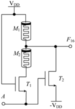 | 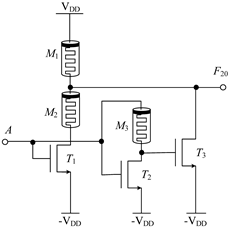 |
| MOS Transistor Threshold Voltage | T1:vth1 > VDD T2:vth2 ≤ 2VDD | T1:vth1 > VDD T2:vth2 ≤ 2 VDD T3:0V < vth3 ≤ VDD |
| Logic Function | F8 | F12 |
| Composition | F20 + F22 | F16 + F22 |
| Input | Output | ||||
|---|---|---|---|---|---|
| Half Adder | Multiplier | Numeric Comparator | |||
| A | B | SUM | CARRY | MUL | MLE |
| −1 | −1 | 1 | −1 | 1 | 0 |
| −1 | 0 | −1 | 0 | 0 | −1 |
| −1 | 1 | 0 | 0 | −1 | −1 |
| 0 | −1 | −1 | 0 | 0 | 1 |
| 0 | 0 | 0 | 0 | 0 | 0 |
| 0 | 1 | 1 | 0 | 0 | −1 |
| 1 | −1 | 0 | 0 | −1 | 1 |
| 1 | 0 | 1 | 0 | 0 | 1 |
| 1 | 1 | −1 | 1 | 1 | 0 |
| Half Adder | Multiplier | Numeric Comparator |
|---|---|---|
 |  |  |
| Method | Components | ||
|---|---|---|---|
| THA | MUL | MLE | |
| Method in This Paper | 46 (13T33M) | 23 (7T16M) | 29 (9T20M) |
| Multiplexer-Based Method in [31] | 74 (10T64M) | 38 (10T28M) | 56 (10T46M) |
| Method | Avg. Power (uW) | Static Power (uW) | Dynamic Power (mW) | ||||||
|---|---|---|---|---|---|---|---|---|---|
| THA | MUL | MLE | THA | MUL | MLE | THA | MUL | MLE | |
| Method in this paper | 246.99 | 72.84 | 0.31 | 698 [−1&1] | 193 [−1&1] | 1.88 [0&−1] | 3.61 | 4.56 | 1.44 |
| Method in [27] | 72.65 | 72.84 | 0.56 | 201 [−1&1] | 181 [0&1] | 1.51 [0&−1] | 5.06 | 4.59 | 1.63 |
Disclaimer/Publisher’s Note: The statements, opinions and data contained in all publications are solely those of the individual author(s) and contributor(s) and not of MDPI and/or the editor(s). MDPI and/or the editor(s) disclaim responsibility for any injury to people or property resulting from any ideas, methods, instructions or products referred to in the content. |
© 2023 by the authors. Licensee MDPI, Basel, Switzerland. This article is an open access article distributed under the terms and conditions of the Creative Commons Attribution (CC BY) license (https://creativecommons.org/licenses/by/4.0/).
Share and Cite
Wang, X.; Zhang, X.; Dong, C.; Nath, S.K.; Iu, H.H.-C. Design and Application of Memristive Balanced Ternary Univariate Logic Circuit. Micromachines 2023, 14, 1895. https://doi.org/10.3390/mi14101895
Wang X, Zhang X, Dong C, Nath SK, Iu HH-C. Design and Application of Memristive Balanced Ternary Univariate Logic Circuit. Micromachines. 2023; 14(10):1895. https://doi.org/10.3390/mi14101895
Chicago/Turabian StyleWang, Xiaoyuan, Xinrui Zhang, Chuantao Dong, Shimul Kanti Nath, and Herbert Ho-Ching Iu. 2023. "Design and Application of Memristive Balanced Ternary Univariate Logic Circuit" Micromachines 14, no. 10: 1895. https://doi.org/10.3390/mi14101895
APA StyleWang, X., Zhang, X., Dong, C., Nath, S. K., & Iu, H. H.-C. (2023). Design and Application of Memristive Balanced Ternary Univariate Logic Circuit. Micromachines, 14(10), 1895. https://doi.org/10.3390/mi14101895