Abstract
Wearable medical devices (WMDs) that continuously monitor health conditions enable people to stay healthy in everyday situations. A wristband is a monitoring format that can measure bioelectric signals. The main part of a wearable device is its analog front end (AFE). Wearables have issues such as low reliability, high power consumption, and large size. A conventional AFE device uses more analog-to-digital converters, amplifiers, and filters for individual electrodes. Our proposed MUX-based AFE design requires fewer components than a conventional AFE device, reducing power consumption and area. It includes a single-ended differential feedback operational transconductance amplifier (OTA) and n-pass MUX-based AFE circuits which are related to the emergence of low power, low area, and low cost AFE-integrated chips that are required for wearable biomedical applications. The proposed 6T n-pass multiplexer measures a gain of −68 dB across a frequency range of 100 kHz with a 136.5 nW power consumption and a delay of 0.07 ns. The design layout area is approximately 9.8 µm2 and uses 45 nm complementary metal oxide semiconductor (CMOS) technology. Additionally, the proposed single-ended differential OTA has an obtained input referred noise of 0.014 µVrms, and a gain of −5.5 dB, while the design layout area is about 2 µm2 and was designed with the help of the Cadence Virtuoso layout design tool.
1. Introduction
The healthcare systems of all nations must adapt to the difficulties posed by new diseases, as well as dietary habits, way of life changes, environmental changes, and other factors. Researchers face novel and fascinating challenges due to the consumer healthcare market’s requirements, which are influenced by statistically solid characteristics of human populations (such as age or income) [1,2]. A World Health Organization (WHO) report reports that the leading cause of death globally are cardiovascular diseases (CVDs), which are expected to claim 17.90 million lives annually [3].
The Stroke and Heart Disease Statistics Update Fact Sheet provides information about the global prevalence of heart disease, stroke, and other ailments [4]. Strokes and heart attacks account for around 32 of every 100 deaths from CVD worldwide. In 2030, 1.56 billion people will have high blood pressure (BP), sometimes known as hypertension. Early detection and management of medical problems can significantly impact healthcare costs and survival rates. Medical professionals can now identify ailments earlier than ever due to biomedical technologies. They can now offer more individualized care and lower the possibility of difficulties during perfusion. It is possible to identify risks and treat medical diseases more quickly and effectively using wearables [5,6,7,8].
Rapid progress in the field of miniaturization within the electronic industry has made it possible to create more adaptive, reliable, and wearable devices. This might cause a global change in health systems toward the continuous monitoring of body health conditions [9]. Biomedical devices can be categorized as wearable and implantable therapeutic devices [10]. A WMD is a self-contained, non-invasive object that carries out a specific therapeutic or diagnostic purpose [11]. More research on WMDs was conducted between 2003 and 2023, and our literature analysis shows that this sector is proliferating. The use of wearable medical technology has vastly improved over the past decade, especially in the remote monitoring of people [12].
A WMD is a risk-detection device that must be small, light, and comfortable [13]. The three major industry sectors for the wearable market have been projected to be consumer electronics, defense, and health care. Smartwatches and bands are the most popular wearables on the market, according to statistics from the [14] Vandrico wearable index. This survey shows that 54% of wearables are functional, fashionable, wrist-mounted devices that consume a minimal amount of power among.
An essential part of a WMD is shown in Figure 1. This wrist-worn device measures all biological signals with a 2 mW power consumption and a 1.2 V power supply [15]. With the help of wearable sensors, abnormal signals can be detected quickly, and medical aid can be provided promptly [16]. The constant electrode or sensor placement dramatically depends on the area where the biological signal is gathered from the skin surface [17]. An AFE primarily consists of amplifiers, filters, and analog-to-digital converter (ADC) blocks. Input voltages from electrode sensors are detected, amplified, filtered, and pre-processed by the amplifier and filter blocks. The output voltage is then converted into a digital signal by an ADC, which then transmits the signal to a transmitter [18]. A smartphone or comparable device receives the transmitted signal for real-time viewing. The data will then be sent to the cloud for additional processing and reporting to nearby physicians.
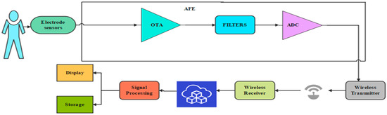
Figure 1.
General block diagram of WMD.
The following discussion will be focused on previous research that was published regarding each block and how their designs were put into implementation. A 0.18 µW CMOS fabrication method was used to create an AFE—CMOS circuit proposed by Zhu et al. While occupying 1 mm2, it only consumes 1.3 µW at 0.5 V [19]. Kong [20] has proposed a pseudo-differential capacitive MEMS accelerometer AFE design using 0.18 µm CMOS technology. Output modulation moves the low-frequency capacitance sensor output from 2 to 12 kHz to the high frequency 800 kHz range. In turn, it receives a CMRR of 95 dB and a 0.5–250 Hz span. The main part of our proposed WMD is an MUX-based AFE design with a 4 × 1 6 T n-pass multiplexer, a single-ended differential feedback OTA, and a low-power CMOS Schmitt trigger. Simulations undertaken with the Cadence Virtuoso tool show that the proposed AFE design, which uses 45 nm technology with a span of 100 kHz, uses less power and takes up less space in an integrated IC design.
Previous research has shown that a healthy resting heart rate should range between 50 and 70 beats per minute [21]. Electrocardiography (ECG) electrodes convert beats into voltage, which then produce extremely weak signals ranging from 0.5 mV to 5.0 mV [22]. A normal electromyography (EMG) signal typically has an amplitude of 10 mV and a bandwidth of 0–500 Hz, with the dominant frequency range being 50–150 Hz [23]. Hypothermia is a drop in body temperature below 95°F. Precision temperature-to-voltage converters, or TC107/TC1047A sensors, can precisely measure temperatures between −40 °C and +125 °C [24]. According to the microchip technology datasheet, the output range is 100 mV at −40 °C, 500 mV at 0 °C, and 750 mV at +25 °C. Nakata et al. [25] have proposed a wearable, flexible, multipurpose healthcare device incorporating an ISFET chemical sensor for simultaneous sweat PH and skin temperature monitoring. Nyein et al. [26] have proposed that a given biological fluid may have a pH level of 3–8, with potentials ranging from 285.6 to 309.8 mV and sensitivities able to determine concentration changes ranging from 60.0 to 65.4 mV/decade.
Dua et al. [27] have designed a 45 nm CMOS MUX for high-speed applications with a supply of 1 to 3 volts, a frequency of 1 MHz, and a power consumption of 92.22 to 146.7 pW. Sharma and Akashe [28] designed multiplexers using XOR-based transmission gate techniques for low-power circuit applications. They compared their designs with different supply voltages from 0.8 to 5 volts and inferred that the power consumption varied from 0.152 µW to 0.829 mW. Kumar et al. [29] have proposed an nMOS 4X1 MUX using dynamic threshold MOS (DTMOS) technology with a 1 V supply and a 42.7 µW power consumption for low-power wearable device applications.
Diab et al. [30] have developed a 130 nm CMOS AFE with adjustable low-pass and high-pass corner frequencies and a mid-band gain of 31 to 52 dB. This is used in low-noise biomedical applications. Then, Singh et al. [31] suggested an OTA-based readout front-end with a power consumption of 145.9 nW and a CMRR of 71.39 dB as an alternative to the current-mode method. This study defines a fundamental and unique structure while considering electrical characteristics such as DC gain and linearity. Later, Gifta et al. [32] proposed an ultra-low-power bulk-driven OTA circuit for biological applications. In this circuit, the double recycling technique was applied with a 0.4 V supply voltage, which increased the DC gain and slew rate.
The Schmitt trigger, a 1-bit digitizer with pulse hysteresis, is one of the most vital parts of the ADC because it digitalizes the amplified biological signal. Parveen et al. [33] have claimed that current sink and current source inverters be used to build Schmitt trigger circuits for low-power and high-speed applications. The main advantage of the recommended circuits, which make use of a 180 nm CMOS model with cadence and a supply rail voltage of +3 V, is that they have stable output amplitudes in the 0° to 100 °C range. Pahlavan et al. [34] have suggested a dual-band Schmitt trigger suitable for multiband and high-performance applications. The power consumption and delay of the proposed delay element are 103–581 ps and 4.23–1.04 mW for CMOS 180 nm standard technology, respectively.
The proposed WMD architecture has been designed by sharing amplifiers and filters across a large number of electrodes using the rapid multiplexing technique, as shown in Figure 2.
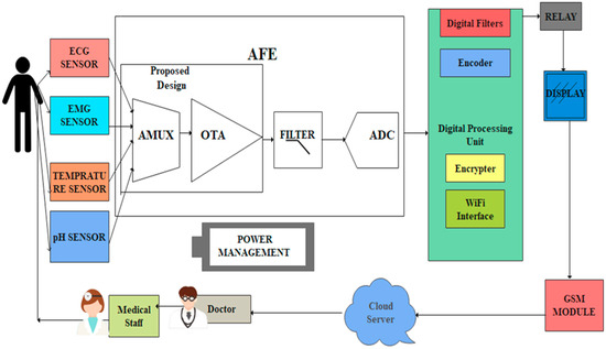
Figure 2.
The proposed architecture of WMD with AFE.
Biophysical symptoms, including pain, fatigue, and heart problems, can all be better diagnosed with the use of EMG, ECG, pH, and temperature readings. The simultaneous collection of multiple signals simplifies the identification of the root cause of stress- or discomfort-related illnesses. The AFE includes a 4 × 1 MUX that receives bio-information from EMG, ECG, pH values, and temperature sensors. AFE is essential in WMDs for signal amplification and for identifying human abnormalities.
Each electrode in a conventional AFE must have its own amplifier, filter, and ADC converter, which creates a variety of design challenges, such as the large active area of resistors, complexity, scalability, and power consumption [35,36,37]. The MUX-based AFE is suggested in this study as a solution to these problems. An analog 6T n-pass time division multiplexer, a single-ended fully differential OTA, and a low-power Schmitt trigger have all been designed for the proposed MUX-based AFE. The performance of each component has been evaluated using CMOS technologies.
Individuals are monitored via a wearable device, which must be worn at all times. This detects deviations from the typical pre-set values and alerts the end user so they can take the right action. A crew and medical professionals regularly observe the patients using the Internet of Things (IoT) in their current circumstances. The solution might be a continuous monitoring system that guards against casualties while urging the crew to seek medical attention in emergencies.
2. Materials and Methods
2.1. Design a 4 × 1 Multiplexer Using n-Pass Time Division Techniques
The proposed 4 × 1 n-pass time division analog multiplexer design is depicted in Figure 3a using 45 nm CMOS technology. The 4 × 1 time division multiplexing (TDM) technique sends four distinct signals across a signal line using synchronized switches, which are transmitted sequentially in time. The multiplexer has been designed using low-power pass transistor logic (LPPTL), which requires only six transistors. The source/drain terminals of the n-pass transistors are connected to the inputs from electrodes with dimensions of L = 45 nm and W = 120 nm. Figure 3b illustrates the physical layout structure of a 4 × 1 n-pass MUX.
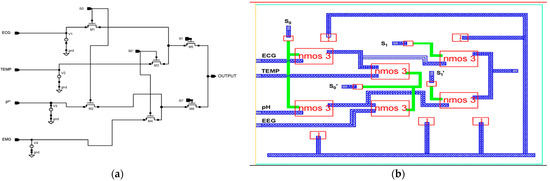
Figure 3.
Proposed 45 nm low power n-pass 4 × 1 MUX. (a) Schematic diagram and (b) layout structure.
The sampled input values are taken from the sensors: 10 mV for EMG, 63.3 mV for pH, 100 mV for temperature, and 5.0 mV for ECG. The truth table for the 4 × 1 n-pass time division analog multiplexer used in the circuit diagram is presented in Table 1. The selection lines S1, and S0 select which inputs should be relayed to the output. Every input has a potential generated by Equation (1) [38].
Output = S1′S0′ EMG + S1′S0 TEMP + S1S0′ pH Value + S1S0 ECG.

Table 1.
Proposed 4 × 1 MUX truth table.
The pass transistor logic reduces the number of transistors needed to implement logic by allowing the primary inputs drive both the gate and source-drain terminals. It operates 88% faster, reduces area by 70%, and consumes 81.9% less energy than fully complementary MOS logic.
2.2. Design of Low Power Differential Feedback OTA
In this section, a single-stage differential positive feedback OTA has been designed using source degeneration techniques, as shown in Figure 4a. When significant signals are applied, the circuit converts a differential pair input voltage into the current as an output. The bias circuit generates an external voltage that serves as a reference voltage and drives the entire circuitry. We have drawn the physical layout structure, depicted in Figure 4b, with dimensions of 14.4 μm × 14.45 μm.
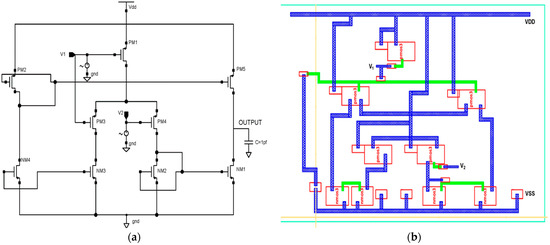
Figure 4.
Proposed 45 nm low power differential feedback OTA design. (a) Schematic diagram and (b) layout structure.
PMOS transistors are used in the input stage because of their low flicker noise output. The transistors PM1–PM4 make up the differential gain stage, the input’s first stage. The gate terminals of the transistors PM1 and PM2 are correspondingly connected with the differential voltage signal. This OTA is built with two voltages, Vin+ and Vin-, coupled to NM2 and NM3, respectively. Transistors PM1 and PM2 are coupled back-to-back in the first stage. The gates of each CMOS transistor are electrically connected with this technology.
The differential amplifier characteristics of transistors PM3 and NM4 allow for reduced power usage. While NMOS transistors, such as NM1, NM2, and NM4 operate in the sub-threshold zone and need less power, PMOS transistors such as PM1, PM2, and PM3 operate in the linear area.
Total charge
where current I = Q/τ, τ is transient time.
Q = WL C ox [(V GS − V T H) − 0.5 V DS].
The current equation for CMOS is
ID = µCoxW/L [(VGS − V T H) VDS − V2DS/2]
The total charge Q is expressed in Equation (2) [39], where W/L represents the transistors’ width-to-length ratios, ID is the drain current, µ is the MOS transistor’s mobility, Cox is the oxide layer’s capacitance, VGS is the gate-to-source voltage, VTH is the threshold voltage, and VDS is the drain-to-source voltage. To create a linear transconductor with a broad input operating range, the proposed design is subject to a four-NMOS transistor cell that gives a low transconductance path. In the design of the fully differential transconductor, two output currents, I1 and I2, are produced by the voltage-to-current converter (V–I). The output current Io is linearly proportional to the differential input voltage (Vol1 − Vol2), such that Io = I2 − I1 = G (Vol1 − Vol2), where G is the equivalent transconductance. Equation (3) [39] is used to design a low-power differential feedback OTA architecture and analyze the drain current (ID) using a 45 nm CMOS model with minimum transistor sizing. The NMOS and PMOS transistor sizing are given in Table 2 and Table 3.
Table 2.
PMOS sizing.
Table 3.
NMOS sizing.
A low-power differential feedback OTA design is developed using Equations (4) and (5) [36], and the drain current ID is evaluated using a 45 nm CMOS mode. The configurations of PMOS and NMOS are then sized in terms of length, width, finger, threshold, and SD metal width based on Table 2 and Table 3, mentioned above. It is possible to find the perfect transistor size for a given set of requirements by using optimization techniques. Transistor sizing is often required for a number of performances, including the transconductance parameter of the NMOS, PMOS (kn, kp) Equations (3) and (5), and the transconductance of the NMOS, PMOS (gmn, gmp) Equations (6) and (7) [40]. This is used to analyze the OTA’s power consumption, gain, frequency response, and linearity [41].
For NMOS, the transconductance parameter factor (kn) is:
kn = µnCox(W/L); Vtn > 0; VDS ≥ 0; Vov = VGS − Vtn
Transconductance of NMOS (gmn) is
gmn = knVov
With PMOS, the formula for the PMOS transconductance parameter factor (kp) is:
kp = µpCox(W/L); Vtp < 0; VSD ≥ 0; Vov = VSG − |Vtp|
The PMOS transconductance (gmp) is given by
where µn is the mobility of the NMOS transistor, µp is the mobility of the PMOS transistor, Cox is the capacitance of the oxide layer, VGS is the gate-to-source voltage, W/L is the width-to-length ratio of the transistors, Vtn is the threshold voltage of the NMOS transistor, Vtp is the threshold voltage of the PMOS transistor, and VDS is the voltage from the drain to the source. Vov is a voltage for overdrive.
gmp = kp.Vov
The transistors NM1–NM4 make up the differential gain stage, which is the input’s first stage. The gate terminals of the transistors PM1 and PM4 are correspondingly connected with the differential voltage signal. PM2, PM3, and PM5 give a balanced differential gain to the entire circuit with a high driving capacitive. The proposed OTA is a voltage-controlled current source, which provides the benefit of a significantly lower transistor count. This is the most straightforward and successful OTA for wearable medical applications.
2.3. Design of Low-Power CMOS Schmitt Trigger
Figure 5 depicts a CMOS Schmitt trigger that digitizes an analog input signal at a low-level supply voltage. Self-bias transistors PM0, NM7, NM2, and PM5 lower the effective supply voltage level. The transistors PM3 and NM3’s width and length can be changed to create pulse hysteresis. When the input voltage is low, NM1 is disabled and PM1, PM2, and NM0 currents are almost zero. The output begins to decline as soon as NM0 is turned on.
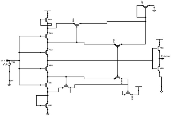
Figure 5.
Schematic diagram of 45 nm proposed CMOS Schmitt trigger.
Before NM0 is turned on, the currents of NM4 and NM1 are equal. We considered the use of a low-power CMOS Schmitt trigger and a low-level supply voltage was used to digitize the input-modulated signal in this device. Transistors that self-bias were utilized to lower the supply voltage’s level. A voltage inverter was utilized at the output to balance the voltage swing. The circuit was simulated using 45 nm CMOS technology at a 100 Hz input sine wave. According to the simulation results, the suggested Schmitt trigger used a 0.8 V supply and a standard 45 nm PMOS and NMOS size to consume 1.22 nW power.
2.4. Design of AFE IC
This patient-monitoring IC is an AFE for recording numerous vital human body parameters through the skin. This AFE-on-a-chip enables clinical-grade vital sign measurement and bio-signal processing for patient health assessment, focusing on manufacturers of compact, battery-operated, constantly wearable devices.
Figure 6 illustrates the proposed AFE for WMD applications, which consists of the 4 × 1 time division multiplexer, differential OTA, and low-power Schmitt trigger. Vital human body signals, i.e., ECG, EMG, pH values, and temperature, are combined by the 4 × 1 time division multiplexer, which also uses a low-power Schmitt-trigger ADC to digitize current signals from OTA. In total, the proposed AFE consists of 29 transistors and consumes 2.62 pW power from a 0.8 V supply voltage. Cadence Virtuoso tools, styled as cādence, is an American international computational software firm headquartered in San Jose, California. It was created in 1988 through the merging of SDA Systems and ECAD, Inc. These tools offer a robust design environment and were utilised in the present research for analysis purposes. The Cadence Licence Manager was successfully installed and executed on a Linux-based personal computer operating on the Ubuntu distribution.
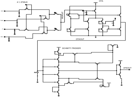
Figure 6.
Schematic diagram of the 45 nm proposed AFE design for WMD.
3. Results and Discussion
3.1. Proposed 4 × 1 Multiplexer Simulation Results and Comparison Analysis
3.1.1. Transient Response
In our proposed design, the output produced the least possible delay due to time division multiplexing techniques. The combination of inputs at the selection lines S0 and S1 determines the multiplexer’s output. The sensors’ sampled input values were 10 mV for EMG, 63.3 mV for pH, 100 mV for temperature, and 5.0 mV for ECG. The 4 × 1 MUX transient response output wave form is seen in Figure 7. Marker M1 indicates an 11.21083 ns output as 100.0002 mV, which is the temperature output when the pulse input S0 = 1, S1 = 0 with the least error 0.0002, indicating our proposed circuit runs more accurately.
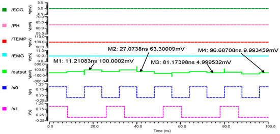
Figure 7.
The 4 × 1 MUX transient response output wave form.
3.1.2. AC Analysis
The 180 nm 4 × 1 multiplexer’s phase-versus-gain output curve, shown in Figure 8a, indicates that the cutoff frequency is 586.1 kHz and the gain is −204.9 mdB, with a 3 dB phase margin of −16.68°. Figure 8b shows the 90 nm 4 × 1 multiplexer output curve, with a cutoff frequency of 203.652 kHz, a gain of −133.92 mdB, and a 3 dB phase margin of −31.76°. The 45 nm 4 × 1 multiplexer’s phase-versus-gain output curve is shown in Figure 8c. The above results show that the gain margin (GM) increases the stability of the 4 × 1, which is suitable for accurately gathering and analyzing the bio-signal from the sensors.
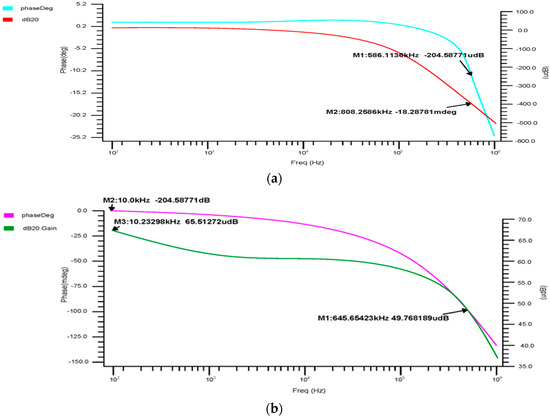
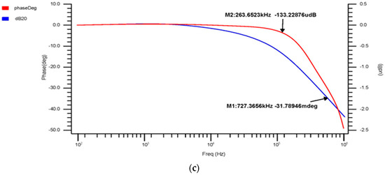
Figure 8.
4 × 1 MUX phase-versus-gain AC response for the (a) 180 nm technology, (b) 90 nm technology and (c) 45 nm technology.
3.1.3. Comparison Results of 4 × 1 MUX
This research analyzed in detail the low-power 4x1-MUX n-MOS 6T pass transistor logic. Table 4 demonstrates that 45 nm CMOS-based 6T-n-pass logic requires less power and physical space than other technologies. Table 5 provides the parameter analysis based on simulations undertaken with Cadence Virtuoso, such as area, bandwidth, phase, and gain margin, for 180, 90, and 45 nm technologies. However, the number of transistors in our suggested design is decreased to 6 due to the low-power n-pass- MOS logic technique. Using 45 nm CMOS, a latency of almost 0.07 ns and low power consumption of 136.5 nW have been achieved.
Table 4.
Comparison analysis of 4 × 1 MUX using different technologies from previous research.
Table 5.
Parameter analysis of various CMOS technologies.
3.2. Proposed OTA Simulation Results and Comparison Analysis
3.2.1. Transient Analysis
We have undertaken transient analysis for differential feedback OTA, using 180 nm, 90 nm, and 45 nm technologies as shown in Figure 9a–c, respectively. These consumed 130 nW for the 180 nm, 1.5 nW for the 90 nm, and 1.43 nW for the 45 nm technology. A two-stage operational transconductance amplifier based on 45 nm CMOS technology has been designed and analyzed with a supply voltage of 0.8 V. We inferred that lowering the nm technology produced a low power consumption.
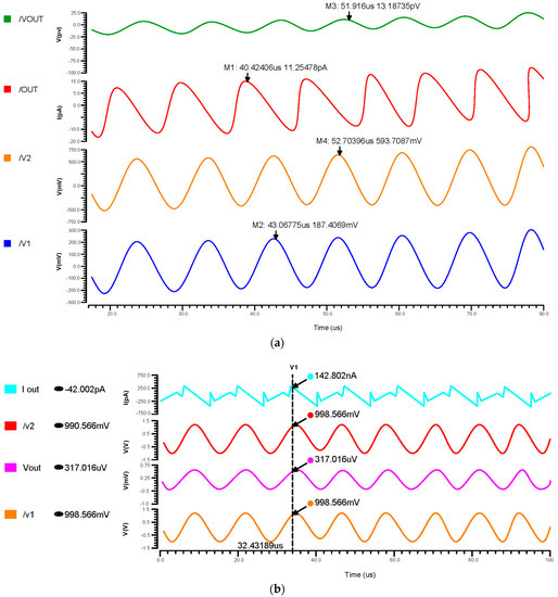
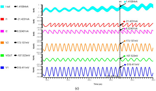
Figure 9.
Transient response of differential OTA using (a) 180 nm technology, (b) 90 nm technology and (c) 45 nm technology.
3.2.2. AC Analysis
The phase and transient reaction are also important components of an amplifier, as the AC frequency response is used to determine the gain and bandwidth. The gain-versus-phase response was analyzed and the gain value was −59.07 dB at 43.19 kHz for 180 nm, 2.97 mdB at 3.75 kHz for 90 nm, and −1.23 dB at 90.40 kHz for 45 nm, as shown in Figure 10a–c.
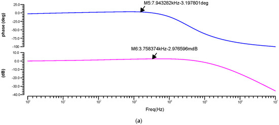
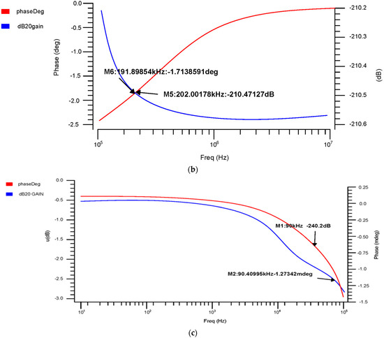
Figure 10.
Differential OTA phase-versus-gain AC response for the (a) 180 nm technology, (b) 90 nm technology and (c) 45 nm technology.
3.2.3. Noise Analysis of Proposed OTA
Each component’s noise contribution is estimated at the output node over the chosen frequency range. The input referred noise has been calculated as 2.05 µmVrms for 180 nm, 0.093 µmVrms for 90 nm, and 14.76 µmVrms for 45 nm, as shown in Figure 11. From these results, the 45 nm technology offered a low noise that brings a noise-free signal amplification for biological applications.
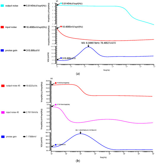
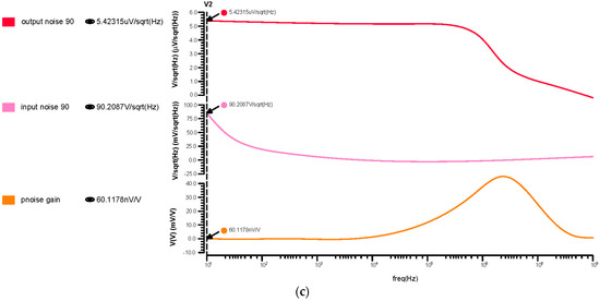
Figure 11.
Differential OTA input, output, and transfer noise response for the (a) 180 nm technology, (b) 90 nm technology and (c) 45 nm technology.
3.2.4. Comparison Results of OTA
From Table 6, we inferred that the proposed design had a low power consumption of 1.43 nW in the 45 nm CMOS technology. Comparing our work historic values revealed that it reached up to 0.014 µVrms and that the noise efficiency factor is 1.6.
Table 6.
Comparison of OTA power with different technology.
3.3. Proposed AFE Simulation Results and Comparison Analysis
Figure 12a indicates that the inputs from the sensors range in voltage from 5 mV to 100 mV, which differential OTA amplifies to about 680 mV, and that their currents are then in the range of about 300 µA, Figure 12b shows that the input of the Schmitt trigger analog current signal is converted to a voltage pulse signal. The Schmitt trigger output ranges from 5 mV to 110 mV, depending on the inputs at different times. Using a differential OTA circuit, an AFE device is able to read analog data from sensors for the ECG, EMG, pH value, and temperature before converting them to current. A Schmitt trigger circuit then changes the current input to pulses by time variation. This is illustrated in Figure 12c.
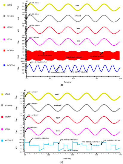
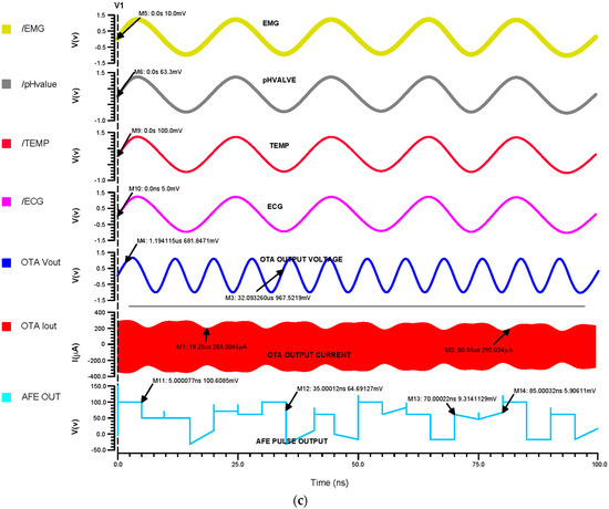
Figure 12.
The (a) 45 nm OTA transient analysis, (b) 45 nm Schmitt trigger transient analysis and (c) 45 nm AFE transient analysis.
As inferred from Table 7, the proposed AFE design demonstrated a low power consumption of 2.62 pW for the 45 nm CMOS technology. The individual power supplies for the MUX, OTA, and Schmitt trigger circuits are consolidated into a single source for all of the different circuits in order to drastically minimize the power needed for the integrated AFE circuit.
Table 7.
AFE power comparison using various technologies.
4. Conclusions
This research shows the design and development of a multiplexer-based AFE for WMD using CMOS techniques. The main part of the proposed WMD is an MUX-based AFE design made up of a 4 × 1 6T n-pass multiplexer, a single-ended differential feedback OTA, and a low-power CMOS Schmitt trigger. According to the results of simulations performed using the Cadence Virtuoso tool, the proposed AFE design, which uses 45 nm technology, only consumes 2.62 pW and occupies less space in an integrated IC design. In addition, the simulation result of the 6T n-pass multiplexer has a gain of −68 dB across a frequency range of 100 kHz and consumes 136.5 nW of power. This is used to combine all of the biosignals, including ECG, EMG, pH, and temperature, for the proposed AFE. The OTA plays a vital role in the AFE device. The suggested circuit for the single-ended differential OTA exhibits a power consumption of 1.43 nW, a gain of −5.5 dB, and a noise factor of 1.6. This circuit enhances the amplification of biosignals, and thus surpasses the previous research in terms of its scope and results. Wearable continuous person monitoring systems may benefit from the usage of MUX-based AFE in our research, which will be used to declare long-lasting battery lifespan for consumer electronics products with reliable, compact real-time monitoring features.
Author Contributions
E.T. contributed a pivotal role in formulating the theoretical framework behind the proposed research, in addition to conducting the necessary computations. G.N.R.D. had responsibility for assessing the analytical methodologies and providing supervision for the outcomes of the project. Each author approves of funding that is equally distributed and endorsed by all authors. The authors participated in a thorough discussion of the findings, ensuring that all perspectives were taken into account and incorporated into the final version of the publication. All authors have read and agreed to the published version of the manuscript.
Funding
This research received no external funding.
Data Availability Statement
The article contains all the necessary data to support the results, and there is no need for any more source data.
Acknowledgments
This research was funded by the Quality Improvement Program and the All India Council for Technical Education Fellowship Scheme for full-time Ph.D. students. The Teachers Associateship for Research Excellence is an opportunity offered by the Science and Engineering Research Board.
Conflicts of Interest
The authors declare no conflict of interest.
References
- Ma, X.; Guo, G.; Wu, X.; Wu, Q.; Liu, F.; Zhang, H.; Shi, N.; Guan, Y. Advances in Integration, Wearable Applications, and Artificial Intelligence of Biomedical Microfluidics Systems. Micromachines 2023, 14, 972. [Google Scholar] [CrossRef] [PubMed]
- Horestani, F.K.; de la Rosa, J.M. Ultra-High-Resistance Pseudo-Resistors with Small Variations in a Wide Symmetrical Input Voltage Swing. IEEE Trans. Circuits Syst. II Express Briefs 2023, 70, 2794–2798. [Google Scholar] [CrossRef]
- Price, A.E. Heart disease and work. Heart 2004, 90, 1077–1084. [Google Scholar] [CrossRef] [PubMed]
- Virani, S.S.; Alonso, A.; Aparicio, H.J.; Benjamin, E.J.; Bittencourt, M.S.; Callaway, C.W.; Carson, A.P.; Chamberlain, A.M.; Cheng, S.; Delling, F.N.; et al. Heart disease and stroke statistics-2021 update: A report from the American Heart Association. Circulation 2021, 143, CIR0000000000000950. [Google Scholar] [CrossRef] [PubMed]
- Saravanan, V.; Priya, R.A.; Venkatalakshmi, B. Design of optimal amplifier for wearable devices. In Proceedings of the 2011 International Conference on Process Automation, Control and Computing, Coimbatore, India, 20–22 July 2011; pp. 1–4. [Google Scholar] [CrossRef]
- Wan, Q.; Wan, C.; Wu, H.; Yang, Y.; Huang, X.; Zhou, P.; Chen, L.; Wang, T.Y.; Li, Y.; Xue, K.H.; et al. 2022 roadmap on neurmorphic devices and applications research in China. Neuromorphic Comput. Eng. 2022, 2, 042501. [Google Scholar] [CrossRef]
- Wang, Y.; Miao, F.; An, Q.; Liu, Z.; Chen, C.; Li, Y. Wearable multimodal vital sign monitoring sensor with fully integrated analog front end. IEEE Sens. J. 2022, 22, 13462–13471. [Google Scholar] [CrossRef]
- Sonkusale, S.; Baghini, M.S.; Aeron, S. Flexible Bioelectronics with Power Autonomous Sensing and Data Analytics; Springer: Berlin/Heidelberg, Germany, 2022; Available online: https://link.springer.com/book/10.1007/978-3-030-98538-7 (accessed on 6 January 2022).
- Inamori, G.; Kamoto, U.; Nakamura, F.; Isoda, Y.; Uozumi, A.; Matsuda, R.; Shimamura, M.; Okubo, Y.; Ito, S.; Ota, H. Neonatal wearable device for colorimetry-based real-time detection of jaundice with simultaneous sensing of vitals. Sci. Adv. 2021, 7, eabe3793. [Google Scholar] [CrossRef]
- Gifta, G.; Gracia Nirmala Rani, D.; Farhana, N.; Archana, R. Design of CMOS based biosensor for implantable medical devices. In Proceedings of the VLSI Design and Test: 22nd International Symposium, VDAT 2018, Madurai, India, 28–30 June 2018; Revised Selected Papers 22. Springer: Singapore, 2019; pp. 695–704. [Google Scholar] [CrossRef]
- Xue, D.; Cai, R.; Liu, Y. Design of amplifier for wearable human ECG sensor with low power and low noise. J. Phys. Conf. Ser. 2021, 1907, 012058. [Google Scholar] [CrossRef]
- Gao, W.; Ota, H.; Kiriya, D.; Takei, K.; Javey, A. Flexible electronics toward wearable sensing. Acc. Chem. Res. 2019, 52, 523–533. [Google Scholar] [CrossRef]
- Sylvester, D.; Srivastava, A. Computer-aided design for low-power robust computing in nanoscale CMOS. Proc. IEEE 2007, 95, 507–529. [Google Scholar] [CrossRef]
- Vandrico. Wearable Technology Database. Available online: https://vandrico.com/wearables/ (accessed on 6 January 2022).
- Kim, I.; Bhagat, Y.A.; Homer, J.; Lobo, R. Multimodal analog front end for wearable bio-sensors. IEEE Sens. J. 2016, 16, 8784–8791. [Google Scholar] [CrossRef]
- Sharma, M. Electrode Multiplexed CMOS Front-End for Extracellular Neural Recording. Ph.D. Thesis, The University of Utah, Salt Lake, UT, USA, 2020. [Google Scholar]
- Athavale, Y.; Krishnan, S. Biosignal monitoring using wearables: Observations and opportunities. Biomed. Signal Process. Control 2017, 38, 22–33. [Google Scholar] [CrossRef]
- Lee, J.; Song, S.; Roh, J. A 103 dB DR Fourth-Order Delta-Sigma Modulator for Sensor Applications. Electronics 2019, 8, 1093. [Google Scholar] [CrossRef]
- Zhu, Z.; Bai, W. A 0.5-V 1.3-µW Analog Front-End CMOS Circuit. IEEE Trans. Circuits Syst. II Express Briefs 2016, 63, 523–527. [Google Scholar] [CrossRef]
- Kong, D.; Duan, Q.A. Pseudo-Differential Capacitive MEMS Accelerometer Analog Front-End Design. J. Phys. Conf. Ser. 2023, 2477, 012033. [Google Scholar] [CrossRef]
- Kamilya, T.; Park, J. Highly Sensitive Self-Powered Biomedical Applications Using Triboelectric Nanogenerator. Micromachines 2022, 13, 2065. [Google Scholar] [CrossRef]
- Yang, Y. Design of Low-Power Low-noise CMOS ECG Amplifier for Smart Wearable Device. J. Phys. Conf. Ser. 2020, 1642, 012027. [Google Scholar] [CrossRef]
- Li, Y.; Poon, C.C.; Zhang, Y.T. Analog integrated circuits are designed for processing physiological signals. IEEE Rev. Biomed. Eng. 2010, 3, 93–105. [Google Scholar] [CrossRef]
- Lopez, X.; Afrin, K.; Nepal, B. Examining the design, manufacturing, and analytics of smart wearables. Med. Devices Sens. 2020, 3, e10087. [Google Scholar] [CrossRef]
- Nakata, S.; Arie, T.; Akita, S.; Takei, K. Wearable, flexible, and multifunctional healthcare device with an ISFET chemical sensor for simultaneous sweat pH and skin temperature monitoring. ACS Sens. 2017, 2, 443–448. [Google Scholar] [CrossRef]
- Nyein, H.Y.; Gao, W.; Shahpar, Z.; Emaminejad, S.; Challa, S.; Chen, K.; Fahad, H.M.; Tai, L.C.; Ota, H.; Davis, R.W.; et al. A wearable electrochemical platform for noninvasive simultaneous monitoring of Ca2+ and pH. ACS Nano 2016, 10, 7216–7224. [Google Scholar] [CrossRef] [PubMed]
- Dua, T.; Rajput, A. 2:1 Multiplexer Using Different Design Styles: Comparative Analysis. STM J. Adv. Robot. 2020, 7, 5–13. [Google Scholar]
- Sharma, V.K.; Akashe, S. Power Efficient Design of 4: 1 Multiplexer using Low Power Techniques. Int. J. Mod. Eng. Manag. Res. 2016, 4, 44–49. [Google Scholar]
- Kumar, A.; Kandari, R.; Bharti, S. Performance analysis of 4:1 multiplexer with DTMOS technique. In Proceedings of the 2019 4th International Conference on Internet of Things: Smart Innovation and Usages (IoT-SIU), Ghaziabad, India, 18–19 April 2019; pp. 1–6. [Google Scholar] [CrossRef]
- Diab, M.S.; Mahmoud, S.A. 14:5nW; 30 dB Analog Front-End in 90-nm Technology for Biopotential Signal Detection. In Proceedings of the 2020 43rd International Conference on Telecommunications and Signal Processing (TSP), Milan, Italy, 7–9 July 2020; pp. 681–684. [Google Scholar] [CrossRef]
- Singh, W.; Deb, S.; Bahubalindruni, P. Low-noise energy efficient readout front-end for wearable continuous blood pressure monitoring systems. IEEE Trans. Consum. Electron. 2020, 66, 318–326. [Google Scholar] [CrossRef]
- Gifta, G.; Rani, D.G.; Nirmal, D. A 1-V, 5 μW, Atto Current Bulk-Driven CMOS Based Operational Transconductance Amplifier for Biosensor Applications. ECS J. Solid State Sci. Technol. 2020, 9, 115003. [Google Scholar] [CrossRef]
- Parveen, S.A.; Rukmini, M.S.; Srinivasulu, A. Two new Schmitt trigger circuits based on the current sink and current source inverters. In Proceedings of the 2015 International Conference on Signal Processing and Communication Engineering Systems, Guntur, India, 2–3 January 2015; pp. 10–14. [Google Scholar] [CrossRef]
- Pahlavan, S.; Ghaznavi-Ghoushchi, M.B. A differential dual delay mode Schmitt Trigger with 449ps delay gap by reconfiguring with one bit and FVF current source. In Proceedings of the 2016 24th Iranian Conference on Electrical Engineering (ICEE), Shiraz, Iran, 10–12 May 2016; pp. 1580–1585. [Google Scholar] [CrossRef]
- Zhong, L.; Liu, S.; Shang, P.; Cao, W.; Zhu, Z. A 100-to-10-kHz 5.4-to-216-µW Power-Efficient Readout Circuit Employing Closed-Loop Dynamic Amplifier for MEMS Capacitive Accelerometer. IEEE J. Solid-State Circuits 2023, 58, 2226–2238. [Google Scholar] [CrossRef]
- Kosari, A.; Breiholz, J.; Liu, N.; Calhoun, B.H.; Wentzloff, D.D. A 0.5 V 68 nW ECG monitoring analog front-end for arrhythmia diagnosis. J. Low Power Electron. Appl. 2018, 8, 27. [Google Scholar] [CrossRef]
- Pantelopoulos, A.; Bourbakis, N. A survey on wearable biosensor systems for health monitoring. In Proceedings of the 2008 30th Annual International Conference of the IEEE Engineering in Medicine and Biology Society, Vancouver, BC, Canada, 20–25 August 2008; pp. 4887–4890. [Google Scholar] [CrossRef]
- Sharma, M.; Pandey, D.; Palta, P.; Pandey, B.K. Design and power dissipation consideration of PFAL CMOS V/S conventional CMOS based 2:1 multiplexer and full adder. Silicon 2022, 14, 4401–4410. [Google Scholar] [CrossRef]
- Sharan, T.; Bhadauria, V. Fully differential operational transconductance amplifier with enhanced phase margin and gain for ultra-low-power circuits. J. Low Power Electron. 2017, 13, 520–535. [Google Scholar] [CrossRef]
- Gifta, G.; Rani, D.G. Power approaches for biosensors based bio-medical devices. ECS J. Solid State Sci. Technol. 2020, 9, 121005. [Google Scholar] [CrossRef]
- Rani, D.G.; Gifta, G.; Meenakshi, M.; Gomathy, C.; Gowsalaya, T. Design and analysis of CMOS low power OTA for biomedical applications. In Proceedings of the 2019 4th International Conference on Recent Trends on Electronics, Information, Communication & Technology (RTEICT), Bangalore, India, 17–18 May 2019; pp. 871–876. [Google Scholar] [CrossRef]
- Jain, P.; Joshi, A.M. Analyzing the impact of augmented transistor NMOS configuration on parameters of 4x1 multiplexer. Radioelectron. Commun. Syst. 2018, 61, 121–127. [Google Scholar] [CrossRef]
- Nève, A.; Flandre, D.; Quisquater, J.J. SOI technology for future high-performance smart cards. IEEE Micro 2003, 23, 58–67. [Google Scholar] [CrossRef]
- Saputra, N.; Danesh, M.; Baiano, A.; Ishihara, R.; Long, J.R.; Karaki, N.; Inoue, S. An assessment of µ-Czochralski, single-grain silicon thin-film transistor technology for large-area, sensor and 3-D electronic integration. IEEE J. Solid-State Circuits 2008, 43, 1563–1576. [Google Scholar] [CrossRef]
- Zarifi, T.; Peng, C.C.; Zarifi, M.H. Low-power amplifier for in-vivo EEG signal recording. In Proceedings of the 2011 1st Middle East Conference on Biomedical Engineering, Sharjah, United Arab Emirates, 21–24 February 2011; pp. 19–22. [Google Scholar] [CrossRef]
- Joshi, S.; Thaker, V.; Amaravati, A.; Shojaei-Baghini, M. Low-power low-noise analog signal conditioning chip with on-chip drivers for healthcare applications. Microelectron. J. 2012, 43, 828–837. [Google Scholar] [CrossRef]
- Mahmoud, S.A.; Bamakhramah, A.; Al-Tunaiji, S.A. Six order cascaded power line notch filter for ECG detection systems with noise shaping. Circuits Syst. Signal Process. 2014, 33, 2385–2400. [Google Scholar] [CrossRef]
- Yehoshuva, C.; Rakhi, R.; Anto, D.; Kaurati, S. 0.5 V, ultra-low power multi standard G m-C filter for biomedical applications. In Proceedings of the 2016 IEEE International Conference on Recent Trends in Electronics, Information & Communication Technology (RTEICT), Bangalore, India, 20–21 May 2016; pp. 165–169. [Google Scholar] [CrossRef]
- Udupa, S.S.; Sushma, P.S. ECG analog front-end in 180 nm CMOS technology. In Proceedings of the 2017 International Conference on Intelligent Computing, Instrumentation and Control Technologies (ICICICT), Kerala, India, 6–7 July 2017; pp. 327–330. [Google Scholar] [CrossRef]
- Viana, N.L.; Belfort, D.R. A low-power low-noise instrumentation amplifier for wearable applications. In Proceedings of the 2019 4th International Symposium on Instrumentation Systems, Circuits and Transducers (INSCIT), Sao Paulo, Brazil, 26–30 August 2019; pp. 1–5. [Google Scholar] [CrossRef]
- Bano, S.; Narejo, G.B.; Usman Ali Shah, S.M. Low voltage low power single ended operational transconductance amplifier for low frequency applications. Wirel. Pers. Commun. 2019, 106, 1875–1884. [Google Scholar] [CrossRef]
- Zheng, K.; Sun, Y.; Zhang, Y. An ultra-low-power ECG amplifier for wearable devices using classical 2-stage OTA. J. Phys. Conf. Ser. 2021, 1907, 012008. [Google Scholar] [CrossRef]
- Jaikla, W.; Sangyaem, S.; Supavarasuwat, P.; Khateb, F.; Minaei, S.; Kulej, T.; Suwanjan, P. Reconfigurable Voltage-Mode First-Order Multifunction Filter Employing Second-Generation Voltage Conveyor (VCII) with Complete Standard Functions and Electronically Controllable Modification. IEEE Access 2023, 11, 56152–56169. [Google Scholar] [CrossRef]
Disclaimer/Publisher’s Note: The statements, opinions and data contained in all publications are solely those of the individual author(s) and contributor(s) and not of MDPI and/or the editor(s). MDPI and/or the editor(s) disclaim responsibility for any injury to people or property resulting from any ideas, methods, instructions or products referred to in the content. |
© 2023 by the authors. Licensee MDPI, Basel, Switzerland. This article is an open access article distributed under the terms and conditions of the Creative Commons Attribution (CC BY) license (https://creativecommons.org/licenses/by/4.0/).