
Implementation of Flip-Chip Microbump Bonding between InP and SiC Substrates for Millimeter-Wave Applications

 ,
,  and
and 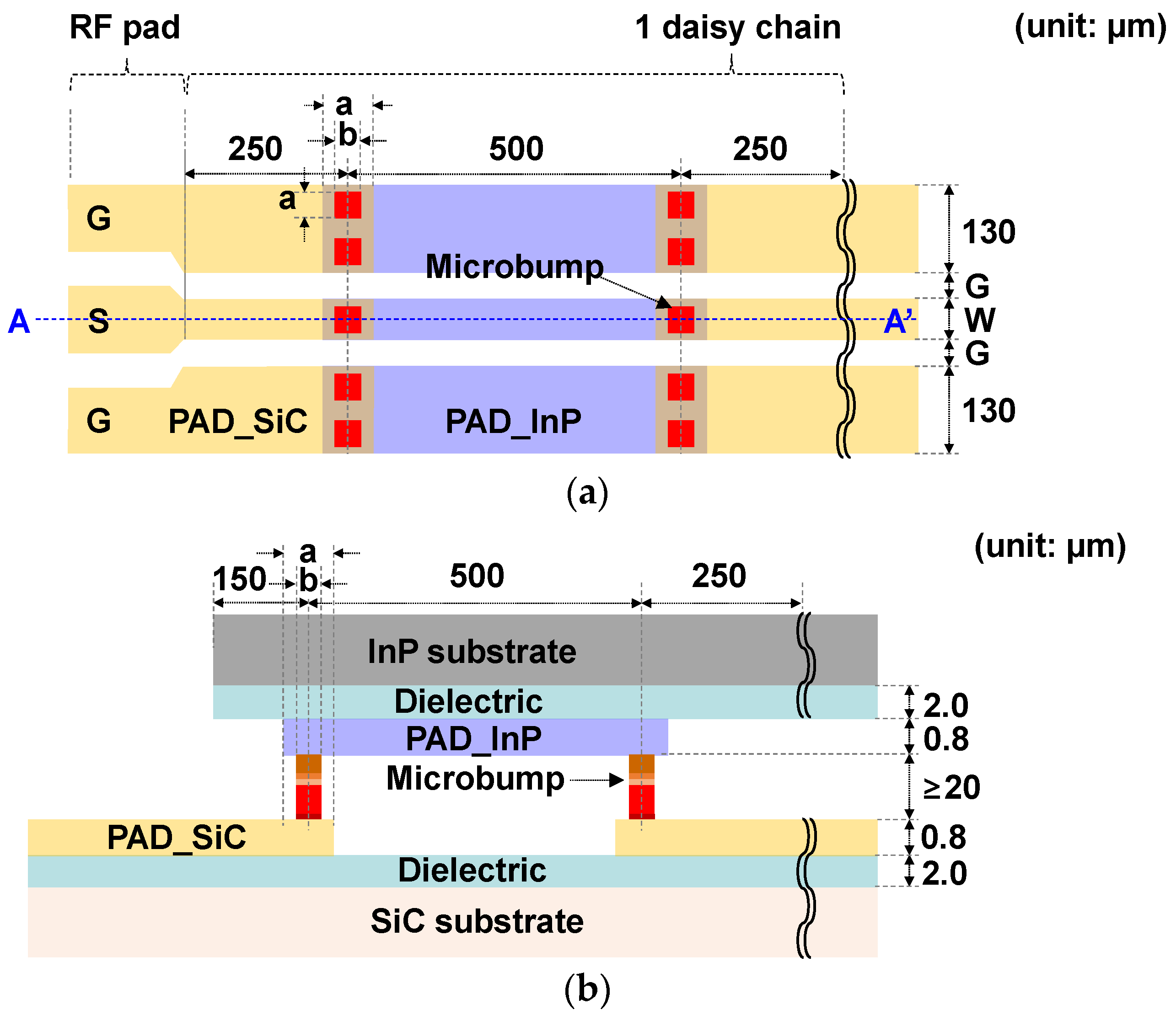
Abstract
1. Introduction
2. Structure Design and Fabrication
2.1. Structure Design of a Flip-Chip μ-Bump Bonding Technology between InP and SiC Substrates
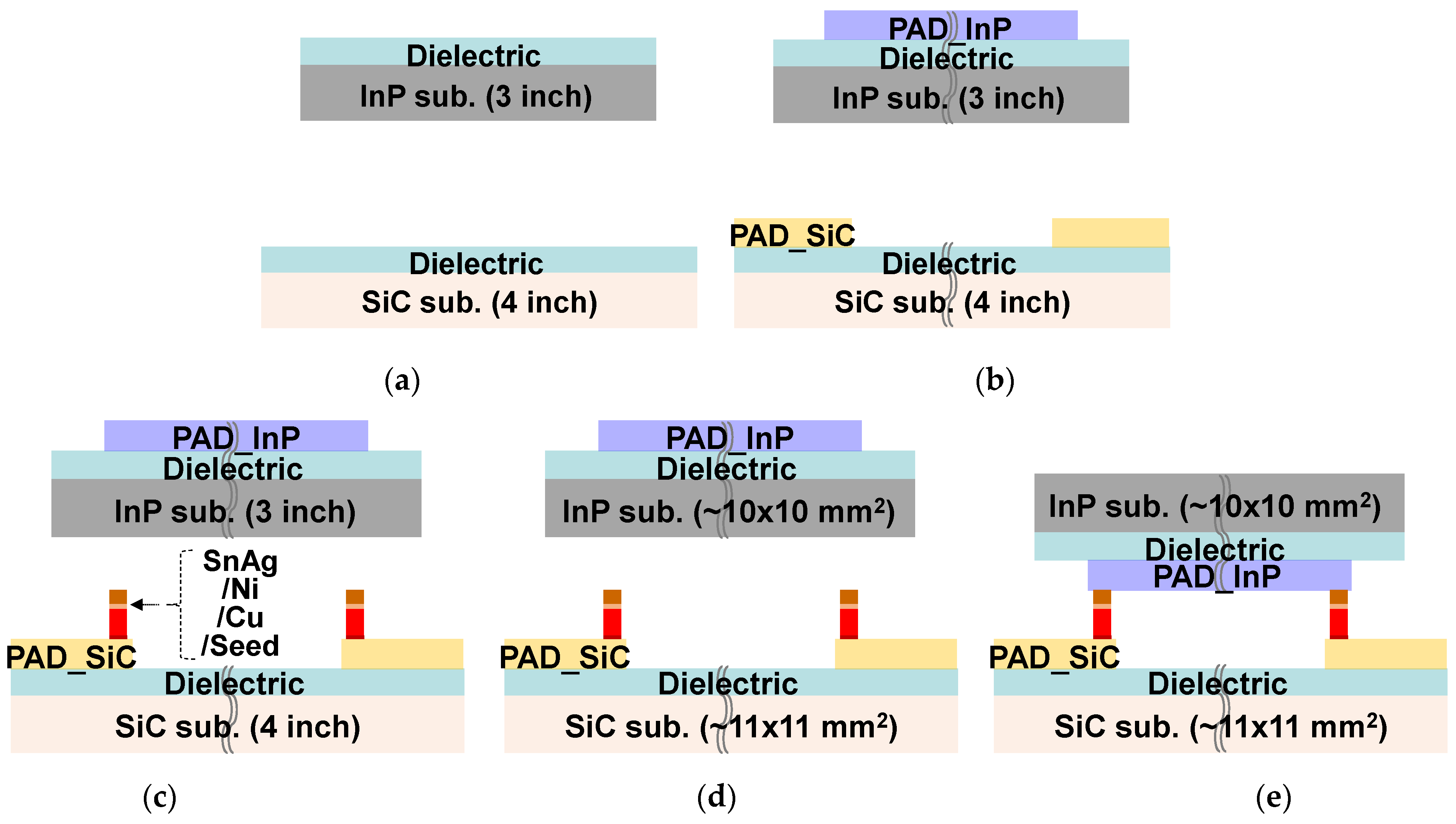
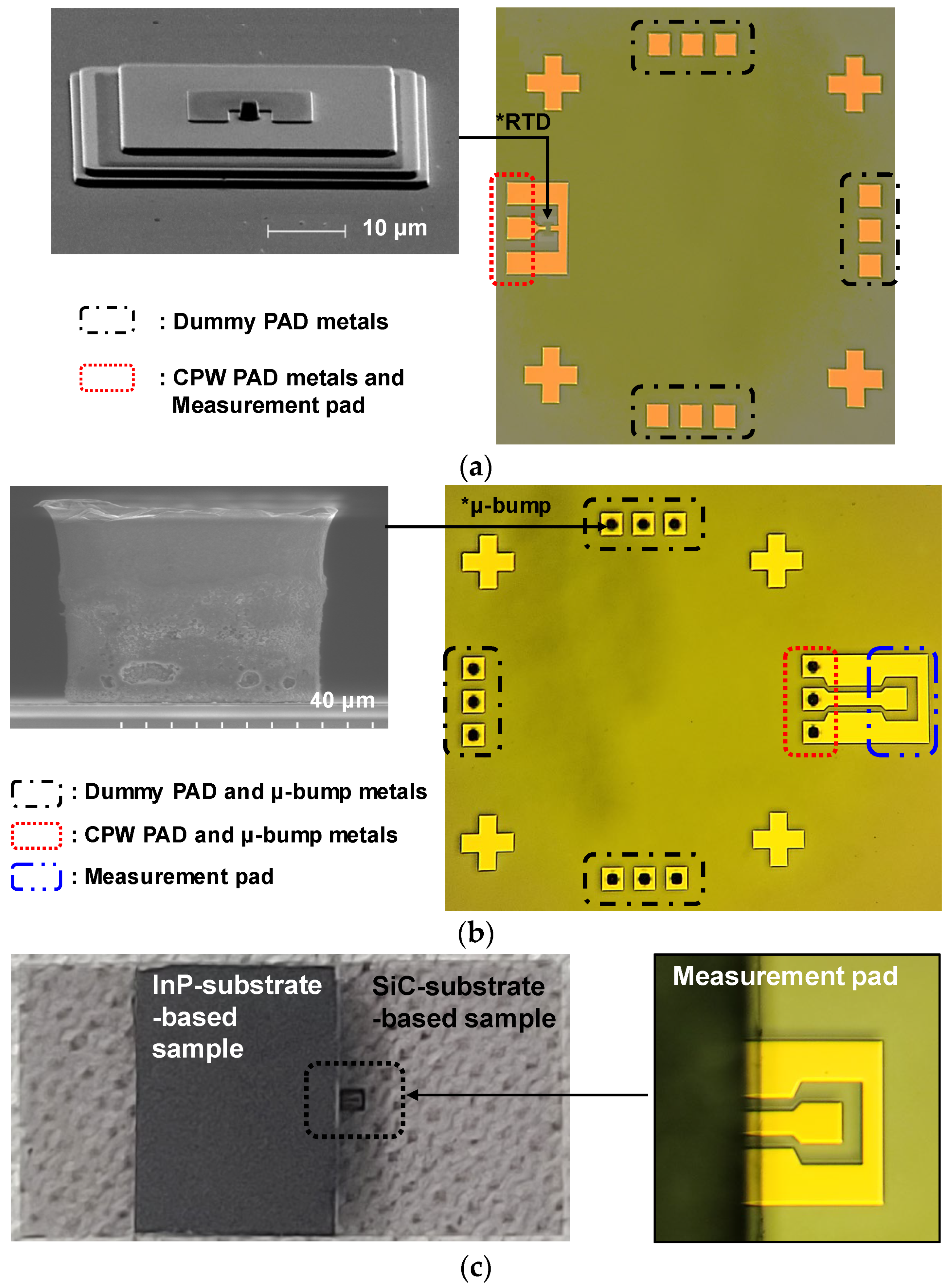
2.2. Fabrication of a Flip-Chip μ-Bump Bonding Process between InP and SiC Substrates
3. Results and Discussion
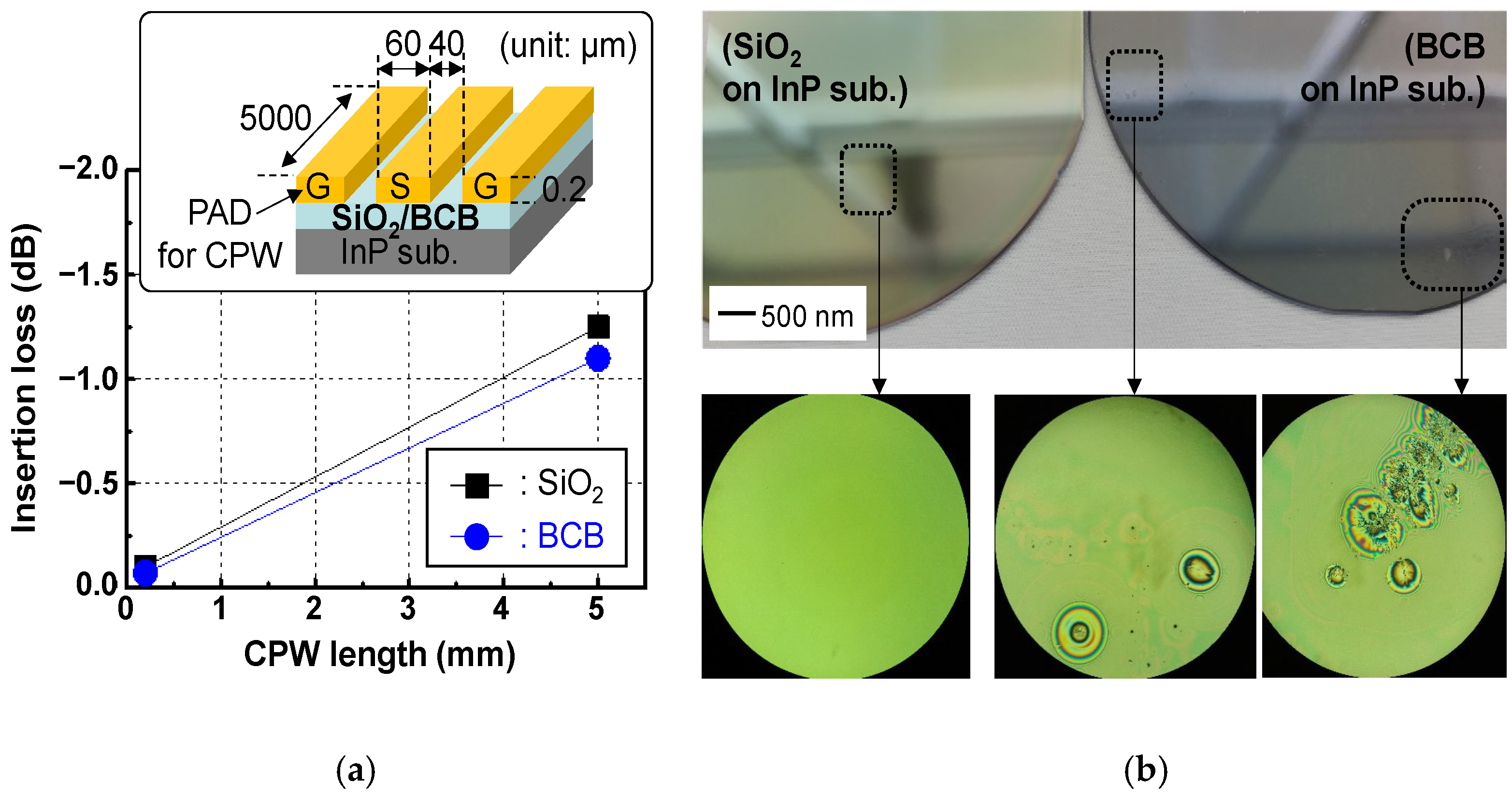
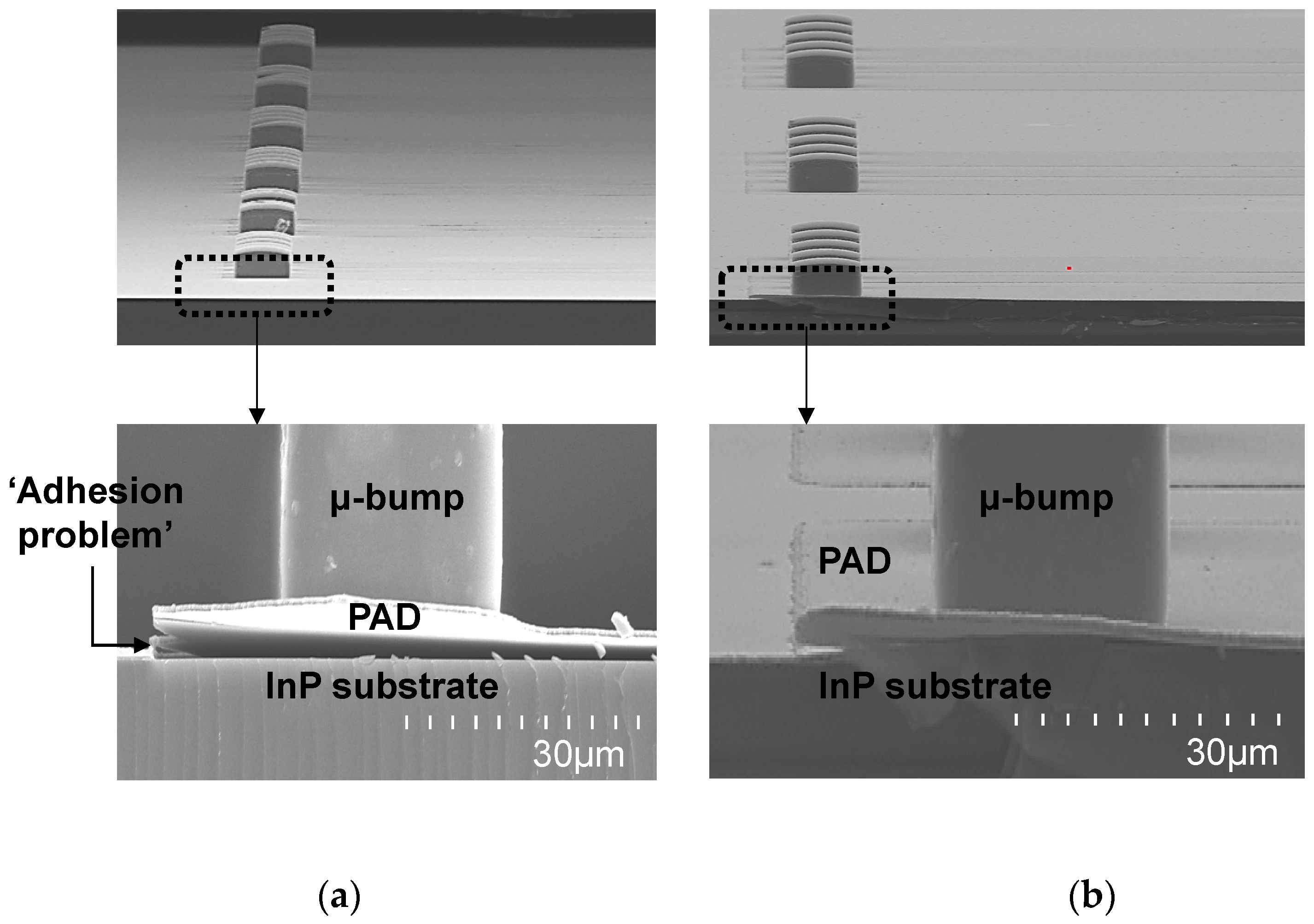
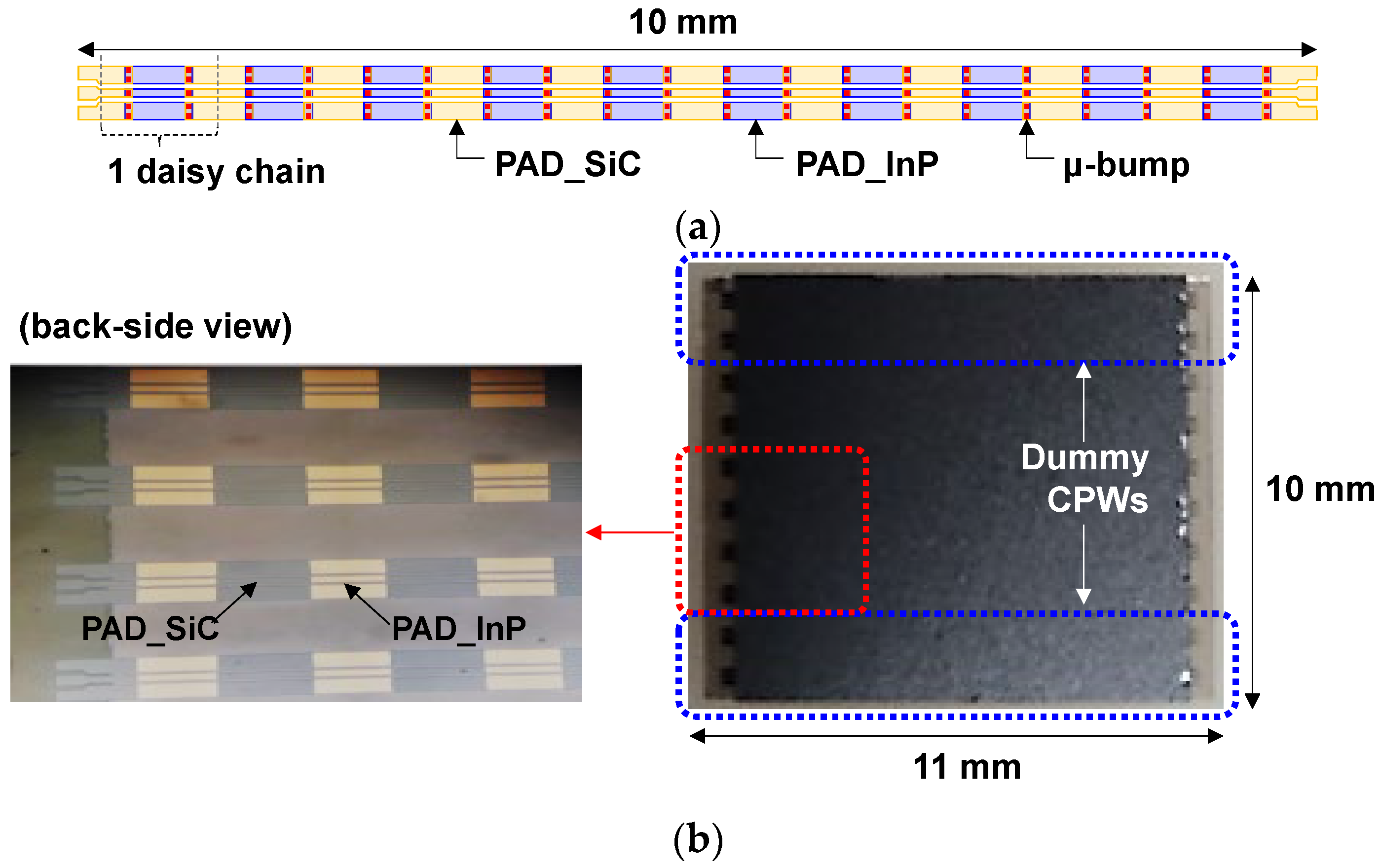
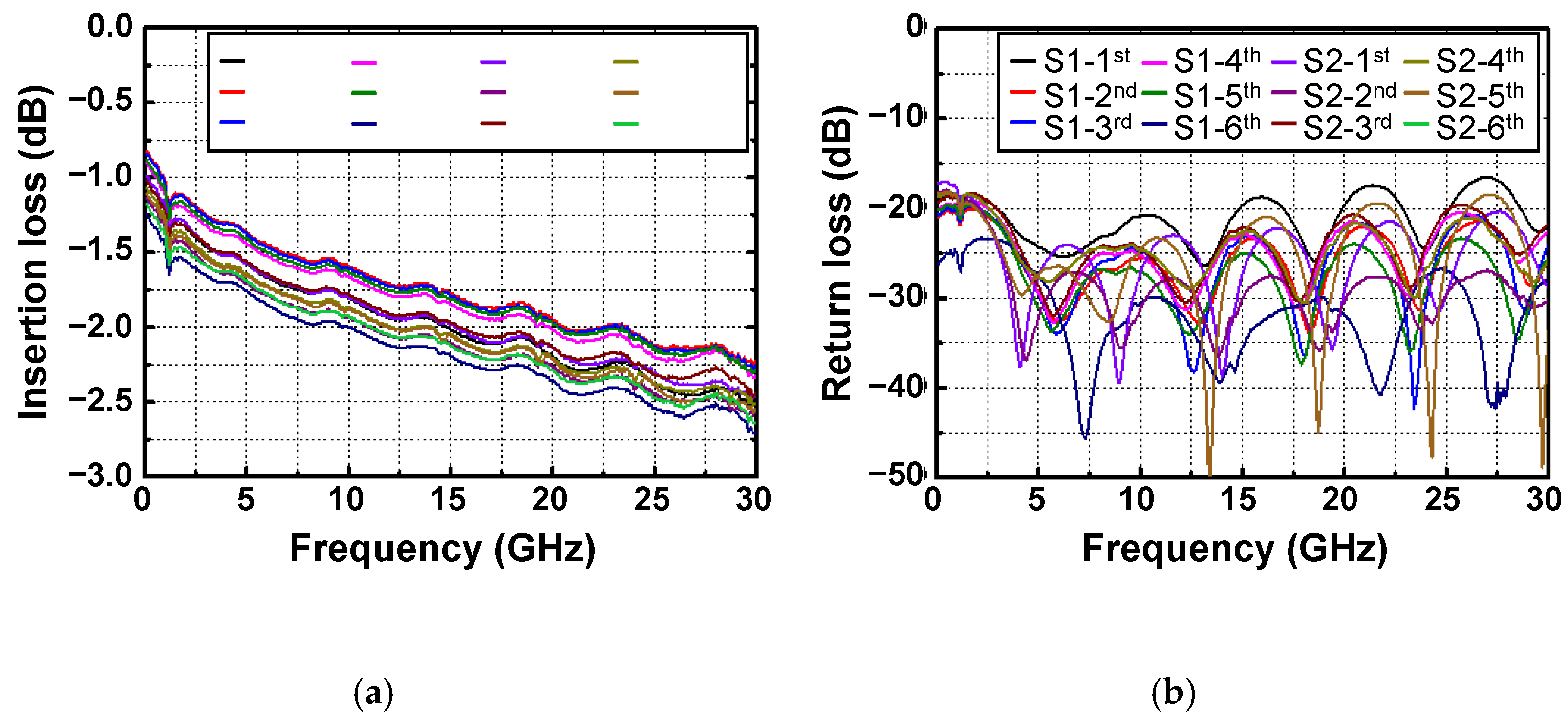
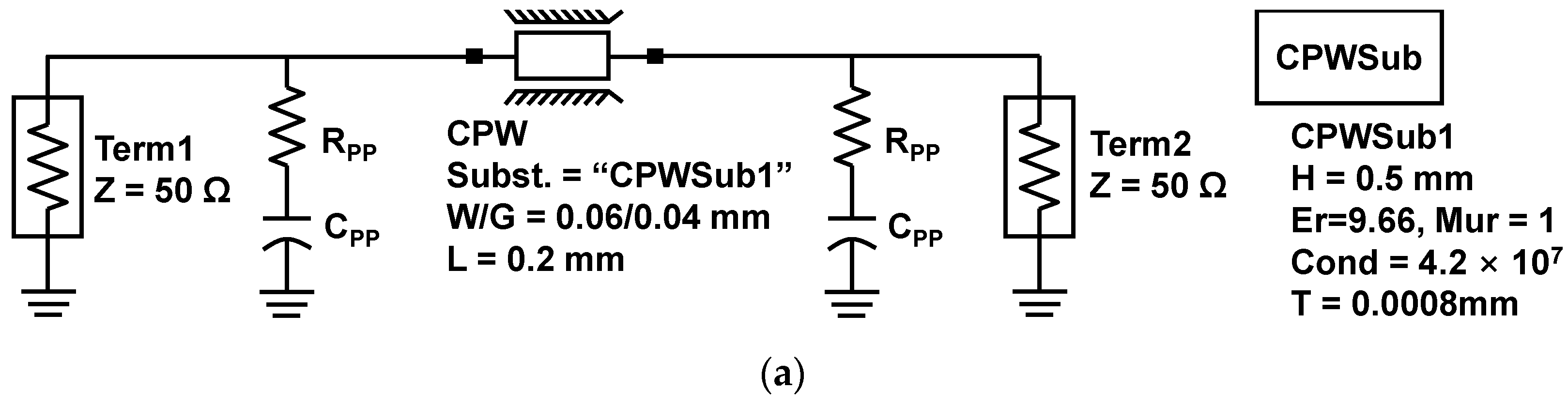
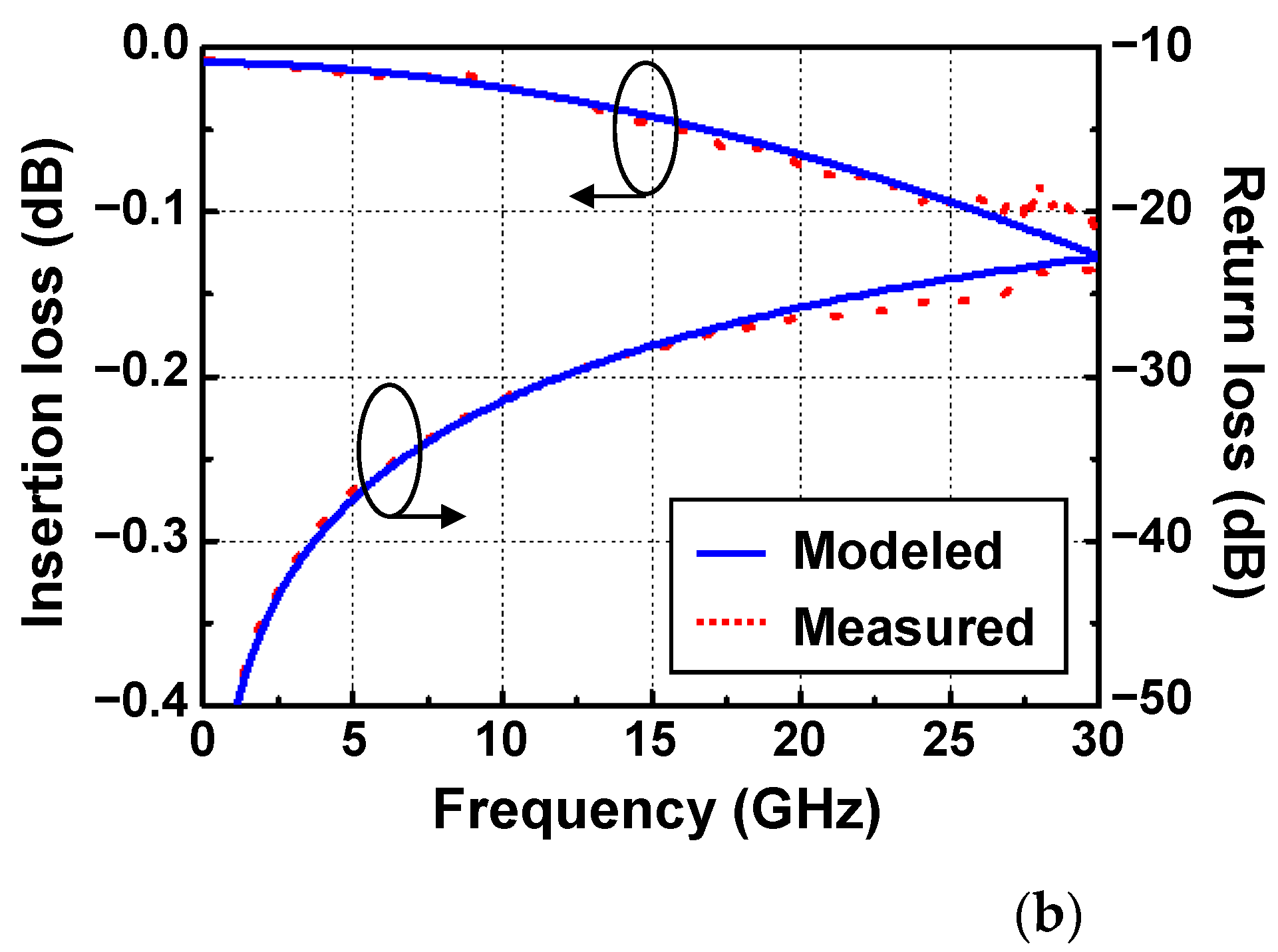
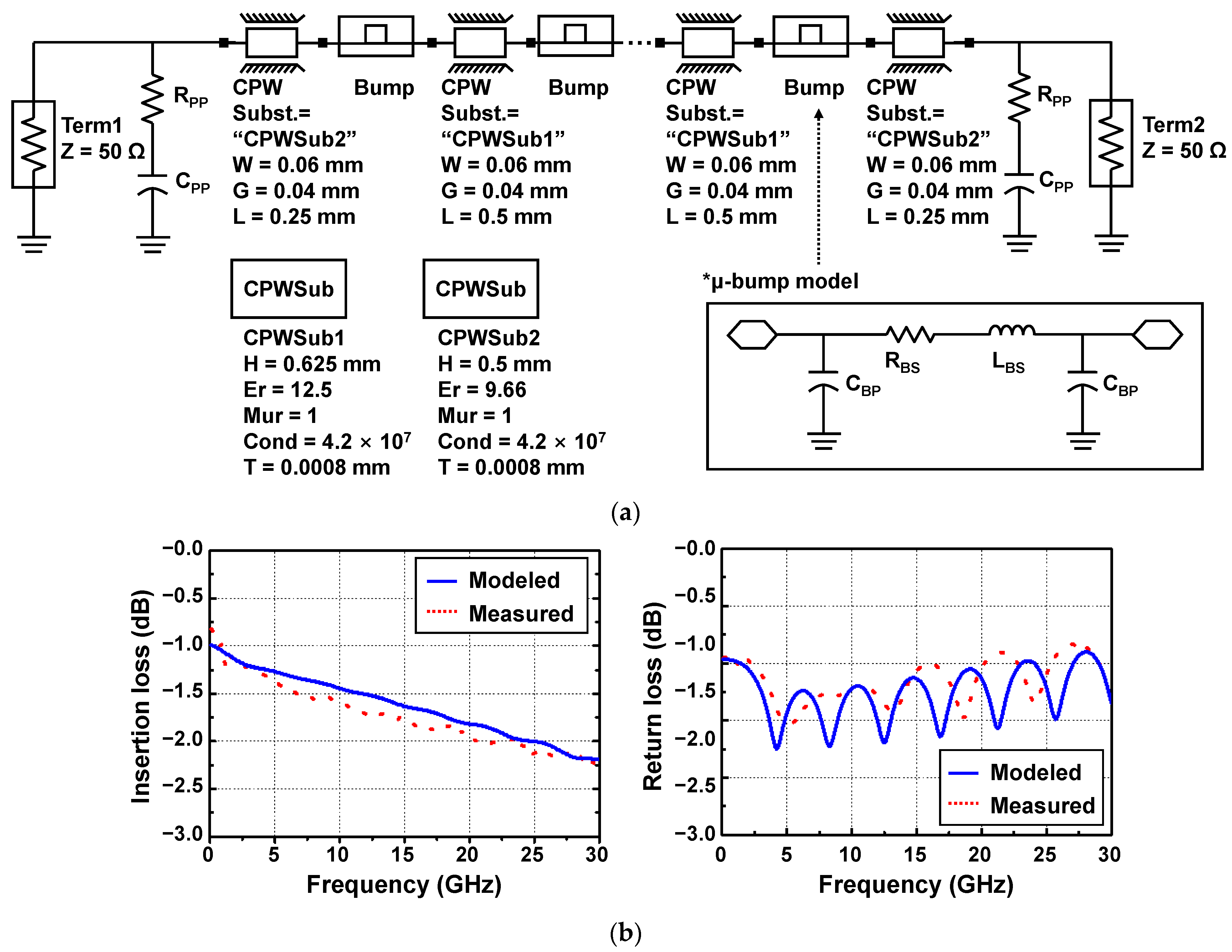
3.1. Performance of Flip-Chip-Bonded InP-to-SiC CPW Lines Consisting of 10 Daisy Chains Interconnected by a Hundred μ-Bumps
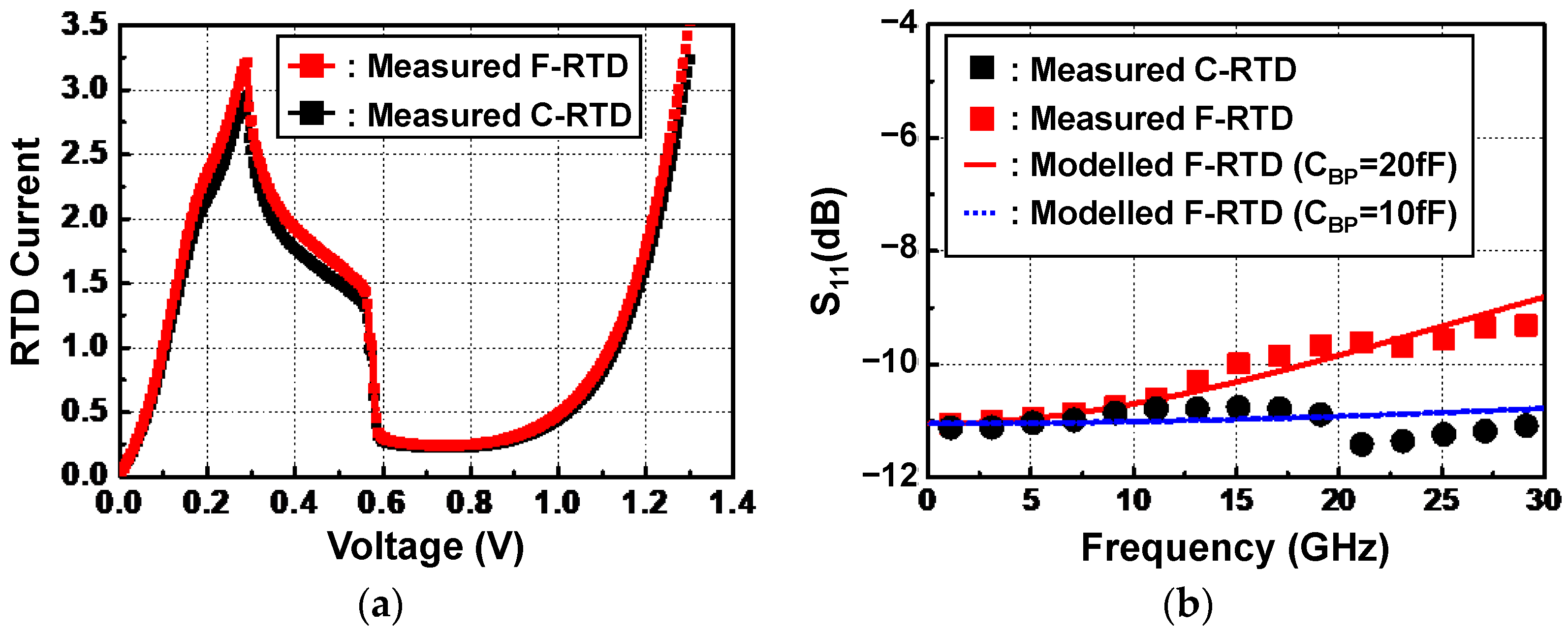
3.2. Application to mmW Device of the Flip-Chip μ-Bump Bonding Technology
4. Conclusions
Author Contributions
Funding
Acknowledgments
Conflicts of Interest
References
- Mei, X.; Yoshida, W.; Lange, M.; Lee, J.; Zhou, J.; Liu, P.; Leong, K.; Zamora, A.; Padilla, J.; Sarkozy, S.; et al. First Demonstration of Amplification at 1 THz Using 25-nm InP High Electron Mobility Transistor Process. IEEE Electron Device Lett. 2015, 36, 327–329. [Google Scholar] [CrossRef]
- Urteaga, M.; Griffith, J.; Young, J.; Pierson, R.; Rowell, P.; Seo, M.; Rodwell, M.J.W. A 130 nm InP HBT Integrated Circuit Technology for THz Electronics. In Proceedings of the 2016 IEEE International Electron Devices Meeting (IEDM), San Francisco, CA, USA, 3–7 December 2016; pp. 711–714. [Google Scholar] [CrossRef]
- Romanczyk, B.; Wienecke, S.; Guidry, M.; Li, H.; Ahmadi, E.; Zheng, X.; Keller, S.; Mishra, U.K. Demonstration of Constant 8 W/mm Power Density at 10, 30, and 94 GHz in State-of-the-Art Millimeter-Wave N-Polar GaN MISHEMTs. IEEE Trans. Electron Devices 2018, 65, 45–50. [Google Scholar] [CrossRef]
- Green, D.S.; Dohrman, C.L.; Demmin, J.; Zheng, Y.; Chang, T.-H. A Revolution on the Horizon from DARPA: Heterogeneous Integration for Revolutionary Microwave\/Millimeter-Wave Circuits at DARPA: Progress and Future Directions. IEEE Microw. Mag. 2017, 18, 44–59. [Google Scholar] [CrossRef]
- Carter, A.; Urteaga, M. 3D integration unites InP, GaN and silicon CMOS. Compd. Semicond. 2018, 24, 50–53. Available online: https://compoundsemiconductor.net/article/104207/3D_Integration_Unites_InP_GaN_And_Silicon_CMOS (accessed on 15 June 2021).
- Micromachines Lee, J.; Roh, K.; Lim, S.-K.; Kim, Y. Sidewall Slope Control of InP Via Holes for 3D Integration. Micromachines 2021, 12, 89. [Google Scholar] [CrossRef] [PubMed]
- Scott, D.; Monier, C.; Wang, S.; Radisic, V.; Nguyen, P.; Cavus, A.; Deal, W.; Gutierrez-Aitken, A. InP HBT Transferred to Higher Thermal Conductivity Substrate. IEEE Electron Device Lett. 2012, 33, 507–509. [Google Scholar] [CrossRef]
- Watanabe, M.; Yanagisawa, M.; Uesaka, K.; Ekawa, M.; Shoji, H. InP-DHBT Fabricated on High Heat Dissipation SiC Wafer Using Atomic Diffusion Bonding. SEI Tech. Rev. 2016, 83, 45–49. [Google Scholar]
- Shiratori, Y.; Hoshi, T.; Ida, M.; Higurashi, E.; Matsuzaki, H. High-Speed InP/InGaAsSb DHBT on High-Thermal-Conductivity SiC Substrate. IEEE Electron Device Lett. 2018, 39, 807–810. [Google Scholar] [CrossRef]
- Takenaka, M.; Takagi, S. InP-based photonic integrated circuit platform on SiC wafer. Opt. Express 2017, 25, 29993–30000. [Google Scholar] [CrossRef] [PubMed]
- Wu, L.; JiaYun, D.; Cheng, W.; Kong, Y.; Chen, T.; Zhang, T. Heterogeneous Integration of InP DHBT and Si CMOS by 30μm Pitch Au-In Microbumps. In Proceedings of the 2021 Electron Devices Technology and Manufacturing Conference (EDTM), Chengdu, China, 8–11 April 2021; pp. 1–3. [Google Scholar] [CrossRef]
- Geum, D.-M.; Kim, S.; Lee, S.; Lim, D.; Kim, H.-J.; Choi, C.; Kim, S.-H. Monolithic 3D Integration of InGaAs Photodetectors on Si MOSFETs Using Sequential Fabrication Process. IEEE Electron Device Lett. 2020, 41, 433–436. [Google Scholar] [CrossRef]
- Li, J.; Zhang, Y.; Zhang, H.; Chen, Z.; Zhou, C.; Liu, X.; Zhu, W. The thermal cycling reliability of copper pillar solder bump in flip chip via thermal compression bonding. Microelectron. Reliab. 2020, 104, 113543. [Google Scholar] [CrossRef]
- Koh, W.; Lin, B.; Tai, J. Copper Pillar Bump Technology Progress Overview. In Proceedings of the 2011 International Conference on Electronic Packaging Technology & High Density Packaging, Shanghai, China, 8–11 August 2011; pp. 1–5. [Google Scholar] [CrossRef]
- Lee, J.; Lee, C.; Kim, C.; Kalchuri, S. Micro Bump System for 2nd Generation Silicon Interposer with GPU and High Bandwidth Memory (HBM) Concurrent Integration. In Proceedings of the 2018 IEEE 68th Electronic Components and Technology Conference, San Diego, CA, USA, 29 May 2018–1 June 2018; pp. 607–612. [Google Scholar] [CrossRef]
- Mori, K.; Ono, Y.; Watanabe, S.; Ishikawa, T.; Sugiyama, M.; Imasu, S.; Ochiai, T.; Mori, R.; Kida, T.; Hashimoto, T.; et al. High Density and Reliable Packaging Technology with Non Conductive Film for 3D/TSV. In Proceedings of the 2013 IEEE International 3D Systems Integration Conference (3DIC), San Francisco, CA, USA, 2–4 October 2013; pp. 1–7. [Google Scholar] [CrossRef]
- Urteaga, M.; Carter, A.; Griffith, Z.; Pierson, R.; Bergman, J.; Arias, A.; Rowell, P.; Hacker, J.; Brar, B.; Rodwell, M.J.W. THz Bandwidth InP HBT Technologies and Heterogeneous Integration with Si CMOS. In Proceedings of the 2016 IEEE Bipolar/BiCMOS Circuits and Technology Meeting (BCTM), New Brunswick, NJ, USA, 25–27 September 2016; pp. 35–41. [Google Scholar] [CrossRef]
- Weimann, N.; Monayakul, S.; Sinha, S.; Schmückle, F.-J.; Hrobak, M.; Stoppel, D.; John, W.; Krüger, O.; Doerner, R.; Janke, B.; et al. Manufacturable Low-Cost Flip-Chip Mounting Technology for 300–500-GHz Assemblies. IEEE Trans. Compon. Packag. Manuf. Technol. 2017, 7, 494–501. [Google Scholar] [CrossRef]
- Lahiji, R.R.; Sharifi, H.; Katehi, L.P.B.; Mohammadi, S. 3-D CMOS Circuits Based on Low-Loss Vertical Interconnects on Parylene-N. IEEE Trans. Microw. Theory Tech. 2010, 58, 48–56. [Google Scholar] [CrossRef][Green Version]
- Watanabe, A.O.; Ali, M.; Sayeed, S.Y.B.; Tummala, R.R.; Pulugurtha, M.R. A Review of 5G Front-End Systems Package Integration. IEEE Trans. Compon. Package. Manuf. Technol. 2021, 11, 118–133. [Google Scholar] [CrossRef]
- Zhang, Q.X.; Yu, A.B.; Yang, R.; Li, H.Y.; Guo, L.H.; Liao, E.B.; Tang, M.; Lo, G.-Q.; Balasubramanian, N.; Kwong, D.-L. Integration of RF MEMS and CMOS IC on a Printed Circuit Board for a Compact RF System Application Based on Wafer Transfer. IEEE Trans. Electron Devices 2008, 55, 2484–2491. [Google Scholar] [CrossRef]
- Staiculescu, D.; Sutono, A.; Laskar, J. Wideband Scalable Electrical Model for Microwave/Millimeter Wave Flip Chip Interconnects. IEEE Trans. Adv. Packag. 2001, 24, 255–259. [Google Scholar] [CrossRef]
- Maekawa, T.; Kanaya, H.; Suzuki, S.; Asada, M. Oscillation up to 1.92 THz in resonant tunneling diode by reduced conduction loss. Appl. Phys. Express 2016, 9, 024101. [Google Scholar] [CrossRef]
- Lee, J.; Kim, M.; Lee, J. 692 GHz High-Efficiency Compact-Size InP-Based Fundamental RTD Oscillator. IEEE Trans. THz Sci. Technol. 2021, 11, 716–719. [Google Scholar] [CrossRef]
- Lee, J.; Kim, M.; Park, J.; Lee, J. 225 GHz triple-push RTD oscillator with 0.5 mW dc-power consumption. IET Circuits Devices Syst. 2020, 14, 209–215. [Google Scholar] [CrossRef]


Publisher’s Note: MDPI stays neutral with regard to jurisdictional claims in published maps and institutional affiliations. |
© 2022 by the authors. Licensee MDPI, Basel, Switzerland. This article is an open access article distributed under the terms and conditions of the Creative Commons Attribution (CC BY) license (https://creativecommons.org/licenses/by/4.0/).
Share and Cite
Lee, J.; Lee, J.Y.; Song, J.; Sim, G.; Ko, H.; Kong, S.H. Implementation of Flip-Chip Microbump Bonding between InP and SiC Substrates for Millimeter-Wave Applications. Micromachines 2022, 13, 1072. https://doi.org/10.3390/mi13071072
Lee J, Lee JY, Song J, Sim G, Ko H, Kong SH. Implementation of Flip-Chip Microbump Bonding between InP and SiC Substrates for Millimeter-Wave Applications. Micromachines. 2022; 13(7):1072. https://doi.org/10.3390/mi13071072
Chicago/Turabian StyleLee, Jongwon, Jae Yong Lee, Jonghyun Song, Gapseop Sim, Hyoungho Ko, and Seong Ho Kong. 2022. "Implementation of Flip-Chip Microbump Bonding between InP and SiC Substrates for Millimeter-Wave Applications" Micromachines 13, no. 7: 1072. https://doi.org/10.3390/mi13071072
APA StyleLee, J., Lee, J. Y., Song, J., Sim, G., Ko, H., & Kong, S. H. (2022). Implementation of Flip-Chip Microbump Bonding between InP and SiC Substrates for Millimeter-Wave Applications. Micromachines, 13(7), 1072. https://doi.org/10.3390/mi13071072