
A Direct n+-Formation Process by Magnetron Sputtering an Inter-Layer Dielectric for Self-Aligned Coplanar Indium Gallium Zinc Oxide Thin-Film Transistors

Abstract
:1. Introduction
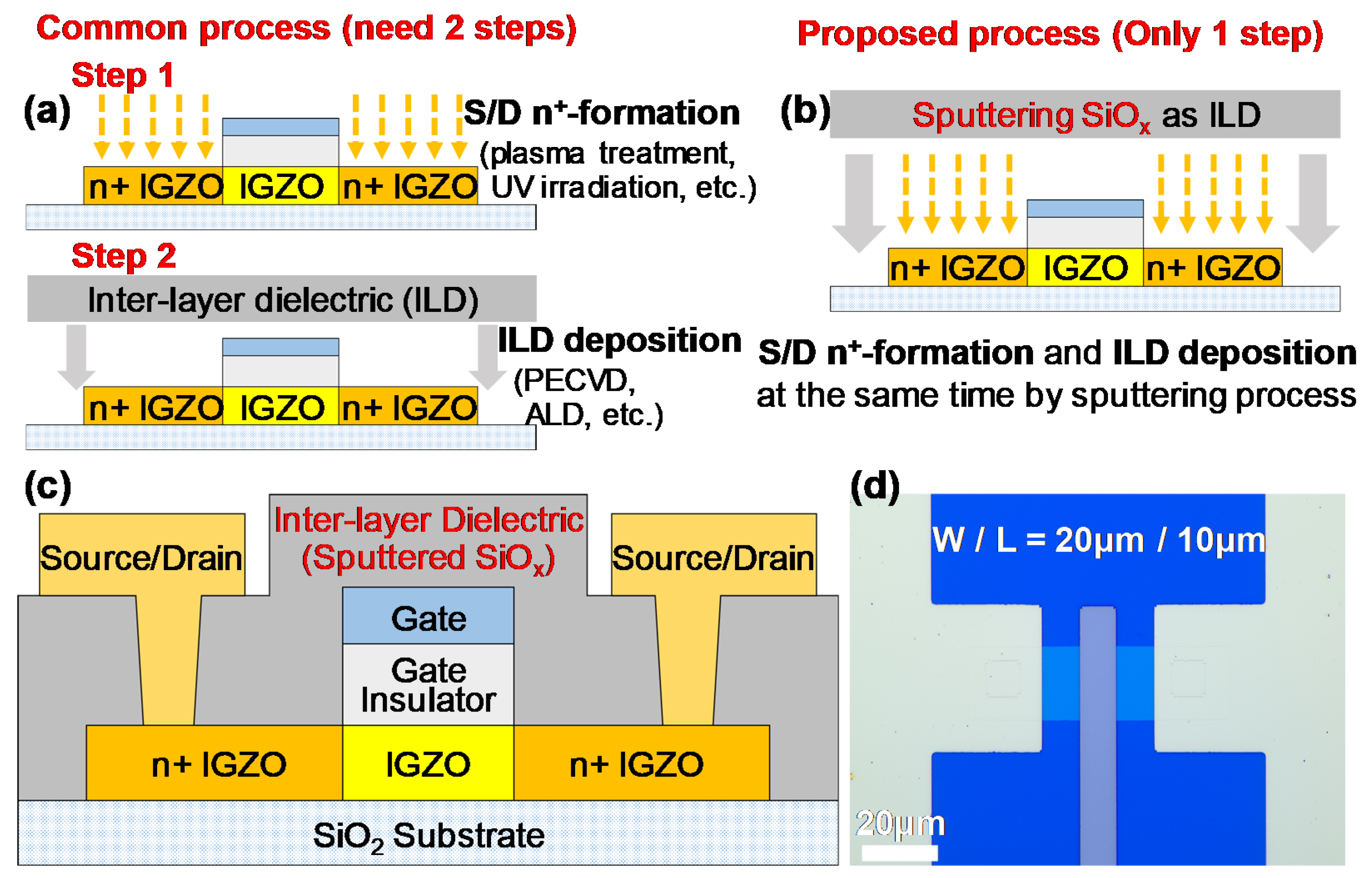
2. Experiment
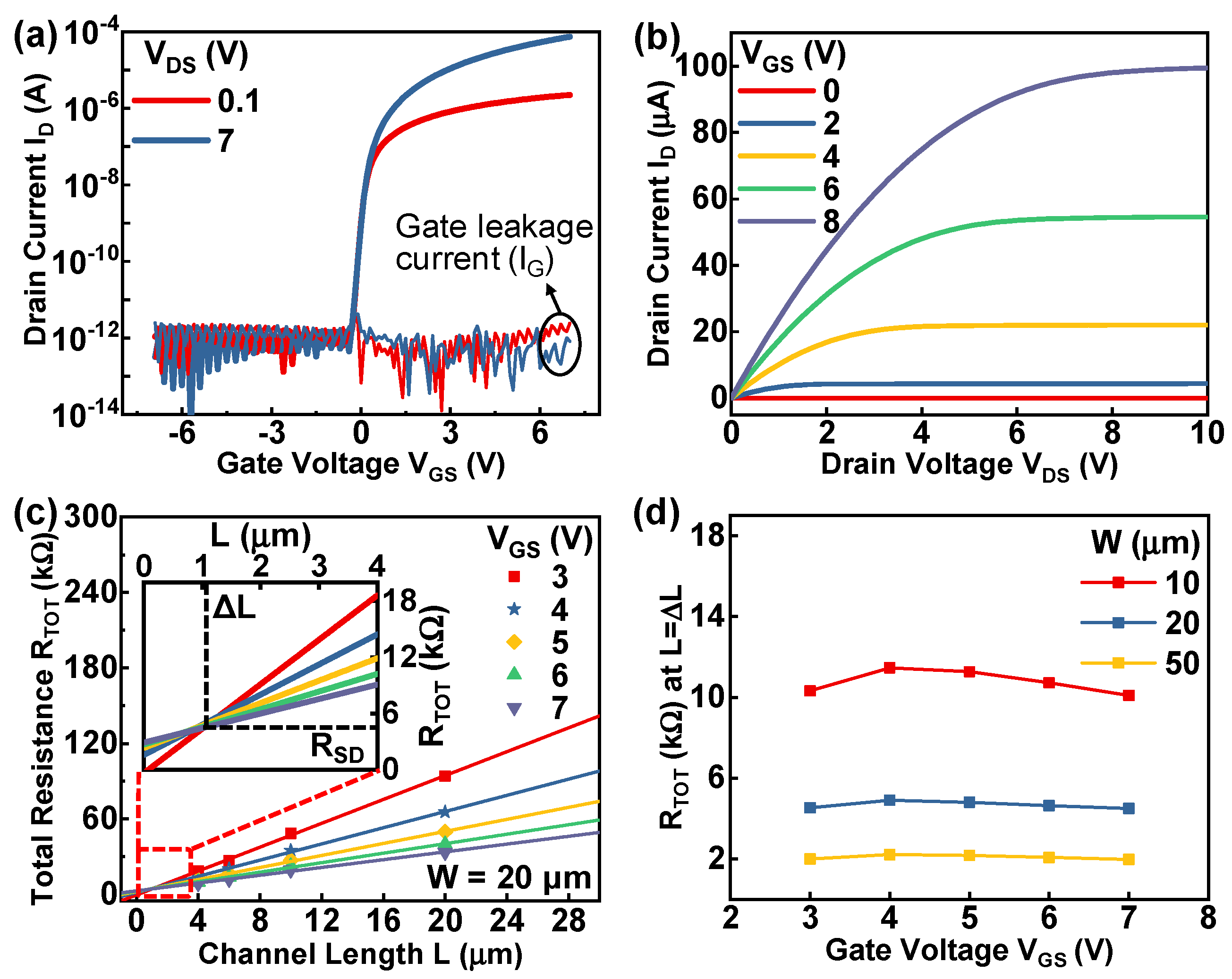
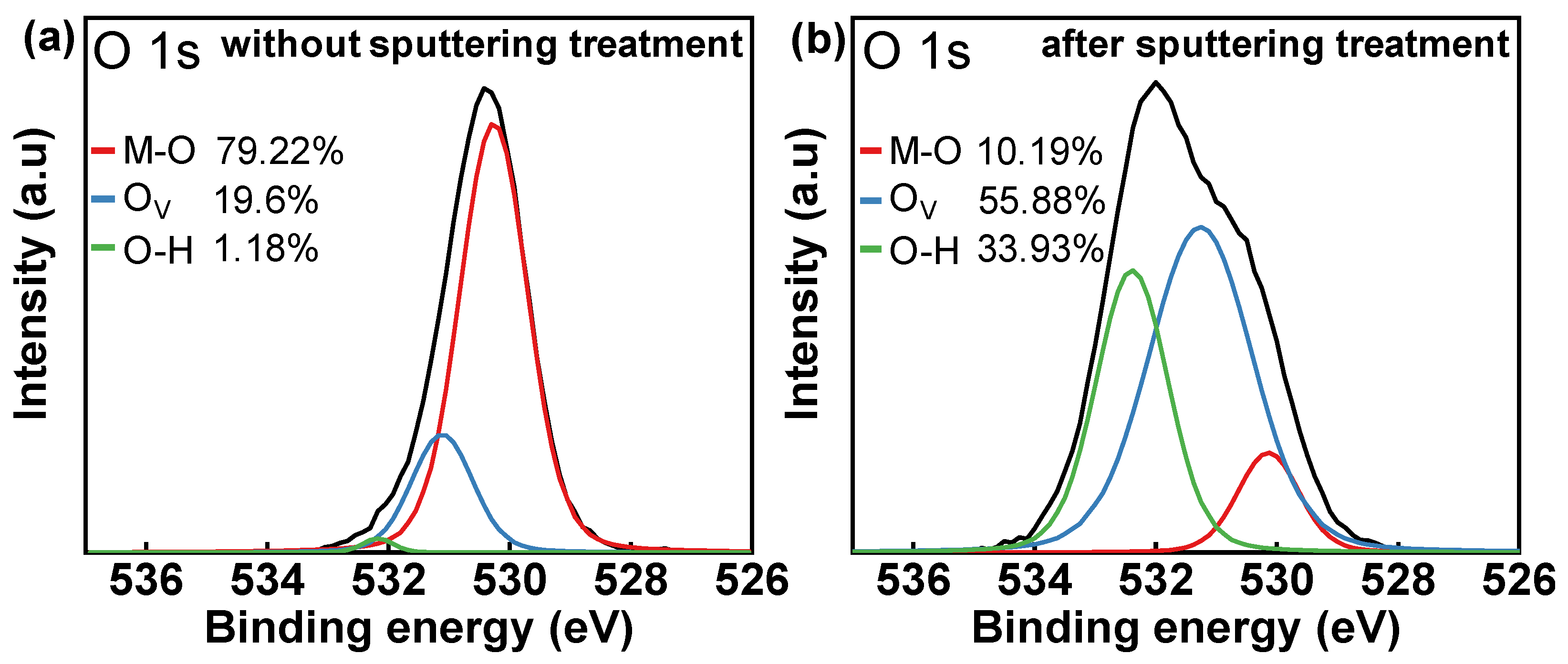
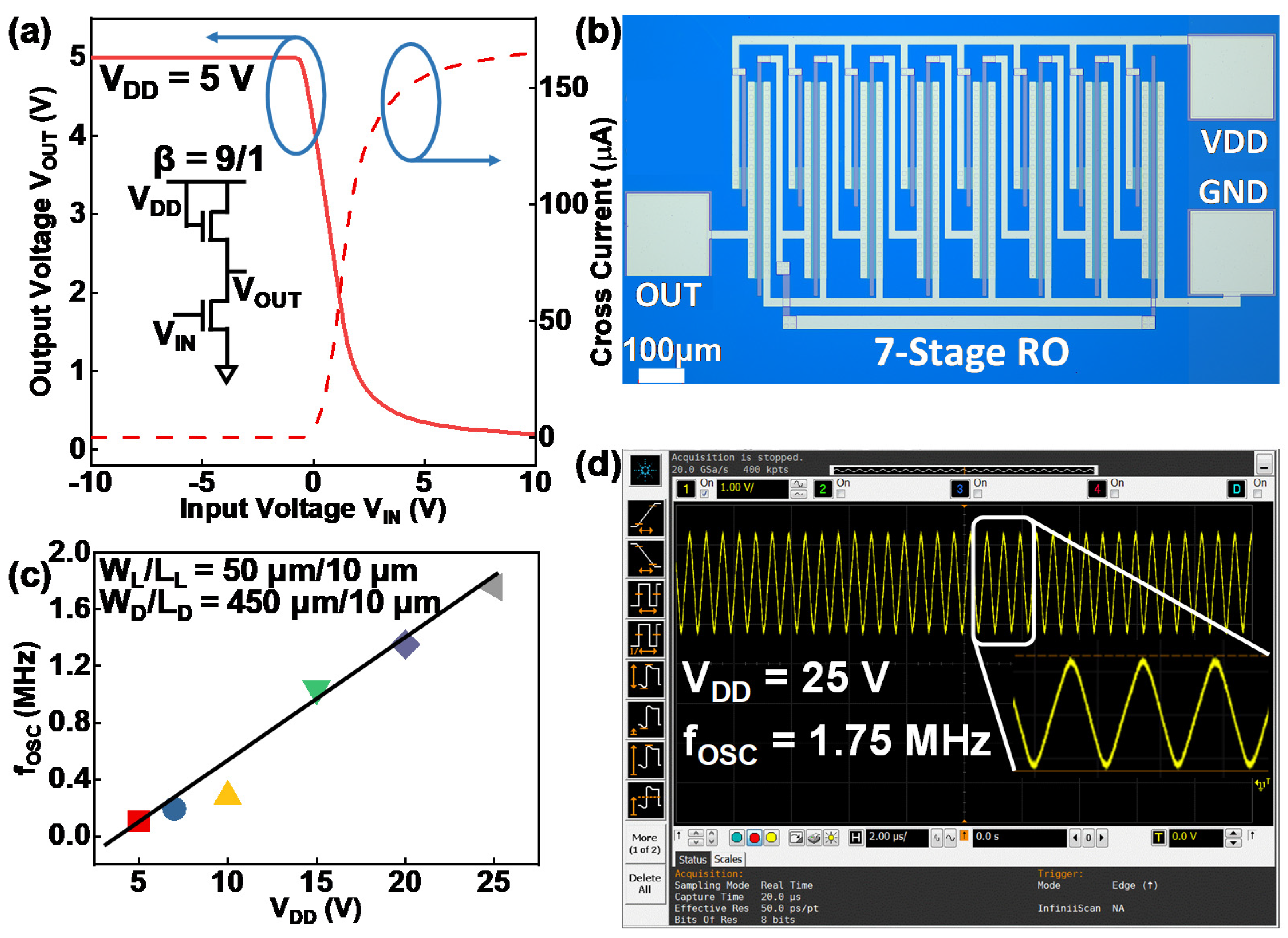
3. Results and Discussion
4. Conclusions
Author Contributions
Funding
Data Availability Statement
Conflicts of Interest
References
- Tai, A.-H.; Yen, C.-C.; Chen, T.-L.; Chou, C.-H.; Liu, C.W. Mobility Enhancement of Back-Channel-Etch Amorphous InGaZnO TFT by Double Layers with Quantum Well Structures. IEEE Trans. Electron. Devices 2019, 66, 4188–4192. [Google Scholar] [CrossRef]
- Koretomo, D.; Toda, T.; Matsuda, T.; Kimura, M.; Furuta, M. Anomalous Increase in Field-Effect Mobility in In–Ga–Zn–O Thin-Film Transistors Caused by Dry-Etching Damage through Etch-Stop Layer. IEEE Trans. Electron. Devices 2016, 63, 2785–2789. [Google Scholar] [CrossRef]
- Ha, C.; Lee, H.-J.; Kwon, J.-W.; Seok, S.-Y.; Ryoo, C.-I.; Yun, K.-Y.; Kim, B.-C.; Shin, W.-S.; Cha, S.-Y. 69.2:Distinguished Paper: High Reliable a-IGZO TFTs with Self-Aligned Coplanar Structure for Large-Sized Ultrahigh-Definition OLED TV. SID Symp. Dig. Tech. Pap. 2015, 46, 1020–1022. [Google Scholar] [CrossRef]
- Park, J.-S.; Jeong, J.K.; Mo, Y.-G.; Kim, H.D.; Kim, S.-I. Improvements in the device characteristics of amorphous indium gallium zinc oxide thin-film transistors by Ar plasma treatment. Appl. Phys. Lett. 2007, 90, 262106. [Google Scholar] [CrossRef]
- Du Ahn, B.; Shin, H.S.; Kim, H.J.; Park, J.-S.; Jeong, J.K. Comparison of the effects of Ar and H2 plasmas on the performance of homojunctioned amorphous indium gallium zinc oxide thin film transistors. Appl. Phys. Lett. 2008, 93, 203506. [Google Scholar] [CrossRef]
- Ryu, S.-M.; Kim, M.-H.; Jeon, S.-H.; Lim, J.-H.; Choi, D.-K. Self-Aligned Coplanar Top Gate In-Ga-ZnO Thin-Film Transistors Exposed to Various DUV Irradiation Energies. IEEE Trans. Electron. Devices 2016, 63, 3123–3127. [Google Scholar] [CrossRef]
- Hong, S.-Y.; Kim, H.-J.; Kim, D.-H.; Jeong, H.-Y.; Song, S.-H.; Cho, I.-T.; Noh, J.; Yun, P.S.; Lee, S.-W.; Park, K.-S.; et al. Study on the Lateral Carrier Diffusion and Source-Drain Series Resistance in Self-Aligned Top-Gate Coplanar InGaZnO Thin-Film Transistors. Sci. Rep. 2019, 9, 6588. [Google Scholar] [CrossRef]
- On, N.; Kim, B.K.; Lee, S.; Kim, E.H.; Lim, J.H.; Jeong, J.K. Hot Carrier Effect in Self-Aligned In–Ga–Zn–O Thin-Film Transistors with Short Channel Length. IEEE Trans. Electron. Devices 2020, 67, 5544–5551. [Google Scholar] [CrossRef]
- Kim, H.-E.; Furuta, M.; Yoon, S.-M. A Facile Doping Process of the Organic Inter-Layer Dielectric for Self-Aligned Coplanar In-Ga-Zn-O Thin-Film Transistors. IEEE Electron. Device Lett. 2020, 41, 393–396. [Google Scholar] [CrossRef]
- Choi, S.-H.; Han, M.-K. Effect of Deposition Temperature of SiOx Passivation Layer on the Electrical Performance of a-IGZO TFTs. IEEE Electron. Device Lett. 2012, 33, 396–398. [Google Scholar] [CrossRef]
- Yang, X.; Kim, D.-P.; Um, D.-S.; Kim, G.-H.; Kim, C.-I. Temperature dependence on dry etching of Al2O3 thin films in BCl3/Cl2/Ar plasma. J. Vac. Sci. Technol. A Vac. Surf. Films 2009, 27, 821–825. [Google Scholar] [CrossRef]
- Joo, Y.-H.; Woo, J.-C.; Kim, C.-I. A Study of the Surface Chemical Reactions on IGZO Thin Film in BCl3/Ar Inductively Coupled Plasma. J. Electrochem. Soc. 2012, 159, D190–D195. [Google Scholar] [CrossRef]
- Shi, X.; Lu, C.; Duan, X.; Chen, Q.; Ji, H.; Su, Y.; Chuai, X.; Liu, D.; Zhao, Y.; Yang, G.; et al. Study of Positive-Gate-Bias-Induced Hump Phenomenon in Amorphous Indium–Gallium–Zinc Oxide Thin-Film Transistors. IEEE Trans. Electron. Devices 2020, 67, 1606–1612. [Google Scholar] [CrossRef]
- Sato, A.; Abe, K.; Hayashi, R.; Kumomi, H.; Nomura, K.; Kamiya, T.; Hirano, M.; Hosono, H. Amorphous In–Ga–Zn–O coplanar homojunction thin-film transistor. Appl. Phys. Lett. 2009, 94, 133502. [Google Scholar] [CrossRef] [Green Version]
- Wang, W.; Li, L.; Ji, Z.; Lu, C.; Liu, Y.; Lv, H.; Xu, G.; Liu, M. Analysis of the temperature dependent contact resistance in amorphous InGaZnO thin film transistors. In Proceedings of the 2015 28th International Vacuum Nanoelectronics Conference (IVNC), Guangzhou, China, 13–17 July 2015; pp. 206–207. [Google Scholar] [CrossRef]
- Du Ahn, B.; Shin, H.S.; Kim, G.H.; Park, J.-S.; Kim, H.J. A Novel Amorphous InGaZnO Thin Film Transistor Structure without Source/Drain Layer Deposition. Jpn. J. Appl. Phys. 2009, 48, 03B019. [Google Scholar] [CrossRef]
- Kim, M.-M.; Ryu, S.-M.; Lim, J.H.; Choi, D.-K. Coplanar homojunction a-InGaZnO thin film transistor fabricated using ultraviolet irradiation. RSC Adv. 2015, 5, 82947–82951. [Google Scholar] [CrossRef]
- Kamiya, T.; Nomura, K.; Hosono, H. Present status of amorphous In-Ga-Zn-O thin-film transistors. Sci. Technol. Adv. Mater. 2010, 11, 044305. [Google Scholar] [CrossRef]
- Jianke, Y.; Ningsheng, X.; Shaozhi, D.; Jun, C.; Juncong, S.; Shieh, H.D.; Po-Tsun, L.; Yi-Pai, H. Electrical and Photosensitive Characteristics of a-IGZO TFTs Related to Oxygen Vacancy. IEEE Trans. Electron. Devices 2011, 58, 1121–1126. [Google Scholar] [CrossRef]
- Chen, M.; Pei, Z.; Sun, C.; Wen, L.; Wang, X. Surface characterization of transparent conductive oxide Al-doped ZnO films. J. Cryst. Growth 2000, 220, 254–262. [Google Scholar] [CrossRef]
- Saito, N.; Miura, K.; Ueda, T.; Tezuka, T.; Ikeda, K. High-Mobility and H2-Anneal Tolerant InGaSiO/InGaZnO/InGaSiO Double Hetero Channel Thin Film Transistor for Si-LSI Compatible Process. IEEE J. Electron. Devices Soc. 2018, 6, 500–505. [Google Scholar] [CrossRef]
- Kim, J.; Bang, S.; Lee, S.; Shin, S.; Park, J.; Seo, H.; Jeon, H. A study on H2 plasma treatment effect on a-IGZO thin film transistor. J. Mater. Res. 2012, 27, 2318–2325. [Google Scholar] [CrossRef] [Green Version]
- Seok, M.J.; Choi, M.H.; Mativenga, M.; Geng, D.; Kim, D.Y.; Jang, J. A Full-Swing a-IGZO TFT-Based Inverter with a Top-Gate-Bias-Induced Depletion Load. IEEE Electron. Device Lett. 2011, 32, 1089–1091. [Google Scholar] [CrossRef]
- Tiwari, B.; Bahubalindruni, P.G.; Santos, A.; Santa, A.; Figueiredo, C.; Pereira, M.; Martins, R.; Fortunato, E.; Barquinha, P. Low-Voltage High-Speed Ring Oscillator with a-InGaZnO TFTs. IEEE J. Electron. Devices Soc. 2020, 8, 584–588. [Google Scholar] [CrossRef]

Publisher’s Note: MDPI stays neutral with regard to jurisdictional claims in published maps and institutional affiliations. |
© 2022 by the authors. Licensee MDPI, Basel, Switzerland. This article is an open access article distributed under the terms and conditions of the Creative Commons Attribution (CC BY) license (https://creativecommons.org/licenses/by/4.0/).
Share and Cite
Duan, X.; Lu, C.; Chuai, X.; Chen, Q.; Yang, G.; Geng, D. A Direct n+-Formation Process by Magnetron Sputtering an Inter-Layer Dielectric for Self-Aligned Coplanar Indium Gallium Zinc Oxide Thin-Film Transistors. Micromachines 2022, 13, 652. https://doi.org/10.3390/mi13050652
Duan X, Lu C, Chuai X, Chen Q, Yang G, Geng D. A Direct n+-Formation Process by Magnetron Sputtering an Inter-Layer Dielectric for Self-Aligned Coplanar Indium Gallium Zinc Oxide Thin-Film Transistors. Micromachines. 2022; 13(5):652. https://doi.org/10.3390/mi13050652
Chicago/Turabian StyleDuan, Xinlv, Congyan Lu, Xichen Chuai, Qian Chen, Guanhua Yang, and Di Geng. 2022. "A Direct n+-Formation Process by Magnetron Sputtering an Inter-Layer Dielectric for Self-Aligned Coplanar Indium Gallium Zinc Oxide Thin-Film Transistors" Micromachines 13, no. 5: 652. https://doi.org/10.3390/mi13050652
APA StyleDuan, X., Lu, C., Chuai, X., Chen, Q., Yang, G., & Geng, D. (2022). A Direct n+-Formation Process by Magnetron Sputtering an Inter-Layer Dielectric for Self-Aligned Coplanar Indium Gallium Zinc Oxide Thin-Film Transistors. Micromachines, 13(5), 652. https://doi.org/10.3390/mi13050652