Abstract
This paper describes the simulation by Solar Cell Capacitance Simulator-1D (SCAPS-1D) software of ZnO/CdS/SnS/NiO/Au solar cells, in which zinc oxide (ZnO) is used as transparent conductive oxide (TCO) and nickel oxide (NiO) is used as a hole transport layer (HTL). The effects of absorber layer (SnS) thickness, carrier concentration, SnS defect density, NiO HTL, ZnO TCO, electron affinity and work function on cell performance have been evaluated. The effect of interface defect density of SnS/CdS on the performance of the heterojunction solar cell is also analysed. As the results indicate, a maximum power conversion efficiency of 26.92% was obtained.
1. Introduction
Global energy consumption is rising as a result of population growth and a wide use of digital substances in practically every aspect of our lives. The major source of energy is fossil fuels [1] which is not a long-term energy source. The burning of fossil fuels emits a large amount of carbon dioxide [2]. Furthermore, fossil fuels are not a sustainable source. For these reasons, the energy sector is expanding but shifting to sustainable sources of energy as the optimum choice. Solar cells can be a viable substitute for fossil fuels. Many researchers have recently concentrated on highly efficient polymer and perovskite cells [3,4], but these solar cells suffer from instability which limits their long-term application areas. As a result, the thin-film solar cell may be used in place of polymer and perovskite solar cells.
Tin monosulphide (SnS) has been developed as a significant absorbent layer in thin-film solar cells having various advantages such as a high absorption coefficient that allows SnS to absorb a considerable portion of the spectrum. SnS is an Earth-abundant material which can be manufactured at low cost [5,6,7,8,9]. The energy gap at the absorber and back contact interface has a significant impact on the performance of the cell. This energy gap can be reduced by using a small resistive back contact with higher work function (WF). High WF transition metal oxides (TMOs) such as MoOX [10,11,12], V2O5 [13], NiO [14] and WO3 [15] were used as HTLs in several solar cells for performance improvement. NiO is a highly useful HTL within all TMOs due to its wide bandgap (3.5–3.8 eV) and high WF (5 eV). Polycrystalline CdS is used as a window layer, having many features such as high absorption coefficient, electron affinity, low resistivity, high optical transmittance, wide bandgap and good electrical properties that are suitable for solar cell fabrication and applications as well. TCO in a solar cell is usually indium tin oxide (ITO) or fluorine-doped tin oxide (FTO) which are quite expensive, and ITO has stability limitations. ZnO is used as TCO, having a wide bandgap of 3.37 eV, excellent electrical and optical properties, and it is Earth abundant [16,17]. Furthermore, different parameters such as carrier concentration, SnS layer thickness and defects have a considerable impact on the performance of the cell [18,19,20,21].
In this study, a new highly efficient structure of ZnO/CdS/SnS/NiO/Au of SnS-based solar cells is designed. SCAPS 1-D software is used to perform a numerical study of the developed cell. The influence of various parameters of ZnO, SnS and NiO HTL on the performance of the solar cell has been studied. The improved solar cell achieved a maximum efficiency of 26.92%.
2. Modelling and Simulation
Simulation software of solar cells is designed to solve semiconductor material property equations. SCAPS 1-D software is much more popular than other simulation software due to its ability to simulate up to seven layers of structure [22,23]. SCAPS 1-D simulator is used in the modelling of ZnO/CdS/SnS/NiO/Au heterostructure cells. It includes the following equations for measurements of J-V, C-V, C-F properties and quantum efficiency of the solar cell.
where ε = dielectric constant, q = charge of the electron, NA = acceptor density, ND = donor density, Ψ = electrostatic potential, Jp = current density due to holes, Jn = current density due to electrons, Gop = carrier generation rate, R = total recombination rate, ρp and ρn = hole and electron distribution, respectively.
Poisson’s equation: (∂2 Ψ/∂x2) + (q/ε) [ p(x) − n(x) + ND − NA + ρp − ρn= 0,
Hole continuity equation: (1/q) (∂Jp/∂x) = Gop − R(x),
Electron continuity equation: (1/q) (∂Jn/∂x) = −Gop + R(x),
The semiconducting material’s holes and electron charge carrier characteristics are represented by the drift and diffusion equations [24] given below:
where μp and μn = holes and electron mobility, respectively, EFp and EFn = p-type and n-type fermi level, respectively.
Jp = −(μp p)/q (∂EFp/∂x),
Jn = −(μn n)/q (∂EFn/∂x),
3. Solar Cell Structure and Material Properties
The schematic structure and energy band diagram of the proposed ZnO/CdS/SnS/NiO/Au cell are shown In Figure 1a,b with ZnO serving as TCO, CdS as the window layer, SnS as the absorber layer, NiO as HTL and Au as back metal contact. ZnO is an n-type semiconductor used as the substitute of ITO and FTO because of its excellent electrical and optical properties. Figure 1b shows that the conduction band of SnS is smaller than that of CdS and the conduction band offset (CBO) between them is also very low. Thus, electrons can flow easily from SnS to ZnO through CdS. The valence band of NiO is higher than that of SnS and the valence band offset (VBO) between them is smaller. Furthermore, CBO between SnS and NiO is relatively high, stopping electrons from entering the back electrode. For benchmarking purposes, we have used a ZnO/CdS/CdTe/SnS/Ni device structure [25]. The physical parameters used in the modelling of ZnO/CdS/SnS/NiO are stated in Table 1 and interface parameters of SnS/CdS are listed in Table 2.
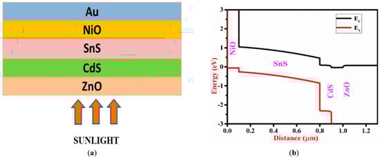
Figure 1.
(a) Schematic structure and (b) energy band diagram of the proposed solar cell.

Table 1.
Parameters of ZnO [26], CdS [27], SnS [28] and NiO [14] used in the simulation of proposed solar cell.
Table 2.
Interface parameters used in the simulation of the proposed solar cell.
4. Results and Discussion
The heterostructure ZnO/CdS/SnS solar cells have VOC, JSC, FF and PCE of 0.4732 V, 33.739 mA/cm2, 71.79% and 11.46%, respectively. Figure 2a,b display the J-V characteristics and quantum efficiency (QE) of the heterostructure ZnO/CdS/SnS/NiO/Au solar cell. The improved solar cell achieved VOC, JSC, FF and PCE of 0.9048 V, 34.209 mA/cm2, 86.97% and 26.92%, respectively. After including NiO and other materials, the QE of the solar cell increases from the wavelength of 600-900 nm as shown in Figure 2(b). This enhancement of QE shows the reduction in surface carrier recombination at SnS that demonstrated the improvement of PCE after employing NiO as the HTL. The PCE of the enhanced cell is increased below the wavelength of 400 nm.
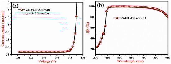
Figure 2.
(a) J-V curve and (b) quantum efficiency of the proposed heterojunction solar cell.
4.1. Impact of Carrier Concentration and Thickness of NiO and ZnO
The cell performance was studied in terms of carrier concentration and layer thickness. The thickness of NiO and ZnO was varied from 100 to 12,000 nm and carrier concentration was varied from 1014 to 1021 cm−3. The VOC is nearly independent of both carrier concentration and NiO thickness. The JSC varies significantly depending on carrier concentration and thickness. At a NiO carrier concentration of 1018 cm−3 and thickness of 250 nm, the optimal JSC of 34.20 mA/cm2 was obtained. The FF and PCE increase with an increase in carrier concentration but remain almost constant with increasing thickness. The series resistance decreases as the carrier concentration increases due to which FF and PCE rise [10]. At a NiO carrier concentration of 1021 cm−3 and thickness of 250 nm, the maximum PCE of 26.92% is recorded.
The thickness of ZnO does not have any effect on VOC but fluctuates with carrier concentration and achieves its maximum value of 0.9048 V at 1017 cm−3. The JSC worked similarly to the VOC and gave an optimal value of JSC 34.20 mA/cm2 at 1017 cm−3 carrier concentration. The increase in ZnO carrier concentration induced band bending resulting in a small rise in JSC. The FF had a reducing nature with increasing thickness of ZnO up to 1017 cm−3 because of increasing series resistance. Maximum efficiency of 26.92% is recorded at carrier concentration and thickness of 1017 cm−3 and 100 nm, respectively.
4.2. Impact of SnS/CdS Interface Defect Density
The influences of SnS/CdS interface defect density (IDD) on the performance of the proposed solar cell have been analysed. The SnS/CdS defect interface can increase the series resistance and carrier trapping of the cell. Due to the increase in carrier recombination rate at the interface, VOC decreases with IDD but IDD has no impact on JSC until 1017 cm2. JSC increases from 19.48 to 28.25 mA/cm2 when the width of SnS layer increases from 200 to 1200 nm. When IDD increases from 1011 to 1018 cm2, FF decreases rapidly from 84.9% to 54.8% due to an increase in the series resistance of the cell, indicating that high defect density at SnS/CdS is responsible for high series resistance. A significant decrease in PCE was also seen with increasing IDD. An interface defect is one of the reasons for lower PCE. Defects in the interfacial layer density are induced in the cell as a result of structural changes in the materials produced during the fabrication process.
4.3. Impact of Defect Density and Thickness of Absorber Layer SnS
The influence of absorber layer defect density and thickness is depicted in Figure 3 and Figure 4, respectively. The defect is caused by displacement and surface defects. Defects serve in carrier recombination, reducing mobility and carrier lifetime. The Shockley–Read–Hall (SRH) process modulates the recombination rate of SnS at higher defect density.
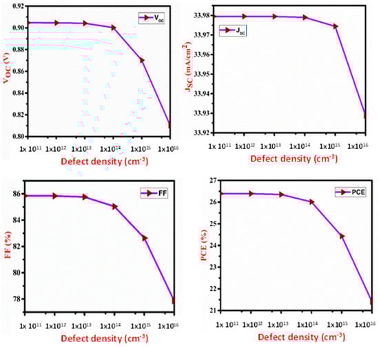
Figure 3.
Impact of defect density of SnS layer on VOC, JSC, FF and PCE of the proposed cell.
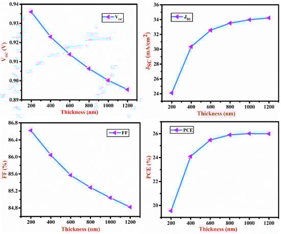
Figure 4.
Impact of SnS layer thickness on VOC, JSC, FF and PCE of the proposed cell.
The absorber layer thickness and defect density varied from 100 to 1200 nm and from 1011 to 1016 cm−3, respectively. VOC decreases with an increase in thickness and defect density of SnS but there is no effect of defect density on JSC below 1015 cm−3 due to an increase in carrier recombination. Due to the high absorption of increased wavelength photons in the layer, JSC increases up to a certain level with an increase in the thickness of SnS. After that, it saturates due to light absorption saturation. PCE is increased with SnS thickness as the JSC increases and saturates at 1200 nm due to the light absorption saturation. The fill factor shows the same nature as VOC. JSC, VOC and FF are all associated with PCE. At defect density of 1011 cm−3 and thickness of the SnS layer of 1000 nm, the maximum PCE of 26.92% is recorded.
4.4. Impact of Electron Affinity and Back Contact Metal Work Function of Absorber Layer SnS
Figure 5 depicts the effect of SnS electron affinity (EA). The maximum performance of the cell was obtained at SnS EA of 4.3 eV. Due to a decrease in FF, PCE falls with EA > 4.3 eV due to a mismatch of energy level between the SnS and CdS layer for electron transport as shown in Figure 5. VOC does not show any significant change with affinity due to insufficient carriers. The effect of back contact metal work function (WF) is shown in Figure 6. As the WF increases, JSC, VOC, FF and PCE also increase up to a certain WF level. This indicates that when WF rises, the majority carrier barrier height reduces. As a result, PCE rises with WF till 5 eV, and after 5 eV, PCE saturates. Thus, WF has a significant influence on the performance of the solar cell. Proper metal contact is necessary to achieve high efficiency. Table 3 shows a comparison of the physical parameters of various simulated device structures. Our findings seem to have a satisfying consistency with those that have already been published.
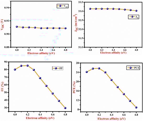
Figure 5.
Impact of the electron affinity of SnS layer on VOC, JSC, FF and PCE of the proposed cell.
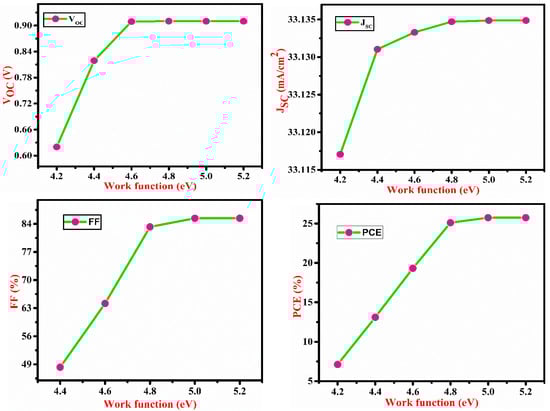
Figure 6.
Impact of back contact metal work function on VOC, JSC, FF and PCE of the proposed cell.
Table 3.
Comparison of previously reported results to proposed work.
5. Conclusions
The performance of the cell structure ZnO/CdS/SnS/NiO/Au has been investigated using SCAPS 1-D software. It is shown that NiO is a suitable HTL material with the ability to improve the efficiency of SnS-based solar cells. ZnO can be a good replacement for ITO and FTO in the fabrication of low-cost and highly efficient SnS-based solar cells. At ZnO and NiO carrier concentrations of 1017 and 1021 cm−3, respectively, and thicknesses of 100 and 250 nm, respectively, the maximum PCE of 26.92% is recorded. The thickness and defect density of the SnS layer were also investigated. As the SnS thickness increases, the PCE of the cell also increases. The maximum PCE of the proposed solar cell is recorded at thickness and defect density of 1000 nm and 1011 cm−3. The present work might give an insight into the modelling and development of the high performance of SnS-based solar cells.
Author Contributions
Conceptualization, A.U., P.T., S., P.L. and D.K.D.; methodology, A.U., P.T., S., P.L. and D.K.D.; software, A.U., P.T., S., V.S., P.L., D.K.D. and H.Q.; validation, A.U., P.T., S., V.S., P.L., D.K.D., H.Q., S.A., H.A. and S.B.; formal analysis, A.U., P.T., S., V.S., P.L., D.K.D., H.Q., S.A., H.A. and S.B.; resources, A.U. and D.K.D.; data curation, A.U., P.T., S., V.S., P.L., D.K.D., H.Q., S.A., H.A. and S.B.; writing—original draft preparation, A.U., P.T., S. and D.K.D.; writing—review and editing, A.U., S., D.K.D., H.Q., S.A. and S.B.; supervision, A.U., S. and D.K.D.; project administration, A.U. and D.K.D.; funding acquisition, A.U. All authors have read and agreed to the published version of the manuscript.
Funding
The authors are thankful to the Deanship of Scientific Research at Najran University, Najran, Kingdom of Saudi Arabia, for funding this work under the Research Group Funding Program grant NU/RG/SERC/11/1.
Data Availability Statement
All data is provided in the manuscript.
Acknowledgments
The authors are thankful to the Deanship of Scientific Research at Najran University, Najran, Kingdom of Saudi Arabia, for funding this work under the Research Group Funding Program grant NU/RG/SERC/11/1. The authors also thank Mark Burgelman for developing the SCAPS-1D software and making it freely accessible to the entire scientific community.
Conflicts of Interest
The authors declared no potential conflict of interest.
References
- Andrade-Arvizu, J.A.; Courel-Piedrahita, M.; Vigil-Galán, O. SnS-based thin film solar cells: Perspectives over the last 25 years. J. Mater. Sci. Mater. Electron. 2015, 26, 4541–4556. [Google Scholar] [CrossRef]
- Hammond, G.P.; Pearson, P.J. Challenges of the transition to a low carbon, more electric future: From here to 2050. Energy Policy 2013, 52, 1–9. [Google Scholar] [CrossRef]
- Huang, J.; Xiang, S.; Yu, J.; Li, C.-Z. Highly efficient prismatic perovskite solar cells. Energy Environ. Sci. 2018, 12, 929–937. [Google Scholar] [CrossRef]
- Wang, C.; Liu, M.; Rahman, S.; Pasanen, H.P.; Tian, J.; Li, J.; Deng, Z.; Zhang, H.; Vivo, P. Hydrogen bonding drives the self-assembling of carbazole-based hole-transport material for enhanced efficiency and stability of perovskite solar cells. Nano Energy 2022, 101, 107604. [Google Scholar] [CrossRef]
- Li, R.; Liu, M.; Matta, S.K.; Hiltunen, A.; Deng, Z.; Wang, C.; Dai, Z.; Russo, S.P.; Vivo, P.; Zhang, H. Sulfonated Dopant-Free Hole-Transport Material Promotes Interfacial Charge Transfer Dynamics for Highly Stable Perovskite Solar Cells. Adv. Sustain. Syst. 2021, 5, 2100244. [Google Scholar] [CrossRef]
- Patel, M.; Mukhopadhyay, I.; Ray, A. Molar optimization of spray pyrolyzed SnS thin films for photoelectrochemical applications. J. Alloys Compd. 2015, 619, 458–463. [Google Scholar] [CrossRef]
- Tumen-Ulzii, G.; Matsushima, T.; Adachi, C. Mini-Review on Efficiency and Stability of Perovskite Solar Cells with Spiro-OMeTAD Hole Transport Layer: Recent Progress and Perspectives. Energy Fuels 2021, 35, 18915–18927. [Google Scholar] [CrossRef]
- Devika, M.; Reddy, N.K.; Ramesh, K.; Patolsky, F.; Gunasekhar, K. Weak rectifying behaviour of p-SnS/n-ITO heterojunctions. Solid-State Electron. 2009, 53, 630–634. [Google Scholar] [CrossRef]
- Jeganath, K.; Choudhari, N.J.; Pai, G.S.; Rao, A.; Raviprakash, Y. Role of substrate temperature on spray pyrolysed metastable π-SnS thin films. Mater. Sci. Semicond. Process. 2020, 113, 105050. [Google Scholar] [CrossRef]
- Yang, R.; Wang, D.; Jeng, M.; Ho, K.; Wang, D. Stable CdTe thin fi lm solar cells with a MoO x back- contact buffer layer. Prog. Photovolt. Res. Appl. 2016, 24, 59–65. [Google Scholar] [CrossRef]
- Irfan, I.; Lin, H.; Xia, W.; Wu, H.N.; Tang, C.W.; Gao, Y. The effect of MoOx inter-layer on thin film CdTe/CdS solar cell. Sol. Energy Mater. Sol. Cells 2012, 105, 86–89. [Google Scholar] [CrossRef]
- Lin, H.; Irfan, H.; Xia, W.; Wu, H.N.; Gao, Y.; Tang, C.W. MoOx back contact for CdS/CdTe thin film solar cells: Preparation, device characteristics, and stability. Sol. Energy Mater. Sol. Cells 2012, 99, 349–355. [Google Scholar] [CrossRef]
- Shen, K.; Yang, R.; Wang, D.; Jeng, M.; Chaudhary, S.; Ho, K.; Wang, D. Stable CdTe solar cell with V2O5 as a back contact buffer layer. Sol. Energy Mater. Sol. Cells 2016, 144, 500–508. [Google Scholar] [CrossRef]
- Ahmmed, S.; Aktar, A.; Hossain, J.; Ismail, A.B.M. Enhancing the open circuit voltage of the SnS based heterojunction solar cell using NiO HTL. Sol. Energy 2020, 207, 693–702. [Google Scholar] [CrossRef]
- Kazemzadeh, M.; Ranjbar, M.; Kermanpur, A.; Taghaviniaet, N.; Minbashi, M.; Forouzandeh, M.; Ebadi, F. Enhanced performance of planar perovskite solar cells using TiO2/SnO2 and TiO2/WO3 bilayer structures: Roles of the interfacial layers. Sol. Energy 2020, 208, 697–707. [Google Scholar]
- Agrawal, S.; Rane, R.; Mukherjee, S. ZnO Thin Film Deposition for TCO Application in Solar Cell. Conf. Pap. Energy 2013, 2013, 718692. [Google Scholar] [CrossRef]
- Muchuweni, E.; Sathiaraj, T.; Nyakotyo, H. Synthesis and characterization of zinc oxide thin films for optoelectronic applications. Heliyon 2017, 3, e00285. [Google Scholar] [CrossRef]
- Wang, K.-C.; Jeng, J.-Y.; Shen, P.-S.; Chang, Y.-C.; Diau, E.W.-G.; Tsai, C.-H.; Chao, T.-Y.; Hsu, H.-C.; Lin, P.-Y.; Chen, P.; et al. p-type Mesoscopic Nickel Oxide/Organometallic Perovskite Heterojunction Solar Cells. Sci. Rep. 2014, 4, 4756. [Google Scholar] [CrossRef]
- Reese, M.O.; Barnes, T.M.; Jensen, S.A.; Metzger, W.K. The Roles of Carrier Concentration and Interface, Bulk, and Grain-Boundary Recombination for 25% Efficient CdTe Solar Cells. J. Appl. Phys. 2017, 121, 214506. [Google Scholar]
- Nayak, P.K.; Mahesh, S.; Snaith, H.J.; Cahen, D. Photovoltaic solar cell technologies: Analysing the state of the art. Nat. Rev. Mater. 2019, 4, 269–285. [Google Scholar] [CrossRef]
- Kavitha, N.; Chandramohan, R.; Valanarasu, S.; Vijayan, T.A.; Rosario, S.R.; Kathalingam, A. Effect of film thickness on the solar cell performance of CBD grown CdS/PbS heterostructure. J. Mater. Sci. Mater. Electron. 2015, 27, 2574–2580. [Google Scholar] [CrossRef]
- Alam Moon, M.; Ali, H.; Rahman, F.; Hossain, J.; Ismail, A.B. Design and Simulation of FeSi2-Based Novel Heterojunction Solar Cells for Harnessing Visible and Near-Infrared Light. Phys. Status solidi 2020, 217, 1900921. [Google Scholar] [CrossRef]
- Et-Taya, L.; Ouslimane, T.; Benami, A. Numerical analysis of earth-abundant Cu2ZnSn(SxSe1-x)4 solar cells based on Spectroscopic Ellipsometry results by using SCAPS-1D. Sol. Energy 2020, 201, 827–835. [Google Scholar] [CrossRef]
- Procel, P.; Xu, H.; Saez, A.; Ruiz-Tobon, C.; Mazzarella, L.; Zhao, Y.; Han, C.; Yang, G.; Zeman, M.; Isabella, O. The role of heterointerfaces and subgap energy states on transport mechanisms in silicon heterojunction solar cells. Prog. Photovolt. Res. Appl. 2020, 28, 935–945. [Google Scholar] [CrossRef]
- Benabbasa, S.; Rouabaha, Z.; Bouarissab, N.; Chelalia, N. The role of back surface field SnS layer in improvement of efficiency of CdTe thin film solar cells. Optik 2016, 127, 6210–6217. [Google Scholar] [CrossRef]
- Boudour, S.; Bouchama, I.; Hadjab, M.; Laidoudi, S. Optimization of defected ZnO/Si/Cu2O heterostructure solar cell. Opt. Mater. 2019, 98, 109433. [Google Scholar] [CrossRef]
- Nykyruy, L.; Yavorskyi, R.; Zapukhlyak, Z.; Wisz, G.; Potera, P. Evaluation of CdS/CdTe thin film solar cells: SCAPS thickness simulation and analysis of optical properties. Opt. Mater. 2019, 92, 319–329. [Google Scholar] [CrossRef]
- Tiwari, P.; Alotaibi, M.F.; Al-Hadeethi, Y.; Srivastava, V.; Arkook, B.; Sadanand, S.; Lohia, P.; Dwivedi, D.K.; Umar, A.; Algadi, H.; et al. Design and Simulation of Efficient SnS-Based Solar Cell Using Spiro-OMeTAD as Hole Transport Layer. Nanomaterials 2022, 12, 2506. [Google Scholar] [CrossRef]
- Kutwade, V.V.; Gattu, K.P.; Sonawane, M.E.; Tonpe, D.A.; Mishra, M.K.; Sharma, R. Contribution in PCE enhancement: Numerical designing and optimization of SnS thin film solar cell. J. Nanopart. Res. 2021, 23, 146. [Google Scholar] [CrossRef]
- Boubakri, A.; Jouidri, A.; Koumya, Y.; Rajira, A.; Almaggoussi, A.; Abounadi, A. An output characteristics simulation of SnS based solar cells. Mater. Today Proc. 2021, 51, 2047–2052. [Google Scholar] [CrossRef]
Publisher’s Note: MDPI stays neutral with regard to jurisdictional claims in published maps and institutional affiliations. |
© 2022 by the authors. Licensee MDPI, Basel, Switzerland. This article is an open access article distributed under the terms and conditions of the Creative Commons Attribution (CC BY) license (https://creativecommons.org/licenses/by/4.0/).