Abstract
An inverted ridge 3D thermal optical (TO) switch of a graphene-coated polymer/silica hybrid waveguide is proposed. The side electrode structure is designed to reduce the mode loss induced by the graphene film and by heating the electrode. The graphene layer is designed to be located on the waveguide to assist in the conduction of heat produced by the electrode. The inverted ridge core is fabricated by etching and spin-coating processes, which can realize the flat surface waveguide. This core improves the transfer of the graphene layer and the compatibility of the fabrication processes. Because of the opposite thermal optical coefficient of polymer and silica and the high thermal conductivity of the graphene layer, the 3D hybrid TO switch with low power consumption and fast response time is obtained. Compared with the traditional TO switch without graphene film, the power consumption of the proposed TO switch is reduced by 41.43% at the wavelength of 1550 nm, width of the core layer (a) of 3 μm, and electrode distance (d) of 4 μm. The rise and fall times of the proposed TO switch are simulated to be 64.5 μs and 175 μs with a d of 4 μm, and a of 2 μm, respectively.
1. Introduction
Three-dimensional (3D) hybrid integrated chips have the advantages of a high integration degree of photonic chips, improvement and diversification in device function, and low signal crosstalk; consequently, these chips can be applied to optoelectronic integration fields and 3D integration fields [1,2]. A variety of optical devices such as vertical amplifiers [3,4], optical waveguides [5,6], optical switches [7,8], lasers [9,10], and optical detectors [11,12] can be integrated on a single chip according to their respective functions. The hybrid integration of different material systems is the key factor in optical devices. However, integrating different materials has the problems of refractive index mismatch, large coupling loss, and poor material compatibility. Up to now, matched materials are mainly focused on silica, glass, and polymer in 3D integration optical devices [13,14].
A key goal of 3D hybrid integrated optical devices is to realize the optical path switching between different layers. Therefore, the X-junction vertical structure optical switch has been proposed [15,16,17]. In 2018, Qian Qian Song fabricated an X-junction thermo-optic with a silicon oxynitride (SiON) core and polymer cladding, realizing a power consumption of 59.6 mW and rise and fall times of 1.42 ms and 0.85 ms, respectively [18]. Among the structures of X-junction optical switches, the organic–inorganic hybrid X-junction optical switch can realize the lower power consumption because of the different thermal optical (TO) coefficients of the polymer and inorganic material. In contrast, the organic–inorganic hybrid Mach Zehnder interferometer (MZI) optical switch can realize lower power consumption than the X-junction optical switch [19]. In 2012, a polymer/silica hybrid MZI thermo-optic switch was fabricated with a power consumption lower than 7.2 mW and rise and fall times of 106 μs and 93 μs, respectively [20]. However, it was a planar thermal optical (TO) switch.
To further reduce the power consumption of the vertical optical devices, the polymer/silica hybrid MZI TO switches with a graphene film have attracted attention. Two-dimensional graphene material has many excellent optical properties such as large thermal conductivity, high carrier mobility, and wide optical response spectrum [21]. Therefore, graphene-based TO devices can realize lower power consumption and fast response time [22,23,24]. However, this device based on graphene material generally has a large optical loss due to the optical absorption of graphene material, and the fabrication process of graphene-based 3D MZI TO devices is limited. The first reason is that the uneven surface of the waveguide destructs the graphene film and affects the performance of the switch. Moreover, the structure of multilayer integration leads to alignment problems of the template after spin-coating a new layer that is not conducive to the matching between different layers of the waveguide. To solve these problems, the inverted ridge waveguide structure can be applied, realizing the flat surface waveguide, helping transfer the graphene layer. The structure of the inverted ridge waveguide can be realized by an etching process [25,26] or imprinting processes [27] such as hot imprinting [28] and nanoimprinting [29]. Because the etching process is beneficial to realize the compatibility of silica and polymer materials, the polymer/silica hybrid device with fast response time can be realized. Moreover, for the devices with loss compensation, the silica grooves structure fabricated by the etching process can avoid the solubility of core layer and cladding materials due to the benzene in the solvent. Finally, the etching process also has the advantages of high etching precision and low loss.
In this paper, a 2 × 2 MZI-inverted ridge TO switch of a graphene–polymer–silica hybrid waveguide with side electrode structure is proposed. The waveguide grooves are designed to be fabricated by the etching process. Then, the polymer core layer was obtained by polymer spin-coating in grooves. This process can realize the compatibility of silica and polymer materials and the flat surface waveguide, thus helping in the transfer of the graphene film. Because of the high thermal conductivity of the graphene layer and the opposite thermal optical coefficient of polymer and silica, the 3D-inverted ridge TO switch of the graphene–polymer–silica hybrid waveguide with low power consumption and fast response time can be obtained.
2. Device Design and Theoretical Analysis
The 3D structure of the MZI-inverted ridge 3D hybrid TO switch with a graphene film is shown in Figure 1a. Figure 1b,c show the cross-sectional structure in the heating region and the 3-dB coupling regions, respectively. The device consists of a silica core layer, silica cladding, polymer inverted ridge core layer, gold electrode, graphene layer, and silicon under substrate. Because of the large thermal conductivity of the graphene material coated on the polymer core layer, it helps conduct the heat generated by the electrode in the polymer waveguide, increasing the change of the effective refractive index due to the increase in the temperature in the polymer core layer.
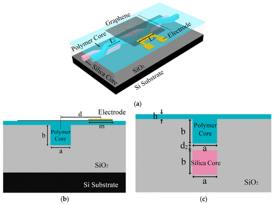
Figure 1.
(a) Three-dimensional structure; (b) two-dimensional cross-sectional structure in the heating region (the position of the red dotted line in Figure 1a); and (c) two-dimensional cross-sectional structure in the 3-dB coupling regions (the position of the black dotted line in Figure 1a) of the inverted ridge 3D hybrid thermal optical (TO) switch with graphene film and side electrode structure.
The dimensions of the core layers are a = b = 3 μm. The parameters of m = 6 μm, Le = 1 cm, and d2 = 0.6 μm indicate the width of the electrode, length of the electrode, and coupling gap between two waveguide core layers, respectively. The thickness of the slab layer is h = 1.22 μm. The coupling length of the waveguide in the vertical direction is Lc. The horizontal distance between the center of the core layer and the center of the electrode is d. nc1 = 1.48, nc2 = 1.478, and n1 = 1.444 are the refractive indices of the silica core layer, polymer core layer, and silica cladding layer, respectively. When the effective refractive index of the two core layers is equal, the optical field can be theoretically fully coupled in a 3-dB coupler. When heating the electrode, the effective refractive index of the waveguide changed, realizing the phase change of π.
The thermo-optical coefficients of the polymer and silica are −2.36 × 10⁻⁴/°C and 1.28 × 10⁻⁵/°C. The phase change ∆Φ can be expressed as:
where the ∆Nneff is the effective refractive index change, and λ is the wavelength of waveguide (set at 1550 nm). Because of the large thermal conductivity of a graphene layer (thermal conductivity of graphene layer kg = 5300 W/mK, thermal conductivity of polymer kp = 0.19 W/mK), the graphene layer is coated on the waveguide to assist the conduction of heat produced by the electrode. This process helps realize the phase shift at a lower power consumption (P) of the 3D hybrid TO switch.
The optical field distribution and the thermal field distribution of the devices are simulated by finite element analysis software. The simulation processes include geometry build, add material, physics analysis, meshing build, study, and results analysis. For the optical field analysis, the physics interfaces are “electromagnetic waves” and “frequency domain”. The meshing method and the study method are “physics-controlled mesh” and “mode analysis”, respectively. For the thermal field analysis, the physics interface is “heat transfer in solids”. The meshing method and the study method are “free triangular mesh” and “stationary”, respectively. First, the top electrode structure of the TO switch by lithography process has been simulated (as shown in Figure 2). n2 is the refractive index of the polymer cladding layer. To realize the complete coupling of light field, the structure of the waveguide has been optimized (a = b = 3 μm; the height of cladding hcladding = 6 μm; nc1 = 1.48; nc2 = 1.478; n1 = 1.444; n2 = 1.451). Figure 2a,b show the 3D structure and the cross-sectional structure in the heating region, respectively, for the TO switch with top electrode structure. Figure 2c,d show the light field distribution and thermal field distribution of the TO switch, respectively. The power consumption of the TO switch with top electrode structure is 4.2 mW when the temperature change is 1.6 K. Second, the inverted ridge 3D hybrid TO switches with side electrode structure are simulated in Figure 3 (a = b = 3 μm; nc1 = 1.48; nc2 = 1.478; n1 =1.444; h =1.22 μm; d = 4 μm). Figure 3a,b show the light field distribution and thermal field distribution of the inverted ridge TO switch without a graphene film. The temperature change is 2.74 K, and the power consumption is 7.02 mW. Figure 3c,d show the light field distribution and thermal field distribution of the inverted ridge TO switch with a graphene-assisted heating layer. The temperature change is 0.96 K, and the power consumption is 2.46 mW. Because of the large thermal conductivity of the graphene layer, the heat produced by the electrode conducts along the graphene film, increasing the temperature of the waveguide (as shown in Figure 3b,d). Because the top electrode structure requires a polymer cladding to reduce the device losses, and the 2D graphene layer helps the heat conduct in a transverse direction for the side electrode structure. Compared with the TO switch with a top electrode structure, the power consumption of the graphene-based inverted ridge TO switch with side electrode structure is reduced by 41.43% (as shown in Figure 2d and Figure 3d).
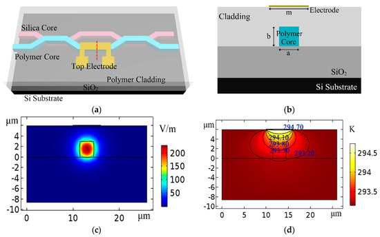
Figure 2.
TO switch with top electrode structure by a lithography process. (a) Three-dimensional structure; (b) two-dimensional cross-sectional structure in the heating region (the position of the red dotted line in Figure 2a); (c) optical field distribution in the heating region; (d) thermal field distribution in the heating region.
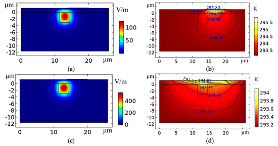
Figure 3.
Inverted ridge TO switch with side electrode structure. (a) Optical field distribution in the heating region without a graphene film; (b) thermal field distribution in the heating region without a graphene film; (c) optical field distribution in the heating region for a graphene TO switch; (d) thermal field distribution in the heating region for a graphene TO switch.
The light field coupling for the inverted ridge TO switch was simulated by 3D BeamPROP module of the Rsoft software. The light outputs from polymer core were launched from the silica core with an a of 3 μm, h of 1.22 μm, Lc of 2.049 mm, m of 6 μm, Le of 1 cm, nc1 of 1.48, nc2 of 1.478, and n1 of 1.444. The 3D geometric model of the TO switch constructed with Rsoft software is shown in Figure 4a. The light transmission in x–y direction of the TO switch at z axis positions of 440 μm, 2784 μm, 3676 μm, 12,180 μm, 24,104 μm, 25,476 μm, 28,260 μm is shown in Figure 4b–h, respectively. Figure 5 shows the simulated light field coupling between silica waveguide and polymer waveguide in x–z direction. It shows that the coupling in the vertical direction can be realized in the MZI TO switch. The calculated coupling efficiency is 97.5%.
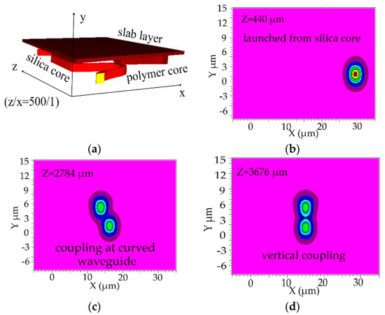
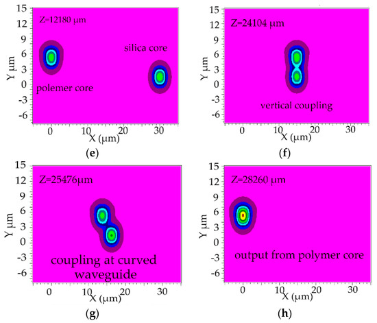
Figure 4.
(a) The 3D geometric model of the inverted ridge TO switch; (b–h) corresponding to the light transmission in x–y direction at z axis positions of 440 μm, 2784 μm, 3676 μm, 12,180 μm, 24,104 μm, 25,476 μm, 28,260 μm, respectively (a = 3 μm, h = 1.22 μm; Lc = 2.049 mm; m = 6 μm, L = 1 cm, nc1 = 1.48, nc2 = 1.478 and n1 = 1.444).
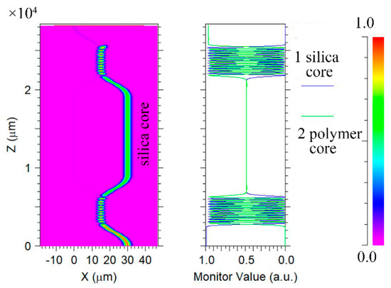
Figure 5.
Simulated light field coupling is launched from silica core for the inverted TO switch with a graphene film and side electrode structure.
3. Optimization and Discussions
The modal losses of the graphene TO switch are related to the graphene film, position of the gold electrode, and dimension of the waveguide. The refractive indexes of the gold electrode and graphene film are 0.559 + 11.5i and 2.973 + 2.79i, respectively [16]. The calculation of the mode losses is dependent on the imaginary part of the effective refractive index of the waveguide, which can be expressed as [30,31]:
Figure 6 shows the calculated mode losses (α) induced by graphene film and electrode as a function of horizontal distances (d) between the center of the core layer and the electrode with the electrode width (a) from 1.5 to 3.5 μm. Five different polymer core layer dimensions are designed by COMSOL, realizing the complete coupling between two waveguide core layers. Because of the absorption of light by the side electrode, as shown in Figure 6, the mode losses are significantly reduced (less than 1.5 dB/cm) and insensitive to the width of the core layer for the side electrode structure (d > 4 μm).
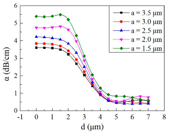
Figure 6.
Calculated mode losses induced by graphene film and electrode with different horizontal distances between the center of the core layer and the electrode (a1 = 3.5 μm, h1 = 1.24 μm; a2 = 3 μm, h2 = 1.22 μm; a3 = 2.5 μm, h3 = 1.20 μm; a4 = 2 μm, h4 = 1.18 μm; a5 = 1.5 μm, h5 = 1.14 μm; m = 6 μm, L = 1 cm, nc1 = 1.48, nc2 = 1.478 and n1 = 1.444).
Figure 7 shows the calculated power consumption using finite element analysis software as a function of the horizontal distance between the center of the core layer and the electrode for a = 3 μm and a = 2 μm, respectively. For the TO switch without a graphene film structure, the power consumption significantly increases as a function of electrode distance (d). The power consumption is 3.2 mW with a d of 0 μm, while the power consumption increases to 17.26 mW with a d of 7 μm. For the graphene TO switch structure, the power consumption is insensitive to the electrode distance because of the large thermal conductivity of graphene film, relaxing the tolerances during the fabrication work of the devices. The results show that the power consumption for the graphene TO switch with d of 4 μm is reduced by 23.13% compared with the top electrode TO switch structure (d = 0 μm) without graphene film.
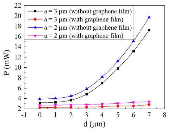
Figure 7.
Calculated power consumption as a function of the horizontal distance between the center of the core layer and the electrode for a = 3 μm and a = 2 μm, respectively.
The calculated response time and the power consumption with different electrode widths (d = 4 μm) are shown in Figure 8. Figure 8 shows that by reducing the width of the core layer from 4.5 to 1.5 μm, the rise time was shortened from 75.8 to 55.1 μs, the fall time was shortened from 188.2 to 174 μs, and the power consumption was increased from 2.36 mW to 3.59 mW. It indicated that the small size of the core layer can achieve a fast response time. The large size of the core layer can realize low power consumption due to the small temperature change when phase change of π was realized.
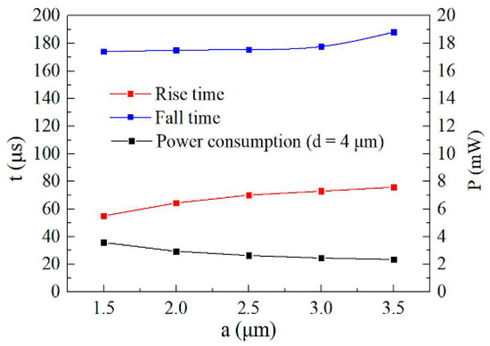
Figure 8.
Calculated response time and the power consumption as a function of the electrode width (d = 4 μm).
Figure 9 shows the response time curves of the side electrode TO switch with a graphene heating layer, which is simulated by finite element analysis software. The study method is “time dependent”, and a square wave with upper limit of 0.0007 is added in the TO switch. The rise and fall times were 64.5 μs and 175 μs with a d of 4 μm, a of 2 μm, ∆T of 1.15 K, and P of 2.95 mW, respectively.
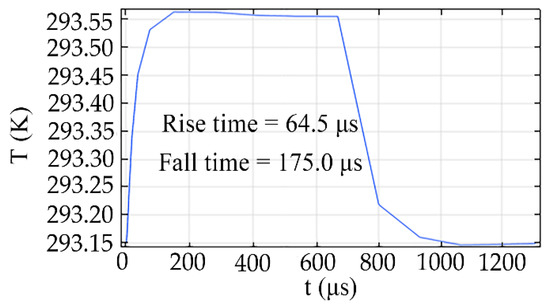
Figure 9.
The response time curves of the graphene TO switch with a d of 4 μm and a of 2 μm.
4. Conclusions
In summary, we have presented an inverted ridge 3D hybrid TO switch with graphene film. Because of the opposite thermal optical coefficients of polymer and silica and the high thermal conductivity of a graphene layer, a graphene-based side electrode TO switch with low power consumption and fast response time has been obtained. Compared with the traditional 3D polymer–silica hybrid TO switch with top electrode structure, the power consumption was reduced by 41.43% for the graphene TO switch with a d of 4 μm, a of 3 μm, electrode length of 1 cm, and wavelength of 1550 nm. Compared with the inverted ridge TO switch with a top electrode structure, the power consumption was reduced by 23.13% for the graphene TO switch with a d of 4 μm. Moreover, the rise and fall times were 64.5 μs and 175 with a d of 4 μm, a of 2 μm, ∆T of 1.15 K, and P of 2.95 mW, respectively.
Author Contributions
Conceptualization, D.Z. and Y.Y. (Yunji Yi); software, Y.C.; validation, D.Z., Y.Y. (Yunji Yi), and F.W.; Formal analysis, Y.C.; Data curation, Y.C. and Y.Y. (Yue Yang); Methodology, Y.C. and B.L.; Funding acquisition, D.Z. and Y.Y. (Yunji Yi); Project administration, D.Z.; Resources, J.L., H.Z. and B.L.; Writing—original draft, Y.Y. (Yunji Yi) and Y.C.; Writing—review and editing, F.W. and Y.Y. (Yunji Yi). All authors have read and agreed to the published version of the manuscript.
Funding
This work was supported by the National Key Research and Development Program of China (2019YFB2203001) and Science and Technology Development Plan of Jilin Province (20190302010GX).
Conflicts of Interest
The authors declare no conflict of interest.
References
- Song, J.; Luo, X. Three-dimensional (3D) monolithically integrated photodetector and WDM receiver based on bulk silicon wafer. Opt. Express 2014, 22, 19546–19554. [Google Scholar] [CrossRef] [PubMed]
- Stone, A.; Jain, H. Direct laser-writing of ferroelectric single-crystal waveguide architectures in glass for 3D integrated optics. Sci. Rep. 2015, 5, 10391. [Google Scholar] [CrossRef] [PubMed]
- Forget, S.; Balembois, F. A new 3D multipass amplifier based on Nd:YAG or Nd:YVO4 crystals. Appl. Phys. B Lasers Opt. 2002, 75, 481–485. [Google Scholar] [CrossRef][Green Version]
- Hurtado, A.; Henning, I.D. Bistability and nonlinear gain in 1.55 μ m vertical cavity semiconductor optical amplifiers: Theory and experiments. Appl. Phys. Lett. 2007, 91, 151106. [Google Scholar] [CrossRef]
- Woods, R.; Feldbacher, S. 3D optical waveguides produced by two photon photopolymerisation of a flexible silanol terminated polysiloxane containing acrylate functional groups. Opt. Mater. Express 2014, 4, 486–498. [Google Scholar] [CrossRef]
- Han, X.; Zhang, Z.; Yang, J.; Xiao, H.; Ren, G.; Jiang, Y.; Zhao, T.; Nguyen, T.; Mitchell, A.; Yang, J.; et al. On-chip switchable and reconfigurable optical mode exchange device using cascaded three-waveguide-coupling switches. Opt. Express 2020, 28, 9552–9562. [Google Scholar] [CrossRef]
- Ohkoshi, S.; Takano, S. 90-degree optical switching of output second-harmonic light in chiral photomagnet. Nat. Photonics 2014, 8, 65–71. [Google Scholar]
- Vlasov, Y.; Green, W.M.J.; Xia, F. High-throughput silicon nanophotonic wavelength-insensitive switch for on-chip optical networks. Nat. Photonics 2008, 2, 242–246. [Google Scholar] [CrossRef]
- Popa, D.; Sun, Z. Graphene Q-switched, tunable fiber laser. Appl. Phys. Lett. 2011, 98, 073106. [Google Scholar] [CrossRef]
- Lancaster, D.G.; Gross, S.; Ebendorff-Heidepriem, H.; Withford, M.J.; Monro, T.M.; Jackson, S.D. Efficient 29 μm fluorozirconate glass waveguide chip laser. Opt. Lett. 2013, 38, 2588–2591. [Google Scholar] [CrossRef]
- Hadfield, R.H. Single-photon detectors for optical quantum information applications. Nat. Photonics 2009, 3, 696–705. [Google Scholar] [CrossRef]
- Han, Z.; Singh, V.; Kita, D.; Monmeyran, C.; Becla, P.; Su, P.; Li, J.; Huang, X.; Kimerling, L.C.; Hu, J.; et al. On-chip chalcogenide glass waveguide-integrated mid-infrared PbTe detectors. Appl. Phys. Lett. 2016, 109, 071111. [Google Scholar] [CrossRef]
- Qiu, C.; Wang, Y. Design and Analysis of a Novel Graphene-Assisted Silica/Polymer Hybrid Waveguide with Thermal-Optical Phase Modulation Structure. IEEE Photonics J. 2019, 11, 1–10. [Google Scholar] [CrossRef]
- Bian, Y.; Zheng, Z.; Zhao, X.; Zhu, J.; Zhou, T. Symmetric hybrid surface plasmon polariton waveguides for 3D photonic integration. Opt. Express 2009, 17, 21320–21325. [Google Scholar] [CrossRef]
- Pandit, M.K.; Chan, H.P. The WDM performance of compact X-junction switches in polymer. Microw. Opt. Technol. Lett. 2001, 28, 423–426. [Google Scholar]
- Chan, H.P.; Chow, C.K. A wide-angle X-junction polymeric thermooptic digital switch with low crosstalk. IEEE Photonics Technol. Lett. 2003, 15, 1210–1212. [Google Scholar]
- Oh, M.; Lee, H. Asymmetric X-junction thermooptic switches based on fluorinated polymer waveguides. IEEE Photonics Technol. Lett. 1998, 10, 813–815. [Google Scholar]
- Song, Q.Q.; Chen, K.X. Low-power total internal reflection thermo-optic switch based on hybrid SiON-polymer X-junction waveguides. Appl. Opt. 2018, 57, 9809–9813. [Google Scholar] [PubMed]
- Xu, Q.; Jiang, M. Fast and low-power thermo-optic switch based on organic-inorganic hybrid strip-loaded waveguides. Opt. Lett. 2018, 43, 5102–5105. [Google Scholar]
- Yan, Y.; Zheng, C. Response-time improvement of a 2 × 2 thermo-optic switch with polymer/silica hybrid waveguide. Opt. Commun. 2012, 285, 3758–3762. [Google Scholar]
- Ansell, D.; Radko, I.P. Hybrid graphene plasmonic waveguide modulators. Nat. Commun. 2015, 6, 8846. [Google Scholar] [CrossRef] [PubMed]
- Sun, Y.; Cao, Y. A low-power consumption MZI thermal optical switch with a graphene-assisted heating layer and air trench. Rsc Adv. 2017, 7, 39922–39927. [Google Scholar] [CrossRef]
- Chang, Z.; Chiang, K.S. Ultra-broadband mode filters based on graphene-embedded waveguides. Opt. Lett. 2017, 42, 3868–3871. [Google Scholar] [CrossRef]
- Hao, T.; Chang, Z. Externally pumped low-loss graphene-based fiber Mach-Zehnder all-optical switches with mW switching powers. Opt. Express 2019, 27, 4216–4225. [Google Scholar] [CrossRef]
- Debnath, K.; Khokhar, A.Z. Low-Loss Slot Waveguides with Silicon (111) Surfaces Realized Using Anisotropic Wet Etching. Front. Mater. 2016, 3, 5. [Google Scholar] [CrossRef]
- Bazylenko, M.V.; Gross, M. Effect of reactive ion etching-generated sidewall roughness on propagation loss of buried-channel silica waveguides. Appl. Phys. Lett. 1996, 69, 2178–2180. [Google Scholar] [CrossRef]
- Zhang, C.; Subbaraman, H. Printed photonic elements: Nanoimprinting and beyond. J. Mater. Chem. C 2016, 4, 5133–5153. [Google Scholar] [CrossRef]
- Wan, L.; Zhu, N. All-polymeric planar waveguide devices based on a gas-assisted thermal imprinting technique. Microsyst. Technol. 2017, 23, 5271–5279. [Google Scholar] [CrossRef]
- Hiltunen, M.; Heinonen, E. Nanoimprint Fabrication of Slot Waveguides. IEEE Photonics J. 2013, 5, 2200808. [Google Scholar] [CrossRef]
- Hida, Y.; Hida, Y. Polymer waveguide thermooptic switch with low electric power consumption at 1.3 μm. IEEE Photonics Technol. Lett. 1993, 5, 782–784. [Google Scholar] [CrossRef]
- Chang, Z.; Chiang, K.S. Experimental verification of optical models of graphene with multimode slab waveguides. Opt. Lett. 2016, 41, 2129–2132. [Google Scholar] [CrossRef] [PubMed]
© 2020 by the authors. Licensee MDPI, Basel, Switzerland. This article is an open access article distributed under the terms and conditions of the Creative Commons Attribution (CC BY) license (http://creativecommons.org/licenses/by/4.0/).