Abstract
The waveguide chip with a phase measurement function has garnered significant attention in the field of imaging optics, emerging as a crucial component in optical interferometric imaging systems. Enhancing the working bandwidth of these waveguide chips is essential for improving the imaging quality of interferometric systems. However, most existing designs primarily focus on narrow bands, with no reported research on broadband designs. This paper introduces a novel broadband waveguide chip design that incorporates a phase measurement function. We explore the fundamental structure and working principle of this innovative design. Fabricated on a silicon substrate, the chip features a silicon dioxide cladding layer and a germanium-doped silicon dioxide core layer, strategically optimized for performance. Utilizing the Beam Propagation Method (BPM), we conduct detailed simulations to determine the optimal device parameters. The simulation results demonstrate the effectiveness of our design, showing a phase measurement deviation of approximately 5° at a center wavelength of 1550 nm across a 300 nm wavelength range. The loss of the device is approximately 0.8 dB. These findings provide a solid foundation for future experimental implementations and fabrications, offering both a theoretical framework and technical reference for advancing the practical use of broadband waveguide chips with phase measurement functions in optical interferometric imaging.
1. Introduction
The waveguide chip with a phase difference measurement is a crucial component in the field of imaging optics [1]. Utilizing integrated optical technology, it has several advantages, including compact size, stable output phase, and low manufacturing cost [2]. It measures the phase difference between the two input light beams by analyzing the magnitude of the light intensity, and has a wide range of applications in various fields, such as coherent optical communication [3,4], optical imaging [5,6], optical sensing [7], etc. This paper focuses on its application requirements in the field of optical interferometric imaging. In particular, it addresses the requirements for broadband phase measurement chips used in photonic integrated interferometric imaging systems, such as the Segmented Planar Imaging Detector for Electro-Optical Reconnaissance (SPIDER) and checkerboard imager [8], which are based on the Van Cittert–Zernike Theorem [9]. The imaging system utilizes waveguide chips with a phase measurement function to measure the mutual coherence factor related to the target to be observed and then reconstructs a clear image through an inverse Fourier transform [10]. The mutual coherence factor can be expressed as , where is the modulus and is the phase. It is essential to ensure the imaging quality of the image by keeping the deviation between the measured phase and the actual phase below 0.18π. That is, the phase measurement deviation is less than 32.4° [11]. The size of the SPIDER and CheckerBoard imager has been significantly reduced due to the use of integrated waveguide devices, making it easier to launch into space and reducing the cost of space transportation [12]. Its stable performance makes it suitable not only for deep space exploration but also for monitoring the Earth’s surface. Potential applications include early warning systems for floods in rivers and lakes, meteorological forecasting, and seismic disaster monitoring [13]. To ensure that the imaging system is adaptable to various operational scenarios, it is essential to maximize the measurement signal-to-noise ratio (SNR). Increasing the operational bandwidth is a direct and effective method to enhance SNR; however, expanding the bandwidth also tends to increase measurement errors, thereby reducing imaging quality. This paper focuses on optimizing the design parameters of the waveguide chip to increase bandwidth while ensuring the measurement accuracy required for acceptable imaging quality.
Waveguide chips with phase measurement functions can be categorized based on fabrication materials, including lithium niobate, indium phosphide, silicon, and silicon dioxide [14,15]. The earliest material commonly used for waveguide chips with phase measurement functions was lithium niobate. In 1989, D. Hoffmann et al. produced an 8-port waveguide chip with a lithium niobate substrate, achieving a phase difference of 90° ± 5° [16]. Indium phosphide-based chips, first designed and fabricated by E.C.M. Pennings et al. [13], commonly use the self-imaging effect in multimode waveguides, operating within 1530–1565 nm with a maximum phase deviation of 1.4° [17,18,19,20,21].
In 2010, Furukara developed a silica-based waveguide chip with a relative refractive index difference of 1.8%, reducing the device size to 12 mm × 12 mm and achieving a phase deviation of 90° ± 1° within 1530–1565 nm [22]. In 2011, R. Halir et al. created a silicon dioxide substrate and silicon etching layer chip, reducing the size to 0.65 mm × 0.53 mm with a phase deviation within ±5° in the 1510–1565 nm range [23]. In 2013, Wei Yang et al. designed an SOI-based chip with a length of 0.107 mm and a phase deviation within 5° in the 1540–1570 nm range [24].
According to the preceding information, the device operates primarily within the C-band, with a narrow wavelength range of 30 nm to 50 nm. Despite this, research on the design of broadband waveguide chips remains limited. Expanding the bandwidth of the device can significantly improve the SNR of the interferometric imaging system, thereby enhancing overall imaging quality. This is crucial for advancing integrated optical interferometric imaging technology. Therefore, developing a broadband waveguide chip with phase measurement functions and excellent performance is essential.
In this paper, a broadband waveguide chip with a phase measurement function is simulated and designed. Firstly, the fundamental structure and working principle of the device are introduced, and then the structural parameters of the device are proceeded. The performance of the device is simulated, and the simulation results show that the size of the device is about 12 mm × 2.5 mm. When the incident light bandwidth is 300 nm with a center wavelength of 1550 nm, the phase measurement deviation is less than 5°, and the loss of the device is approximately 0.8 dB.
2. Materials and Methods
2.1. Working Principle and Structure
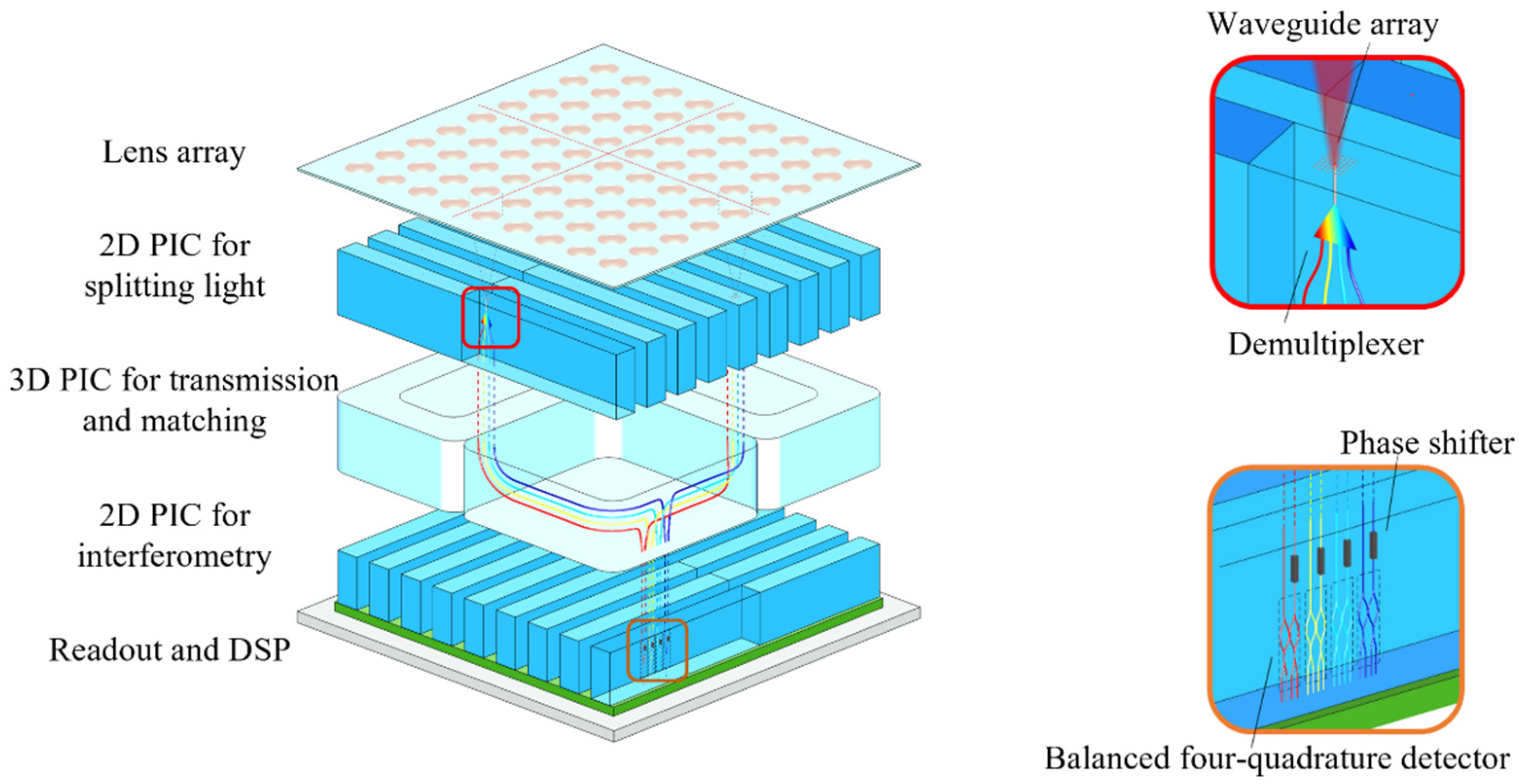
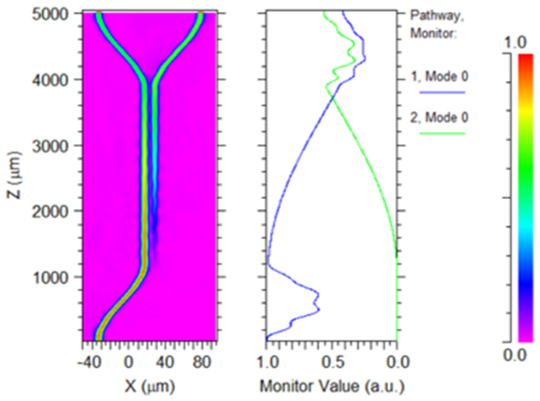
The “checkerboard” imager shown in Figure 1 is a classic structure of the photonics integrated interference imaging system [8]. The lens array of the “checkerboard” imager is set in a square grid arrangement, and three layers of PIC arrays are used. The first layer of 2D PIC after the lens array is used to acquire and split light from the target. The second layer of 3D PIC is used to transmit and match the light of each pair of lenses, bands, and sub-field. The third layer of 2D PIC is used for interferometry, where a balanced four quadrature detector is the waveguide chip with a phase measurement function, acquiring the mutual coherence factor of the target.

Figure 1.
The structure of the “checkerboard” imager.
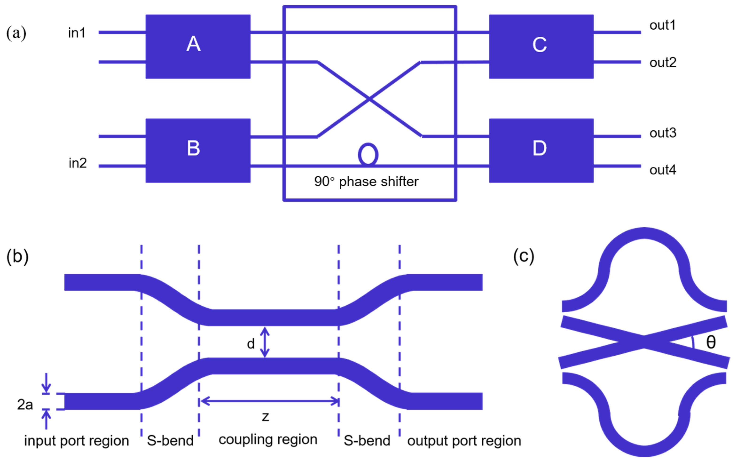
The schematic diagram of the balanced four quadrature detector with a wide bandwidth phase measurement function proposed is shown in Figure 2a. This device is mainly composed of a 90° phase shifter and 3 dB couplers labeled as A, B, C, and D. The schematic diagram of the 3 dB coupler is shown in Figure 2b, and Figure 2c is a schematic diagram of the connection section shown in the block diagram in Figure 2a. The role of the 90° phase shifter is to introduce a 90° phase difference in the optical path.
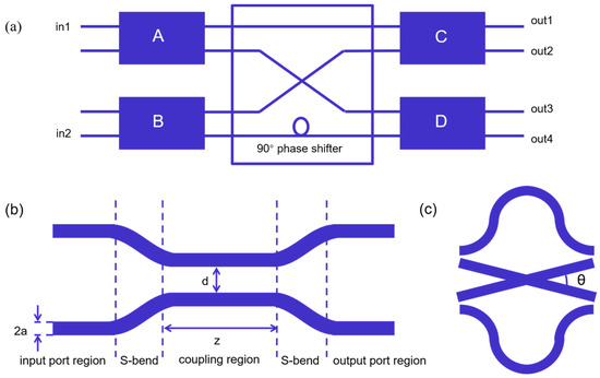
Figure 2.
(a) Schematic diagram of the waveguide chip with a phase measurement function; (b) Schematic diagram of a 3 dB coupler; (c) Schematic diagram of the connection section.
The amplitudes of the two input beams injected from input port in1 and input port in2 are and , respectively, and the phases are and , respectively. The input optical fields of the two input ports of the device can be expressed as follows:
The transmission matrix of the 3 dB coupler can be expressed as [25,26]:
In Equation (3), z is the coupling length, K is the coupling coefficient, and the expression for the coupling coefficient K is [27]:
In Equation (4), , , , , is the effective refractive index of the waveguide, is the waveguide radius, and is the waveguide spacing.
The two outputs of coupler A can be represented by the following matrix:
In Equation (5), is the output of the upper branch of coupler A, and is the output of the lower branch of coupler A.
Similarly, we can obtain the two outputs of coupler B:
In Equation (6), is the output of the upper branch of coupler B, and is the output of the lower branch of coupler B.
From Equations (5) and (6), we can obtain the inputs of coupler C and coupler D. The input matrices for coupler C and coupler D are given by Equation (7) and Equation (8), respectively.
In Equation (7), is the input of the upper branch of coupler C, and is the input of the lower branch of coupler C. In Equation (8), is the input of the upper branch of coupler D, and is the input of the lower branch of coupler D.
Therefore, we can obtain the output matrices of coupler C and coupler D as Equation (9) and Equation (10), respectively:
In Equation (9), is the output of the upper branch of coupler C, and is the output of the lower branch of coupler C. In Equation (10), is the output of the upper branch of coupler D, and is the output of the lower branch of coupler D.
Based on Equations (9) and (10), the light intensity values of the output beams of the four output ports of the device can be expressed as follows:
For monochromatic light, if the 3 dB coupler has a splitting ratio of 0.5, from Equations (11) to (14), the relationship between the phase difference and the light intensities , , , at the four output ports can be expressed as:
For broadband light, the dispersion effect of the device causes a deviation between the calculated phase difference using Equation (15) and the true value. To minimize phase measurement error while increasing bandwidth, it is necessary to carefully select the design parameters of the device.
2.2. Selection of Materials
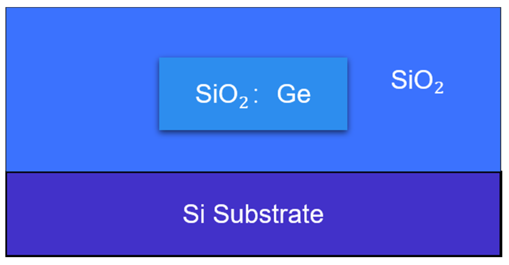
At present, there are various types of materials used in the production of optical waveguides, including silicon [28], silicon dioxide [29,30], lithium niobate [16], triple-five compounds such as indium phosphide [18], and polymers [31,32]. Each material offers distinct advantages and disadvantages. The choice of material depends on the specific functional requirements of the device to achieve optimal performance. Table 1 summarizes the characteristics of these materials. From Table 1, silica material has several advantages, such as minimal output phase deviation, a well-established fabrication process, low dispersion and lower cost [33,34]. Additionally, it is suitable for a broad bandwidth range [35]. Therefore, this paper selects silica-based optical waveguides for a series of simulations and optimizations. Figure 3 illustrates the cross-section of the optical waveguide made from silicon dioxide. The chosen three-dimensional structure is a widely used buried optical waveguide in waveguide-type optical devices. It consists of a silicon substrate with a silicon dioxide cladding layer (refractive index 1.445) and a core layer made of germanium-doped silicon dioxide. The refractive index of the core layer, which can be adjusted by varying the germanium doping concentration, is set to 1.456 to match the mode field with a 1550 nm single-mode fiber. This results in a relative refractive index difference of approximately 0.75% between the core and cladding layers [36].

Table 1.
Summary of different material characteristics.
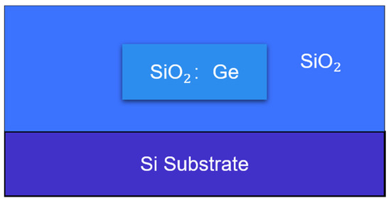
Figure 3.
Schematic of the cross-section of the optical waveguide made of silicon dioxide material.
2.3. Design of Waveguide Cross-Section Size
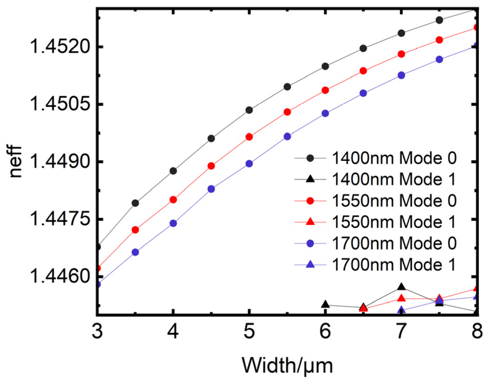
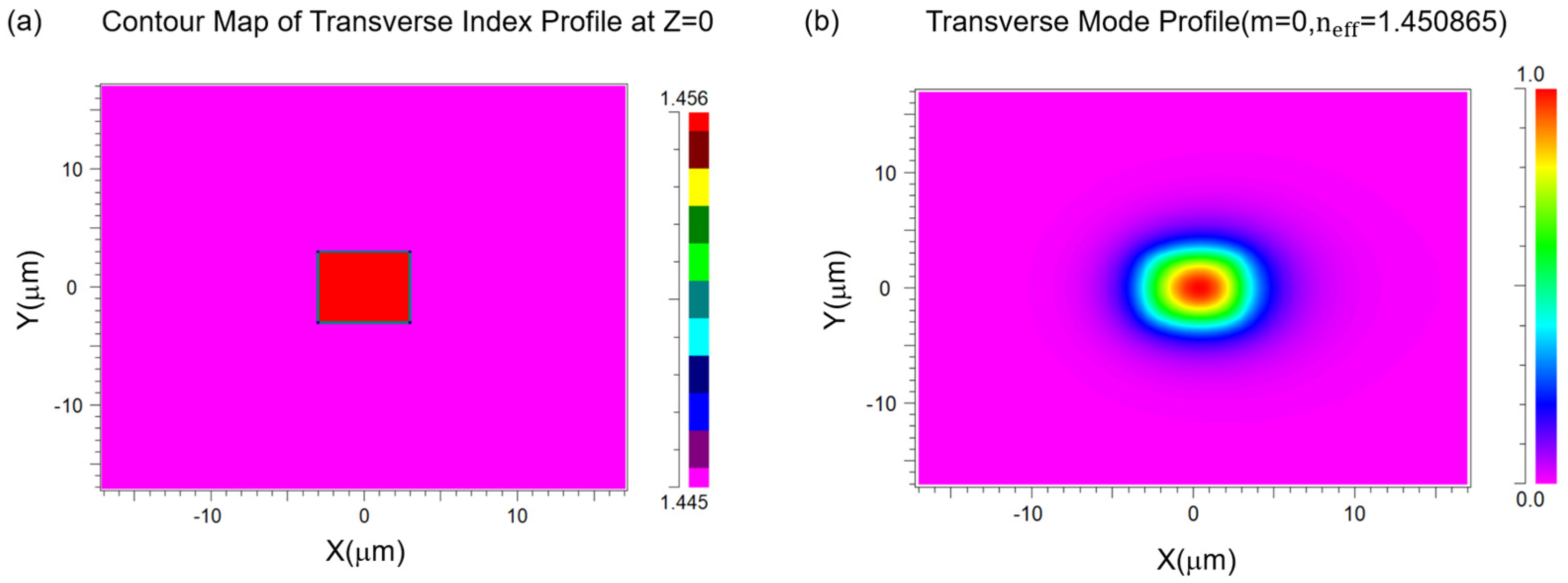
To achieve single-mode transmission, it is essential to carefully design the waveguide’s cross-sectional size, as single-mode transmission helps prevent mode dispersion and minimizes signal distortion. Based on the previous section, this paper adopts a center wavelength of 1550 nm, with silicon dioxide as the material. The refractive index of the cladding layer is 1.445, while the core layer has a refractive index of 1.456. Additionally, to reduce waveguide birefringence and transmission loss, this paper designs the waveguide with a square cross-section, where the width-to-height ratio is 1:1 [37]. Simulations are conducted to assess single-mode transmission for wavelengths of 1400 nm, 1550 nm, and 1700 nm. The results, shown in Figure 4, plot the waveguide width (in μm) on the horizontal axis and the effective refractive index on the vertical axis. The simulation results indicate that when the wavelength is 1400 nm, the first-order mode appears in the waveguide when the waveguide width reaches approximately 6 um. When the wavelength is 1550 nm, the first-order mode appears in the waveguide when the width reaches approximately 6.5 um. When the wavelength is 1700 nm, the first-order mode appears in the waveguide when the width reaches approximately 7 um. Therefore, to ensure single mode transmission in the wavelength range of 1400 nm to 1700 nm, the waveguide width should be approximately 6 µm or less. The simulations indicate that to ensure single-mode transmission within the wavelength range of 1400 nm to 1700 nm, the waveguide width should be approximately 6 μm or less. Since smaller waveguide dimensions increase fabrication complexity, a slightly larger cross-section is acceptable while still meeting single-mode requirements. Based on the simulation results and current fabrication capabilities, this paper selects a waveguide cross-section size of w = h = 6 μm. The schematic of the silicon dioxide rectangular optical waveguide model is depicted in Figure 5. The cross-sectional view of the silicon dioxide rectangular waveguide model is shown in Figure 5a, where the x-axis represents the width of the waveguide and the y-axis represents the height of the waveguide. The transverse mode field distribution of the straight waveguide is shown in Figure 5b, and the light field is well confined within the rectangular waveguide and the rectangular optical waveguide has = 1.450865.
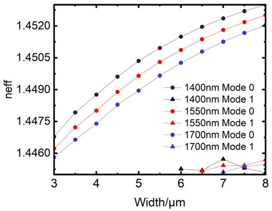
Figure 4.
Conditions of single mode transmission simulated waveguide at different wavelengths.
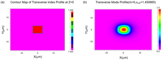
Figure 5.
Schematic diagram of the rectangular waveguide model in silicon dioxide (a) Cross-section of rectangular waveguide model; (b) Transverse mode field distribution of rectangular waveguide.
2.4. Design of 3 dB Coupler
The 3 dB coupler is a crucial component for forming a waveguide chip with a phase measurement function. Its schematic structure is illustrated in Figure 2b, and includes the input port region, the S-bend region, the coupling region, and the output port region. The beam splitting ratio is a vital parameter of the 3 dB coupler. The expression for the beam splitting ratio SR is [24]:
In Equation (16), is the coupling length, and is the coupling coefficient. From Equations (4) and (16), it can be observed that the parameters related to the beam splitting ratio are the wavelength , waveguide radius , waveguide spacing , coupling length, core refractive index , and cladding refractive index .
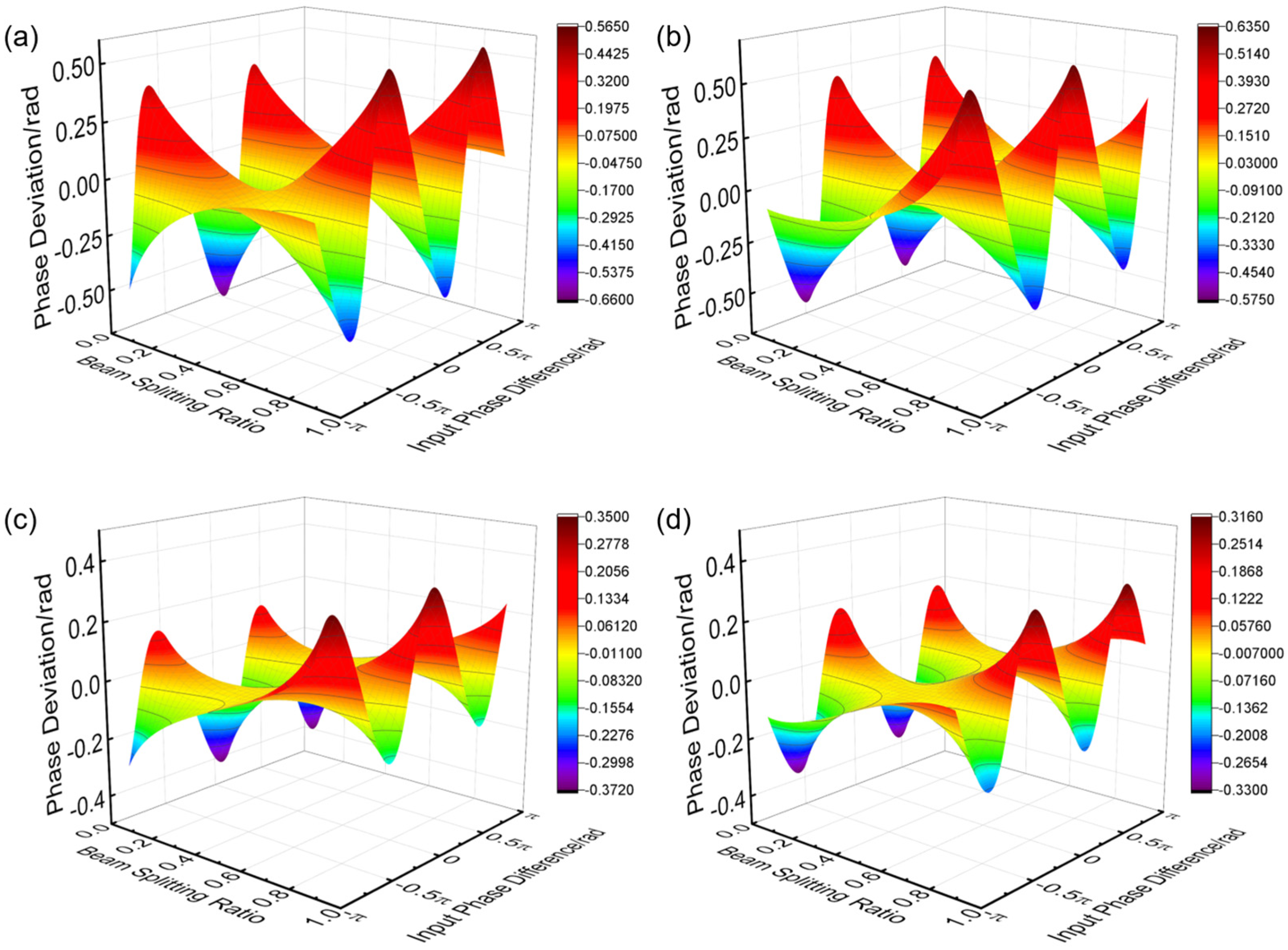
Assuming that the change of the input wavelength mainly leads to the change of the phase difference introduced by the delay line, but dose not only affects the beam splitting ratio of the 3 dB coupler. Based on Equations (4)–(10), the simulation results show the variation of phase deviation with input phase difference and input wavelength, as shown in Figure 6. When the beam splitting ratio of coupler A changes in the range of 0.1–0.9, the beam splitting ratio of coupler B, C, and D is set to 0.5, the input phase difference varies from −π to π, and the phase deviation varies in the range from −0.6570 rad to 0.5635 rad, as shown in Figure 6a. That is, the phase deviation is within 37.6°. When the beam splitting ratio of coupler B changes in the range of 0.1–0.9, the beam splitting ratio of coupler A, C, and D is set to 0.5, the input phase difference varies in the range of −π to π, and the phase deviation varies in the range from −0.5731 rad to 0.6329 rad, as shown in Figure 6b. That is, the phase deviation is within 36.3°. When the beam splitting ratio of coupler C changes in the range of 0.1–0.9, the beam splitting ratio of coupler A, B, and D is set to 0.5, the input phase difference varies in the range of −π to π, and the phase deviation varies in the range from −0.3718 rad to 0.3493 rad, as shown in Figure 6c. That is, the phase deviation is within 21.3°. When the beam splitting ratio of coupler D changes in the range of 0.1–0.9, the beam splitting ratio of coupler A, B, and C is set to 0.5, the input phase difference varies in the range of −π to π, and the phase deviation varies in the range from −0.3297 rad to 0.3145 rad, as shown in Figure 6d. That is, the phase deviation is within 18.9°. From the data above, it can be seen that the variation in beam splitting ratio of coupler A and coupler B has a more significant impact on the output of the chip than coupler C and coupler D. In addition, it also means that when the beam splitting ratio of each coupler changes in the range of 0.1–0.9, the phase measurement deviation basically meets the accuracy requirements of 0.18π (32.4°). This provides a rough range for our next step in the parameter design of the 3 dB coupler.
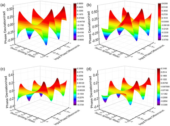
Figure 6.
Variation of phase deviation with the beam splitting ratio of a single coupler and input phase difference (a) the beam splitting ratio of coupler A changes; (b) the beam splitting ratio of coupler B changes; (c) the beam splitting ratio of coupler C changes; (d) the beam splitting ratio of coupler D changes.
The structural design of the 3 dB coupler mainly includes the parameter design of the input and output port region, the S-bend region, and the coupling region.
2.4.1. Design of the Waveguide Spacing in the Input and Output Port Region
For the 3 dB coupler, energy coupling occurs when the core layer spacing of the two input waveguides is too close. The same problem also exists in the core layer of the two output waveguides. To minimize non-essential energy coupling, it is essential to design a suitable waveguide spacing that avoids unintended coupling, thus reducing device loss and size. For a rectangular silica waveguide with a width and height of 6 μm, the relationship between the coupling length and the waveguide spacing is shown in Figure 7. In this figure, the horizontal axis represents the waveguide spacing, and the vertical axis represents the coupling length, with the unit in μm. From Figure 7, when the waveguide spacing is 20 μm, the waveguide coupling length reaches 4 m, and the coupling effect can be considered negligible. Therefore, this paper just needs to make sure that the spacing between the waveguide in the input and output port regions of the 3 dB coupler is designed to be greater than 20 μm.
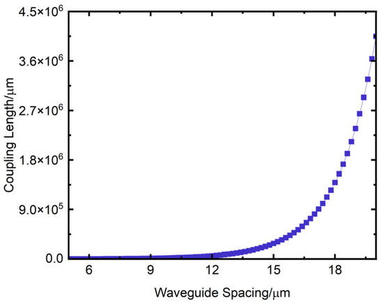
Figure 7.
Variation of coupling length with waveguide spacing.
2.4.2. Design of S-Bend Region Parameters
The S-bend region connects the input or output port regions with the coupling region. If the parameters of the S-bend region are not optimized, it can lead to significant transmission losses. Therefore, careful design and optimization of the S-bend parameters are crucial.
In this study, the cosine-type bending waveguide is employed due to its lower transmission loss compared to other designs [38]. The cosine-type bending waveguide structure is illustrated in Figure 8. The cosine-type bending waveguide has two important design parameters, namely the length L projected in the x-direction and the height h projected in the y-direction.
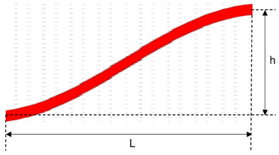
Figure 8.
Schematic of the cosine-type bending waveguide structure.
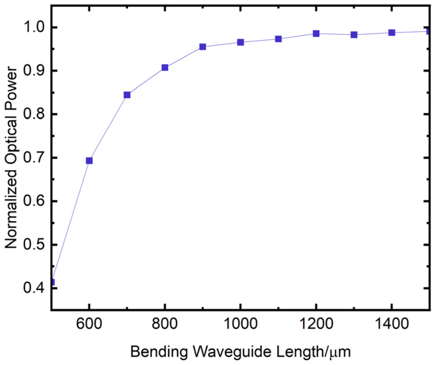
To balance device size reduction and prevent optical signal interference between adjacent paths, the value of h is usually set to 50 μm. When the center wavelength of the incident signal is λ = 1550 nm and the waveguide height is 50 μm, the relationship between the output power of the cosine-type bending waveguide and the bending waveguide length L is shown in Figure 9. The horizontal axis of the figure is the bending waveguide length L in μm. The vertical axis is the normalized output power of the waveguide. As observed, increasing the bending waveguide length L leads to a gradual increase in output power and a reduction in loss. However, once the bending waveguide length reaches 1000 μm or more, the loss levels off. From the curve in Figure 9, it can be seen that the normalized output power reaches its maximum value at 1200 μm, which means that the insertion loss is minimized at this point. Therefore, in this paper, the length of the bending waveguide is set to 1200 μm.

Figure 9.
Variation of the output power of cosine-type bending waveguide with bending waveguide length.
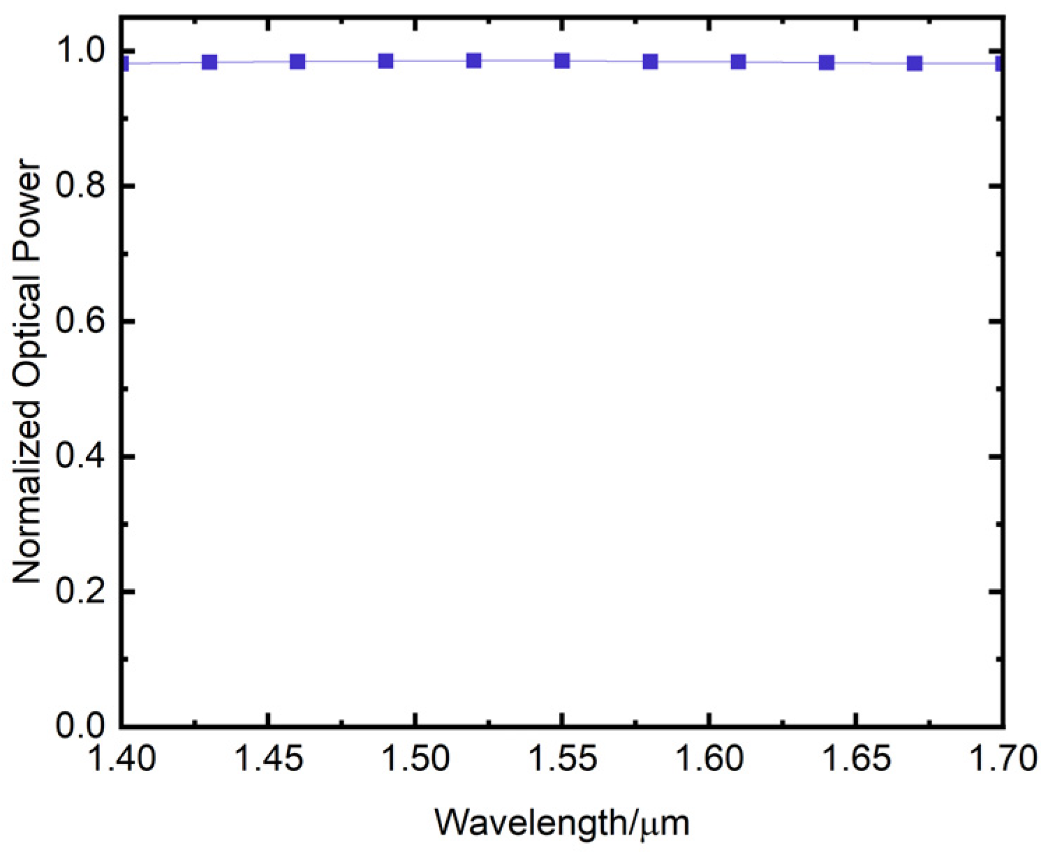
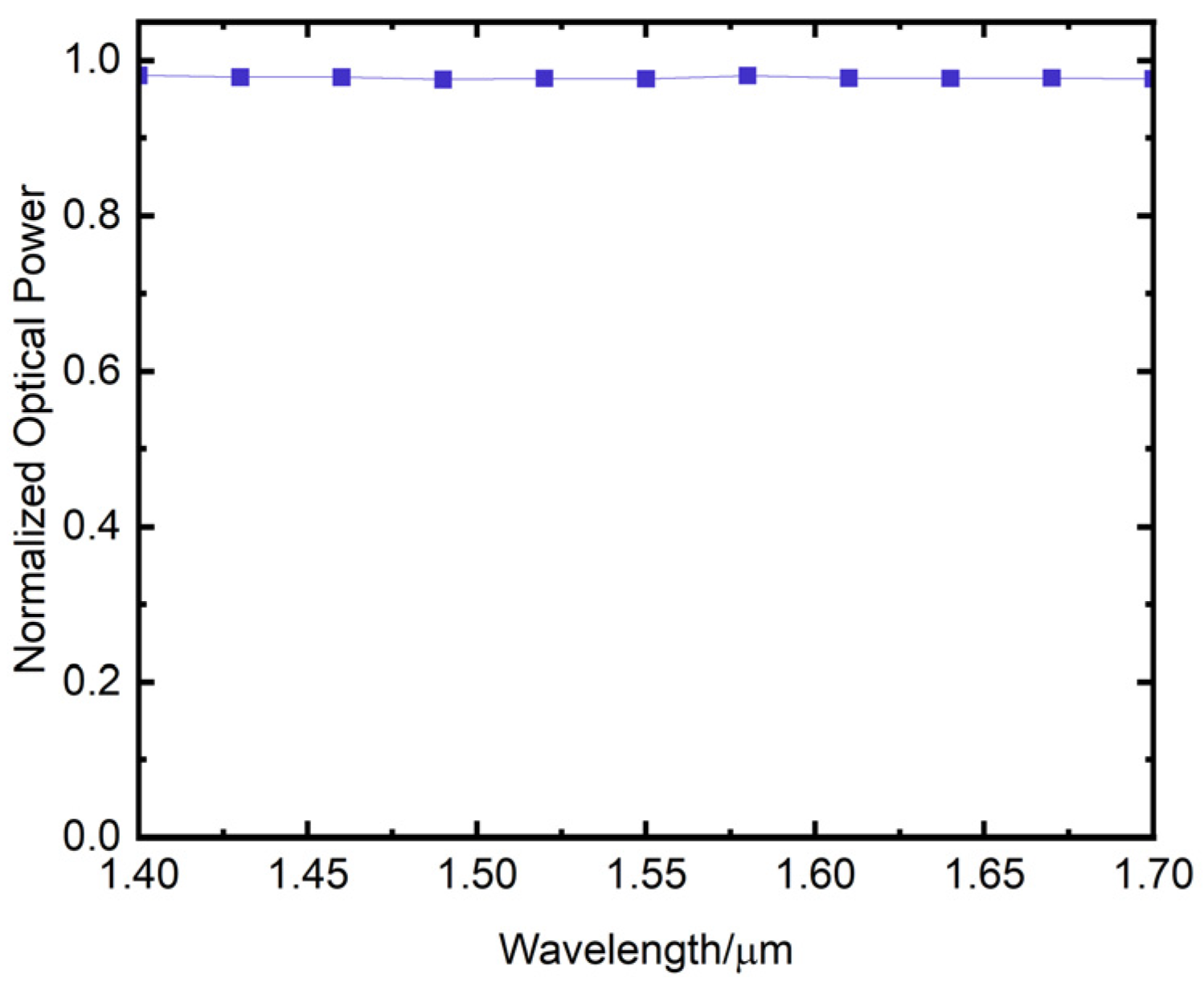
When the bending waveguide length is set to 1200 μm, Figure 10 illustrates the output power of the cosine-type bending waveguide as a function of the input wavelength. The horizontal axis represents the input wavelength in μm, while the vertical axis represents the normalized output power of the waveguide. The figure shows that the output power of the waveguide remains relatively constant within the input wavelength range of 1.4 μm–1.7 μm.

Figure 10.
Variation of the output power of cosine-type bending waveguide with input wavelength.
2.4.3. Design of Coupling Region Parameters
The structure of the coupling region, which is the core unit of the 3 dB coupler, is shown in Figure 11. The image shows two design parameters related to the coupling region, namely the waveguide spacing and the coupling length .
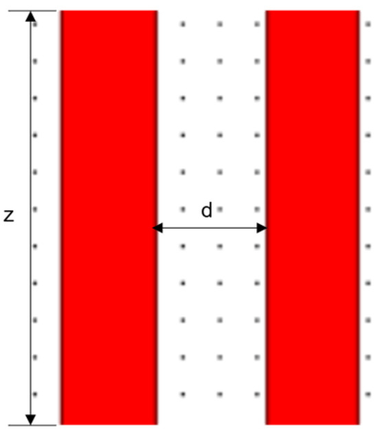
Figure 11.
Schematic diagram of the coupling region structure.
This paper first determines the waveguide spacing, which is mainly limited by the waveguide coupling. For the determined waveguide structure, the minimum coupling length of the 3 dB coupler increases exponentially as the waveguide spacing grows, and usually the value of the waveguide spacing is 6 μm~8 μm. Considering the goal of minimizing the size of the device, the waveguide spacing of the 3 dB coupler is designed as 6 μm in this paper. Then the value of the coupling length can be obtained. Based on the refractive index of the waveguide material and the waveguide cross-sectional dimensions, the coupling between the rectangular waveguides is simulated for an incident light with a center wavelength of λ = 1550 nm. The simulation structure is shown in Figure 11, and the results are shown in Figure 12. The left diagram in Figure 12 depicts the coupling transmission of the mode field, revealing that the mode field is gradually coupled to the right waveguide during the transmission process of the left waveguide. The mode coupling is accompanied by the optical energy also produces alternating coupling between the two waveguides as shown in the right diagram in Figure 12. It can be observed that when the coupling length reaches approximately 2600 μm (the intersection of the blue line and the green line in the right diagram of Figure 12), the output values of the two waveguides are equal, which means that the coupled waveguide can satisfy a splitting ratio of 1:1.
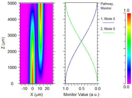
Figure 12.
Simulated simulation of rectangular inter-waveguide coupling.
Considering the influence of the bending waveguide on the coupling length, this paper simulates the transmission of optical signals with a wavelength of 1550 nm in the 3 dB coupler. Simulate the 3 dB coupler with the previously determined design parameters. Figure 13 shows the transmission results at an incident wavelength of 1550 nm. The output values of the two output ports are inconsistent (the values of the blue line and green line in the right diagram of Figure 13 when takes the maximum value), and have a significant difference which does not meet the design requirement of a 1:1 splitting ratio. This is because the equivalent coupling length generated by the bending waveguide in the S-bend region was not taken into consideration during the initial design process. Therefore, it is necessary to account for this factor to achieve the desired performance of the coupler.

Figure 13.
Optical signal transmission in a 3 dB coupler, when the coupling length of the 3 dB coupler is 2600 μm.
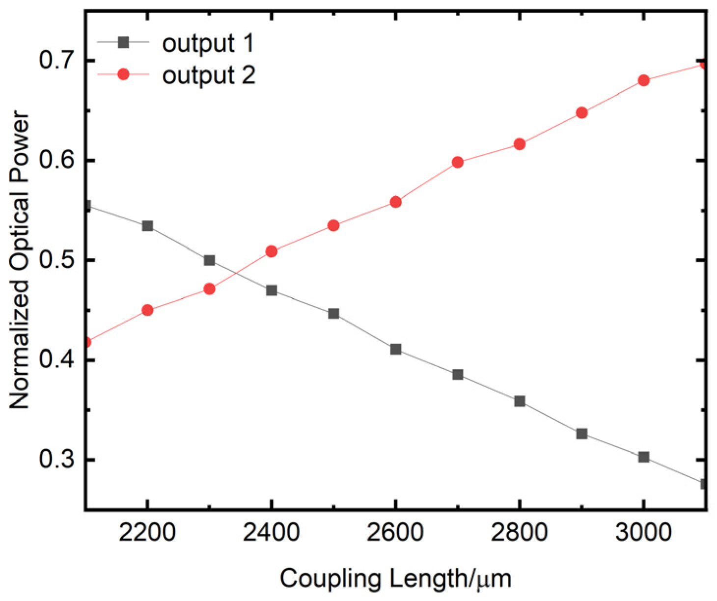
To further optimize the design parameters of the 3 dB coupler, a parameter scanning analysis of the coupling length is conducted. According to the previously determined design parameters of the bending waveguide, the variation of the two outputs (output1, output2) power of the 3 dB coupler with the coupling length is shown in Figure 14. The horizontal axis represents the coupling length in μm, while the vertical axis represents the normalized output power of the waveguide. From Figure 14, the straight waveguide length of the 3 dB coupler should be set to 2340 μm (the x-coordinate value of the intersection points between the black line and the red line in Figure 14).
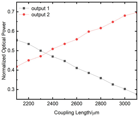
Figure 14.
Variation of the two outputs optical power of the 3 dB coupler with the coupling length.
Figure 15 presents the final transmission simulation results for the 3 dB coupler at a wavelength of 1550 nm with coupling length of 2340 μm. As can be seen from the right diagram of Figure 15, there is almost no difference between the output of the two output ports (the values of the blue line and green line in the right diagram of Figure 15 when takes the maximum value), meeting the design requirement of a 1:1 beam splitting ratio and achieving perfect beam splitting. As shown in Figure 15, when the input power is 1 unit, the single-branch output power of the 3 dB coupler is approximately 0.48. Therefore, the sum of the two outputs of the 3 dB coupler is 0.96, the insertion loss of the 3 dB coupler is about 0.18 dB.
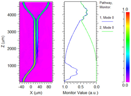
Figure 15.
Optical signal transmission in a 3 dB coupler, when the coupling length of the 3 dB coupler is 2340 μm.
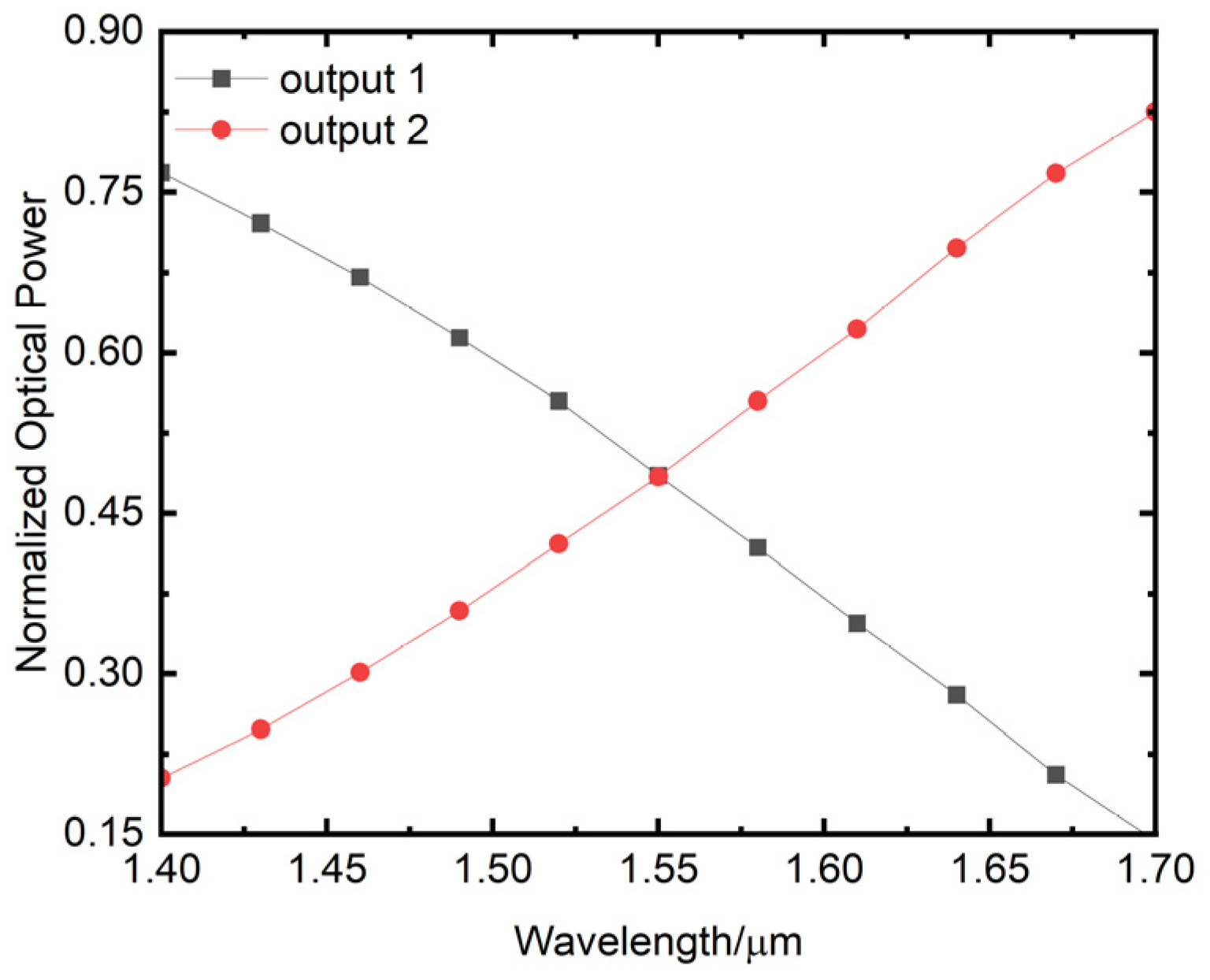
Based on the above determination of coupling length, numerical simulation analysis shows that when the input wavelength varies in the range of 1.4 μm–1.7 μm, the output of the 3 dB coupler (output1 and output2) varies between 0.14 and 0.83, as shown in Figure 16. The horizontal axis represents the wavelength in μm, while the vertical axis represents the normalized output power of the waveguide. The splitting ratio of the 3 dB coupler numerically equals the normalized output power at the two output ports. In other words, the splitting ratio of the 3 dB coupler varies between 0.14 and 0.83, which satisfies the requirement of beam splitting ratio of the 3 dB coupler for the design of the broadband phase measurement chip, with a measurement accuracy better than 0.18π.
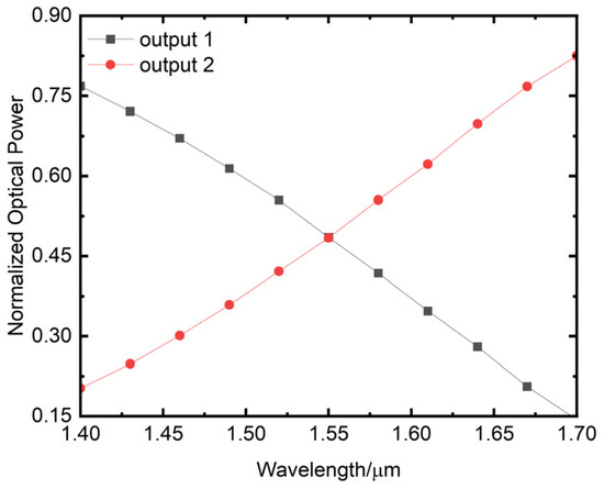
Figure 16.
Variation of the two outputs of the 3 dB coupler with wavelength.
2.5. Design of Bending Waveguide Parameter
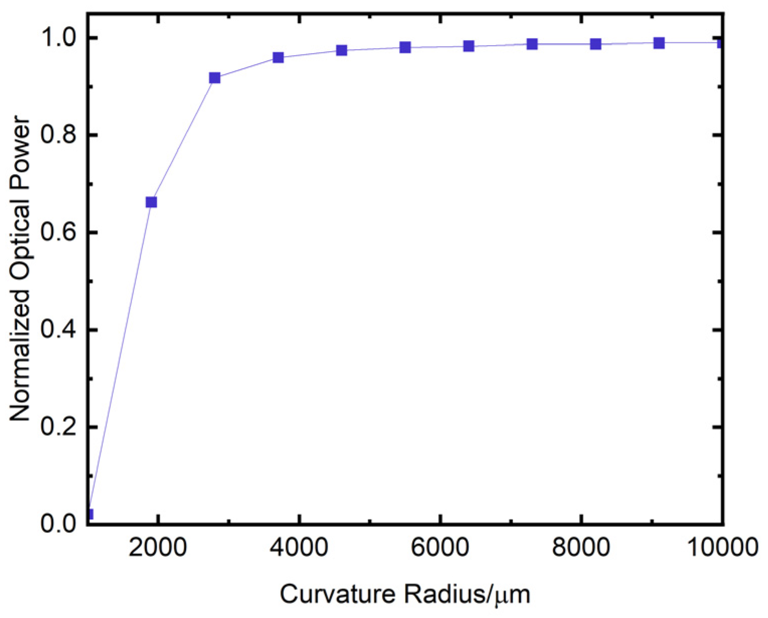
In addition to the bending waveguide in the S-bend region mentioned above, the connection section between the four 3 dB couplers also introduces the bending waveguide, as shown in Figure 2c. This bending waveguide may cause significant losses, so the design of the semicircular arc bending waveguide used at the turn of the device must be optimized. For the simulation of the semicircular arc bending waveguide, when the incident wavelength is 1550 nm, the length of the bending waveguide is 1500 μm and the values of the waveguide width and height are both 6 μm, the effect of different curvature radius on the output of the waveguide is shown in Figure 17. The horizontal axis of the figure is the waveguide curvature radius in μm, while the vertical axis is the output power of the waveguide. With the increase of the radius of curvature, the output power of the rectangular waveguide gradually increases. That is, the bending loss gradually decreases. From Figure 17, when the radius of the waveguide reaches more than 5000 μm, the loss tends to stabilize. The design of the bending waveguide focuses on reducing the insertion loss of the device and the device length. For the above reasons, this paper sets the curvature radius of the semicircular arc waveguide to 5000 μm. According to Figure 17, when the input power is 1 unit, the output power of the bending waveguide with a length of 1500 μm and a curvature radius of 5000 mm is approximately 0.98. From this, the loss of the bending waveguide can be calculated to be about 0.58 dB/cm.
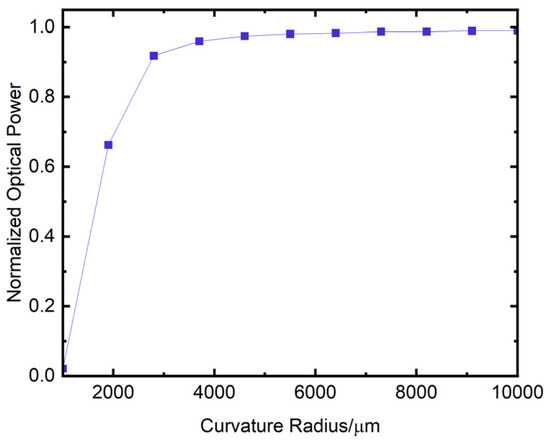
Figure 17.
Variation of the output power with curvature radius.
The variation in output power of the semicircular arc bending waveguide across an input wavelength range of 1.4 μm to 1.7 μm as shown in Figure 18. The horizontal axis of the figure is the wavelength in μm. The vertical axis is the output power of the waveguide. The figure shows that the output power of the waveguide remains relatively stable within the input wavelength range of 1.4 μm–1.7 μm.
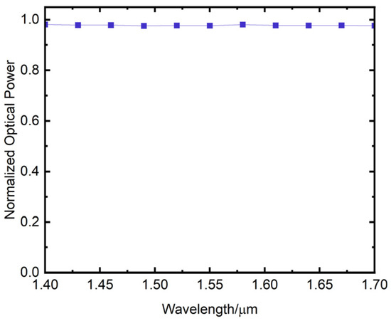
Figure 18.
Variation of the output power of a semicircular bending waveguide with input wavelength.
2.6. Design of Crossed Waveguide Parameter
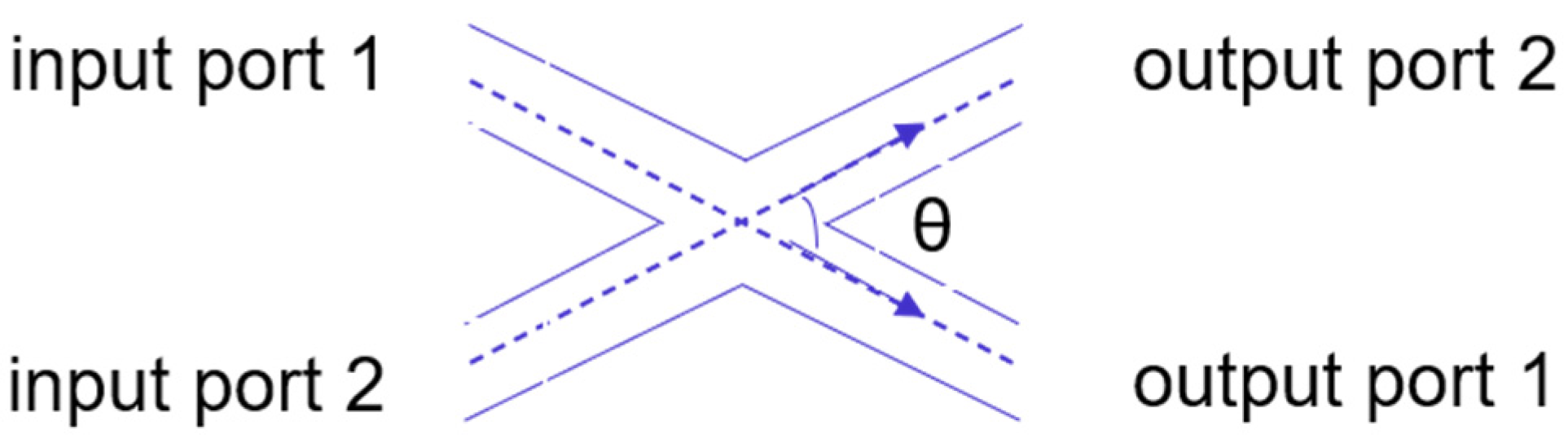
The 3 dB couplers labeled A and B, as well as the 3 dB couplers labeled C and D, involve a physical crossing of the waveguides during beam transmission. The structure of this configuration is illustrated in Figure 2c. Figure 19 shows the schematic structure of the crossed waveguide, with the crossing angle denoted as θ. The crossed waveguide introduces additional loss and crosstalk, therefore, the effect of the crossed waveguide on the performance of the device must be considered. To reduce the loss, the appropriate crossing angle must be selected. According to theory, the larger the crossing angle (right-angle crossing is optimal), the smaller the loss will be. However, the increase of the crossing angle will inevitably increase the size of the device, so it is necessary to carefully choose the appropriate crossing angle.
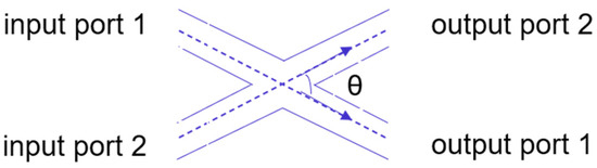
Figure 19.
Schematic diagram of crossed waveguide.
The loss of the crossed waveguide is simulated, with the layout of the crossed waveguides shown in Figure 20. In this setup, two optical waveguides intersect: one is vertical, and the other crosses it at an angle θ.
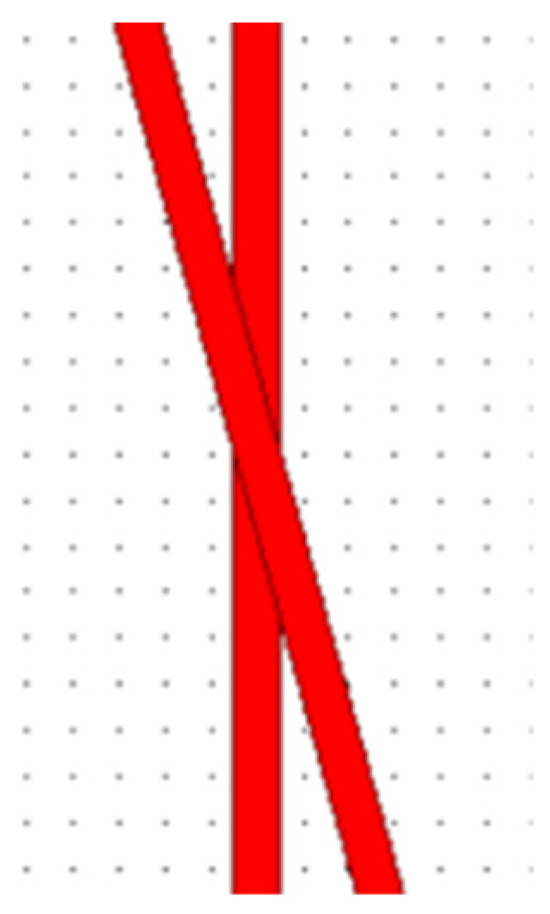
Figure 20.
Structure of the crossed waveguide.
Light with a wavelength of 1550 nm is incident from the vertical waveguide. As the crossing angle is varied, the change in optical power in the vertical waveguide is calculated, as depicted in Figure 21. In the figure, the horizontal axis represents the crossing angle in degrees, and the vertical axis represents the output power of the vertical waveguide. The figure shows that the output power of the vertical waveguide gradually increases with the increase of the crossing angle, and the output power changes slowly when the crossing angle reaches more than 30°. Therefore, the crossing angle selected in this paper is 30°. As shown in Figure 21, when the input power is 1 unit and the crossing angle is 30°, the output power of the vertical waveguide is approximately 0.98, from which the cross loss of the crossed waveguide can be calculated to be about 0.12 dB.
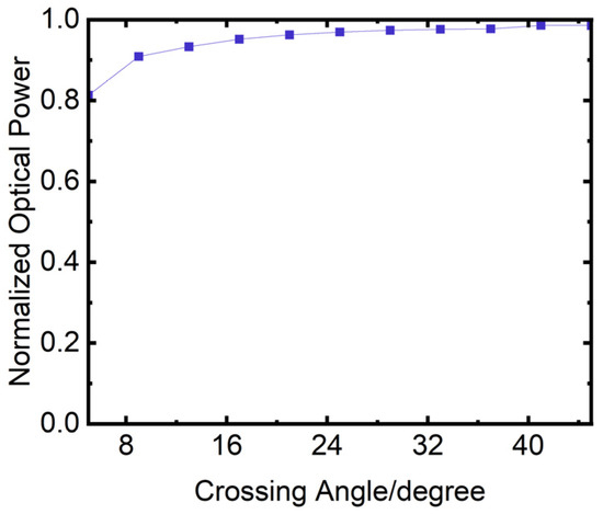
Figure 21.
Variation of vertical waveguide optical power with crossing angle.
When the crossing angle of the waveguide is set to 30°, the curve of the output power of the vertical waveguide changes with the input wavelength 1.4 μm–1.7 μm is shown in Figure 22. The horizontal axis of the figure is the input wavelength in μm and the vertical axis is the output power of the vertical waveguide. The figure shows that the output power of the waveguide remains relatively stable within the range of input wavelength from 1.4 μm to 1.7 μm.
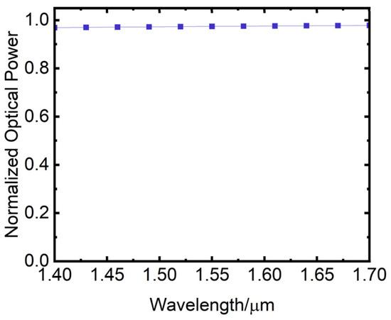
Figure 22.
Variation of output power at the vertical waveguide with input wavelength.
2.7. Design of 90° Phase Shifter and Connection Part Parameter
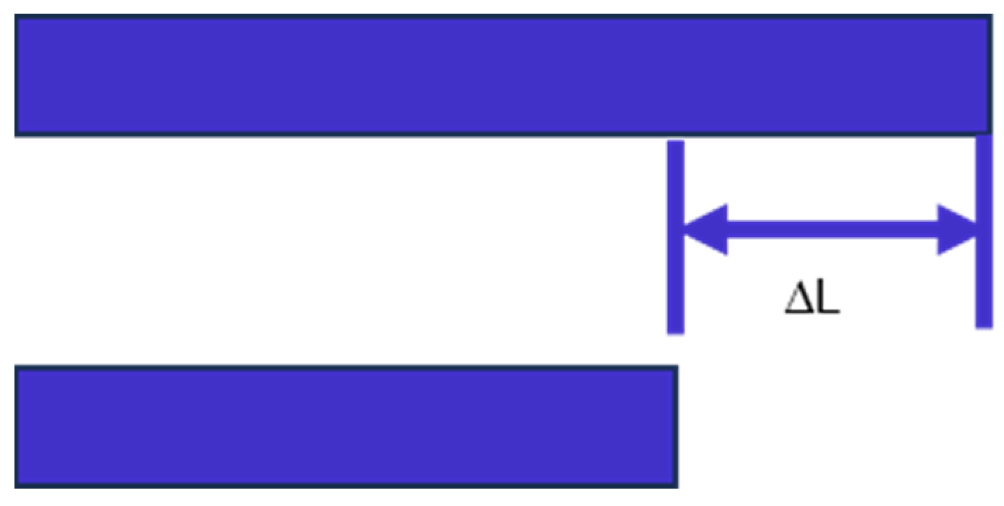
From the structure shown in Figure 2a, the design scheme of the device contains a 90° phase shifter. In this paper, the method of extending the length of the waveguide is used to introduce the phase shifter into the optical path, as shown in Figure 23. In the figure, represents the length difference between the two waveguides.

Figure 23.
Schematic diagram of the 90° phase shifter design scheme.
In an optical waveguide, the optical phase is expressed as:
where is the effective refractive index of the waveguide, and L is the waveguide length. Therefore, this paper can introduce a phase shift of 90° between the two waveguides by increasing the length of the waveguide:
Using the above Equation (17) this paper can get:
From the simulation, shown in Figure 5b, the effective refractive index of the waveguide is about 1.451 for a waveguide with a cross-section size of , and the value of is about 267 nm when the incident wavelength = 1550 nm, that is, the extended waveguide length is about 267 nm.
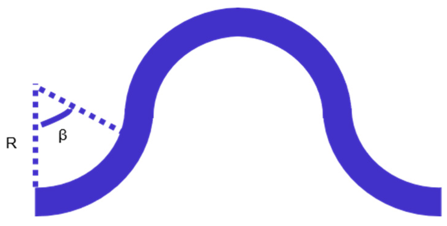
A schematic diagram of the connection section is shown in Figure 2c. By setting the length of the waveguide in the input and output areas of the 3 dB coupler and the distance between the upper and lower couplers of the two waveguides to 1000 μm, the length of the crossed waveguide can be calculated to be approximately 3863.70 μm, with a transverse length of about 3732.05 μm. To maintain the same optical path of the connection part, the other two connecting waveguides, except for the cross waveguide, are composed of four identical circular arcs, including the branch that introduces the 90° phase difference, as shown in Figure 24. Figure 24 indicates the radius R of each arc and the central angle β subtended by each arc. The length of the cross waveguide is 3863.70 μm, so the length of each arc is 965.93 μm. The bending radius of the semi-circular waveguide is 5000 μm, so the radian corresponding to each circular arc is converted to an angle of 11.0687°. When the 90° phase difference is introduced into the optical path, the length of the extended waveguide is about 267 nm, and the length of each arc is 966.18 μm. The bending radius of the semi-circular waveguide is 5000 μm, so the radian corresponding to each circular arc is converted to an angle of 11.0716°.

Figure 24.
Schematic diagram of the radius and the central angle of an arc.
2.8. Design Results
The design results of the above parameters are shown in Table 2.
Table 2.
Summary of design results.
As can be seen from Figure 2a, the length of the chip is determined by the length of the two 3 dB couplers and the transverse length of the intermediate connected waveguide. The width of the chip is primarily determined by the width and spacing of the two 3 dB couplers and the bending radius of the semi-circular waveguide. After conducting calculations based on the data in Table 2, it is concluded that the width of the chip is about 1230 μm, and the length of the chip is about 17212.05 μm. Considering the bending radius of the semi-circular waveguide, the size of the device is estimated to be around 17.5 mm × 1.6 mm.
Based on the previous description, we can know that the insertion loss of the 3 dB coupler is about 0.18 dB, the loss of the bending waveguide is about 0.58 dB/cm, and the cross loss of the crossed waveguide is about 0.12 dB. For a silicon dioxide straight waveguide with a refractive index difference of 0.75%, we take the transmission loss to be 0.03 dB/cm [39,40]. Combining the design results of the connection part, we can estimate the loss of the device at a wavelength of 1500 nm. When each of the two input ports of the structure shown in Figure 2a is supplied with a power of 1 unit, we can determine that the output power at each output port is 0.42. Thus, the total input power of the device () is 2, and the total output power is 1.68. It can be inferred that the total insertion loss of the device is approximately 0.8 dB.
3. Results
Based on the above determined parameters and from Equations (4)–(15), when the incident wavelength is 1550 nm, the four output signals to are shown in Figure 25. The horizontal axis of the figure is the input phase difference in rad, while the vertical axis is the output power of the four output ports. In the simulation, this paper assumes that each of the two input ports of the waveguide chip is supplied with a power of 1 unit. From Figure 25, it is observed that using the output phase of one port as a reference, the output phase of the in-phase port differs by 180°, while the output phases of the two out-of-phase ports differ by 90° and 270°, respectively. Additionally, the phases of the four outputs follow an orthogonal curve.
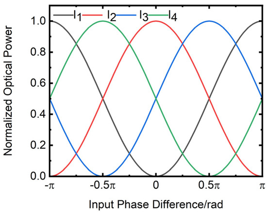
Figure 25.
Variation of four output power with input phase difference.
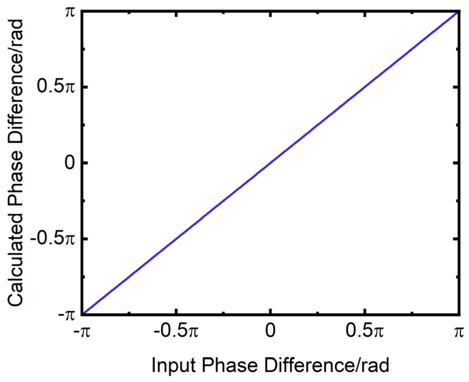
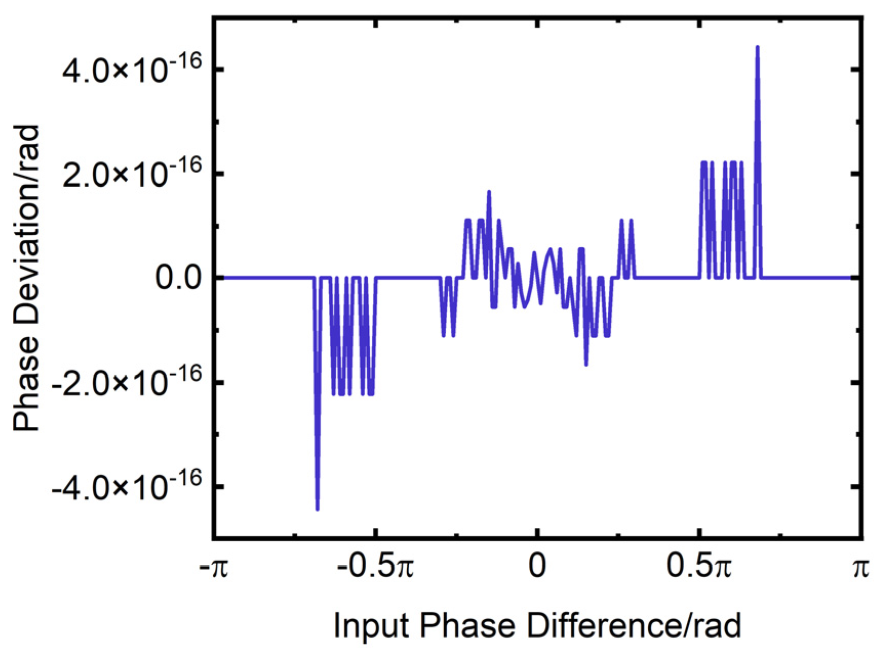
The calculated phase difference is presented in Figure 26. The horizontal axis of the figure is the input phase difference in rad, while the vertical axis is the calculated phase difference in rad. The deviation between the calculated phase difference and the input phase difference is illustrated in Figure 27. The horizontal axis of the figure is the input phase difference in rad, while the vertical axis is the phase deviation in rad. The Figure 27 demonstrate that the phase deviation is minimal and can be considered negligible.
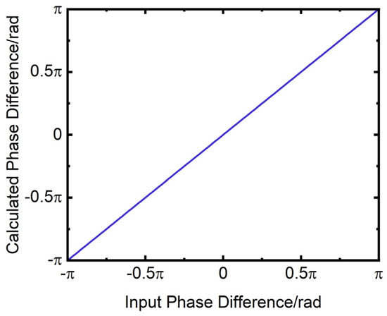
Figure 26.
Variation of calculated phase difference with input phase difference.
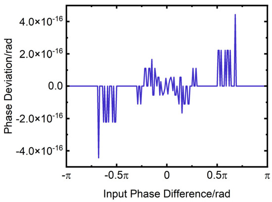
Figure 27.
Variation of phase deviation with input phase difference.
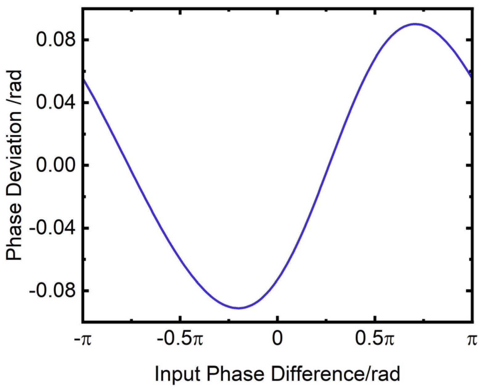
When performing simulation over a broadband wavelength range, this paper assumes that each of the two input ports of the waveguide chip is supplied with a power of 1 unit for each input wavelength. When the input wavelength range is 1.4 μm–1.7 μm, corresponding to a bandwidth is 300 nm, the power of the four outputs varies with the input phase difference and wavelength, as shown in Figure 28. In the figure, the x-axis represents the input wavelength in μm, the y-axis represents the input phase difference in rad, and the z-axis represents the normalized output power of the four output ports.
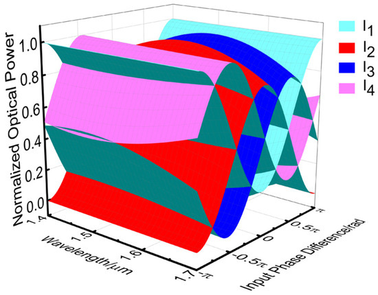
Figure 28.
Variation of quad output power with input phase difference and wavelength.
Figure 29 illustrates the variation in the normalized spectral intensity integral value of the four outputs with the input phase difference. In the simulation, this paper assumes that each of the two input ports of the waveguide chip is supplied with a power of 1 unit for the whole wavelength range. The horizontal axis of the figure is the input phase difference in rad, while the vertical axis is the normalized spectral intensity integral value of the four outputs.
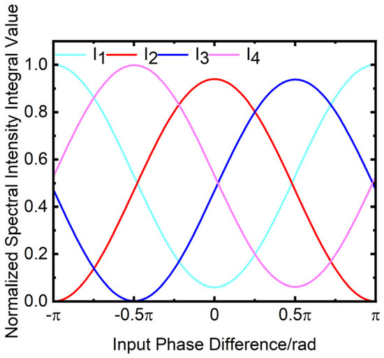
Figure 29.
Variation of quad spectral intensity integral value with input phase difference.
Figure 30 displays the variation in phase deviation with the input phase difference. The horizontal axis of the figure is the input phase difference in rad, while the vertical axis is the phase deviation in rad. As observed from Figure 30, when the incident optical bandwidth is 300 nm, the phase deviation varies in the range of −0.0912 rad to 0.0901 rad, which is equivalent to a phase deviation of approximately 5°. This level of accuracy meets the phase measurement requirements for optical interferometric imaging systems.
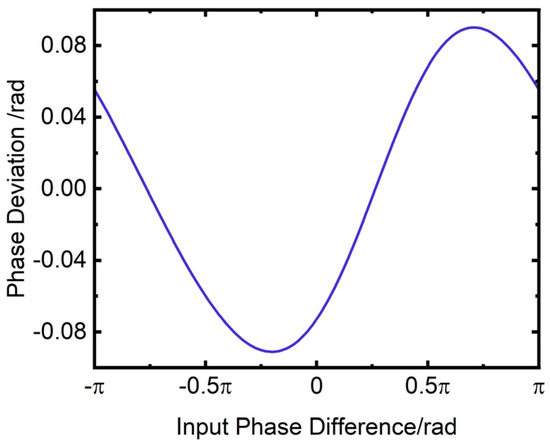
Figure 30.
Variation of phase deviation with input phase difference for a bandwidth of 300 nm.
4. Discussion
In this paper, the design of a broadband waveguide chip with phase measurement function is proposed. The device is designed to be approximately 17.5 mm × 1.6 mm in size, and the phase deviation is about 5° at a center wavelength of 1550 nm within the 300 nm wavelength range, and the loss of the device is approximately 0.8 dB. This indicates that the broadband waveguide chip with phase measurement function exhibits excellent performance, meeting the requirement for phase measurement deviation to remain within 0.18π. The proposed design is of great significance for improving the imaging quality of interferometric imaging systems, which can be applied to a variety of application scenarios, such as deep space exploration and ground monitoring. When the chip is applied to real scenarios, we recommend initially normalizing the actual optical power of the waveguide chip across the entire broadband wavelength range. This step standardizes the power values at different wavelengths, making the data comparable across wavelengths. Next, a peak-normalized scenario spectral curve should be introduced, which describes the relative intensity distribution of light sources at various wavelengths in the application scenario. The reason for introducing a peak-normalized scenario spectral curve is that, in practical applications, the spectral distribution of light sources is often uneven, and the light intensity at different wavelengths may vary significantly. Then, multiply the normalized waveguide chip power distribution by the peak-normalized scenario spectral curve. The purpose of this step is to combine the transmission characteristics of the waveguide chip at different wavelengths with the spectral distribution of actual light sources, thereby approximating the optical power distribution under real application conditions. This allows us to evaluate the chip’s performance in applications. With this design, we can anticipate substantial improvements in the imaging accuracy and resolution of interferometric systems, making it a valuable tool for both scientific research and practical applications. Additionally, this design will enable the collection of more accurate and detailed information about distant objects. Overall, the proposed design holds great potential for advancing imaging technology.
Author Contributions
Conceptualization, Y.L. and Q.Y.; methodology, Y.L.; software, Y.L.; validation, Y.L., Y.H. and C.Z.; formal analysis, Y.L.; investigation, Y.L.; resources, Q.Y. and S.S.; data curation, Y.L. and Q.Y.; writing—original draft preparation, Y.L.; writing—review and editing, Y.L. and Q.Y.; visualization, Y.L. and Q.Y.; supervision, Y.L., Y.H. and C.Z.; project administration, Q.Y.; funding acquisition, Q.Y. All authors have read and agreed to the published version of the manuscript.
Funding
This research was funded by National Natural Science Foundation of China, grant number 62105350.
Data Availability Statement
Data underlying the results presented in this paper are not publicly available at this time but may be obtained from the authors upon reasonable request. The data are not publicly available due to our institution does not support the release of the source code of self-developed computing software.
Acknowledgments
We express our sincere thanks to Jia liang Chen, Ben Ge and other fellow students at Shanghai Institute of Technical Physics of CAS, who reviewed the original paper and provided valuable comments.
Conflicts of Interest
The authors declare no conflicts of interest.
References
- Kendrick, R.L.; Duncan, A.; Ogden, C.; Wilm, J.; Stubbs, D.M.; Thurman, S.T.; Su, T.; Scott, R.P.; Yoo, S.J.B. Flat-panel space-based space surveillance sensor. In Proceedings of the Advanced Maui Optical and Space Surveillance Technologies Conference, Maui, HI, USA, 10–13 September 2013; p. 9. [Google Scholar]
- Chen, X.; Lin, J.; Wang, K. A Review of Silicon-Based Integrated Optical Switches. Laser Photonics Rev. 2023, 17, 2200571. [Google Scholar] [CrossRef]
- Taylor, M.G. Coherent detection method using DSP for demodulation of signal and subsequent equalization of propagation impairments. IEEE Photonics Technol. Lett. 2004, 16, 674–676. [Google Scholar] [CrossRef]
- Park, H.C.; Lu, M.; Bloch, E.; Reed, T.; Griffith, Z.; Johansson, L.; Coldren, L.; Rodwell, M. 40 Gbit/s coherent optical receiver using a Costas loop. Opt. Express 2012, 20, B197–B203. [Google Scholar] [CrossRef] [PubMed]
- Yoo, S.J. Low-Mass Planar Photonic Imaging Sensor. 2014. Available online: https://ntrs.nasa.gov/citations/20180003289 (accessed on 18 June 2024).
- Thurman, S.T.; Kendrick, R.L.; Duncan, A.; Wuchenich, D.; Ogden, C. System design for a SPIDER imager. In Frontiers in Optics; FM3E. 3; Optica Publishing Group: San Jose, CA, USA, 2015. [Google Scholar]
- Sbarufatti, C.; Beligni, A.; Gilioli, A.; Ferrario, M.; Mattarei, M.; Martinelli, M.; Giglio, M. Strain wave acquisition by a fiber optic coherent sensor for impact monitoring. Materials 2017, 10, 794. [Google Scholar] [CrossRef]
- Ge, B.; Yu, Q.; Chen, J.; Sun, S. Passive 3D Imaging Method Based on Photonics Integrated Interference Computational Imaging System. Remote Sens. 2023, 15, 2333. [Google Scholar] [CrossRef]
- Mansuripur, M. The van Cittert-Zernike Theorem. Opt. Photonics News 1999, 10, 38–42. [Google Scholar] [CrossRef]
- Blackledge, J.M. Digital Signal Processing: Mathematical and Computational Methods, Software Development and Applications; Elsevier: Amsterdam, The Netherlands, 2006. [Google Scholar]
- Chen, J.; Ge, B.; Yu, Q. Influence of measurement errors of the complex coherence factor on reconstructed image quality of integrated optical interferometric imagers. Opt. Eng. 2022, 61, 105108. [Google Scholar] [CrossRef]
- Duncan, A.; Kendrick, R.; Thurman, S.; Wuchenich, D.; Scott, R.P.; Yoo, S.J.; Su, T.; Yu, R.; Ogden, C.; Proiett, R. SPIDER: Next generation chip scale imaging sensor. In Proceedings of the Advanced Maui Optical and Space Surveillance Technologies Conference, Maui, HI, USA, 15–18 September 2015; p. 27. [Google Scholar]
- Badham, K.; Kendrick, R.L.; Wuchenich, D.; Ogden, C.; Chriqui, G.; Duncan, A.; Thurman, S.T.; Yoo, S.J.B.; Su, T.; Lai, W.; et al. Photonic integrated circuit-based imaging system for SPIDER. In Proceedings of the 2017 Conference on Lasers and Electro-Optics Pacific Rim (CLEO-PR), Singapore, 31 July–4 August 2017; pp. 1–5. [Google Scholar]
- Jain, P.; Honnungar, R.V. A review on materials for integrated optical waveguides. In Proceedings of Fourth International Conference on Inventive Material Science Applications: ICIMA 2021; Springer: Singapore, 2022; pp. 55–66. [Google Scholar]
- Butt, M.A. Integrated optics: Platforms and fabrication methods. Encyclopedia 2023, 3, 824–838. [Google Scholar] [CrossRef]
- Hoffman, D.; Heidrich, H.; Wenke, G.; Langenhorst, R.; Dietrich, E. Integrated optics eight-port 90 degrees hybrid on LiNbO3. J. Light. Technol. 1989, 7, 794–798. [Google Scholar] [CrossRef]
- Pan, P.; An, J.; Wang, H.; Wang, Y.; Zhang, J.; Wang, L.; Han, Q.; Hu, X. The design and error analysis of 90° hybrid based on InP 4 × 4 MMI. Opt. Commun. 2015, 351, 63–69. [Google Scholar] [CrossRef]
- Fandino, J.S.; Munoz, P. Manufacturing Tolerance Analysis of an MMI-Based 90° Optical Hybrid for InP Integrated Coherent Receivers. IEEE Photonics J. 2013, 5, 7900512. [Google Scholar] [CrossRef]
- Yagi, H.; Inoue, N.; Masuyama, R.; Kikuchi, T.; Katsuyama, T.; Tateiwa, Y.; Uesaka, K.; Yoneda, Y.; Takechi, M.; Shoji, H. InP-Based pin-Photodiode Array Integrated with 90° Hybrid Using Butt-Joint Regrowth for Compact 100 Gb/s Coherent Receiver. IEEE J. Sel. Top. Quantum Electron. 2014, 20, 374–380. [Google Scholar] [CrossRef]
- Pennings, E.C.M.; Deri, R.J.; Bhat, R.; Hayes, T.R.; Andreadakis, N.C. Ultracompact, all-passive optical 90 degrees-hybrid on InP using self-imaging. IEEE Photonics Technol. Lett. 1993, 5, 701–703. [Google Scholar] [CrossRef]
- Soldano, L.B.; Pennings EC, M. Optical multi-mode interference devices based on self-imaging: Principles and applications. J. Light. Technol. 1995, 13, 615–627. [Google Scholar] [CrossRef]
- Inoue, T.; Nara, K. Ultrasmall PBS-integrated coherent mixer using 1.8%-delta silica-based planar lightwave circuit. In Proceedings of the 36th European Conference and Exhibition on Optical Communication, Turin, Italy, 19–23 September 2010; pp. 1–3. [Google Scholar]
- Halir, R.; Roelkens, G.; Ortega-Moñux, A.; Wangüemert-Pérez, J.G. High-performance 90 hybrid based on a silicon-on-insulator multimode interference coupler. Opt. Lett. 2011, 36, 178–180. [Google Scholar] [CrossRef]
- Yang, W.; Yin, M.; Li, Y.; Wang, X.; Wang, Z. Ultra-compact optical 90° hybrid based on a wedge-shaped 2 × 4 MMI coupler and a 2× 2 MMI coupler in silicon-on-insulator. Opt. Express 2013, 21, 28423–28431. [Google Scholar] [CrossRef]
- Jiang, Q.Y. Study on Fabrication Tolerance of Broadband Silicon Photonic Directional Couplers; Nanjing University: Nanjing, China, 2020. [Google Scholar]
- Huang, W.-P. Coupled-mode theory for optical waveguides: An overview. JOSA A 1994, 11, 963–983. [Google Scholar] [CrossRef]
- Cha, Y. Research on Silica-on-Silicon Matrix Optical Switches Based on Planar Lightwave Circuit; Tianjin University: Tianjin, China, 2007. [Google Scholar]
- Voigt, K.; Zimmermann, L.; Winzer, G.; Tian, H.; Tillack, B.; Petermann, K. C-Band Optical 90° Hybrids in Silicon Nanowaveguide Technology. IEEE Photonics Technol. Lett. 2011, 23, 1769–1771. [Google Scholar] [CrossRef]
- Suzuki, K.; Takiguchi, K.; Hotate, K. Monolithically integrated resonator microoptic gyro on silica planar lightwave circuit. J. Light. Technol. 2000, 18, 66–72. [Google Scholar] [CrossRef]
- Qiu, C.; Wang, Y.B.; Chen, Y.Y.; Lei, Y.X.; Qin, L.; Wang, L.J. Design and analysis of a novel graphene-assisted silica/polymer hybrid waveguide with thermal–optical phase modulation structure. IEEE Photonics J. 2019, 11, 1–10. [Google Scholar] [CrossRef]
- Wang, J.; Kroh, M.; Theurer, A.; Zawadzki, C.; Schmidt, D.; Ludwig, R.; Lauermann, M.; Zhang, Z.; Beling, A.; Matiss, A.; et al. Dual-quadrature coherent receiver for 100 G Ethernet applications based on polymer planar lightwave circuit. Opt. Express 2011, 19, B166–B172. [Google Scholar] [CrossRef] [PubMed]
- Zhai, Y.; Wang, J.; Xu, J.; Lu, Y. Polymeric multi-mode interference based optical 90° hybrid with tolerant performance. In Proceedings of the 2015 14th International Conference on Optical Communications and Networks (ICOCN), Nanjing, China, 3–5 July 2015; pp. 1–3. [Google Scholar]
- Agrawal, G.P. Fiber-Optic Communication Systems; John Wiley & Sons: New York, NY, USA, 2012. [Google Scholar]
- Poulsen, M.R.; Borel, P.I.; Fage-Pedersen, J.; Hübner, J.R.; Kristensen, M.; Povlsen, J.H.; Rottwitt, K.; Svalgaard, M.; Svendsen, W. Advances in silica-based integrated optics. Opt. Eng. 2003, 42, 2821–2834. [Google Scholar] [CrossRef]
- Haowen, S.; Zhaotang, S.; Xingjun, W.; Zhiping, Z. Recent progress of silicon photonics for middle-infrared application. Telecommun. Sci. 2015, 31, 2015274. [Google Scholar]
- Li, Y.P.; Henry, C.H. Silica-based optical integrated circuits. IEE Proc. Optoelectron. 1996, 143, 263–280. [Google Scholar] [CrossRef]
- Song, Q.Q. Research on Integrated Optical Waveguide Switches and Tunable Delay Lines; School of Optoelectronic Science and Engineering: Chengdu, China, 2021. [Google Scholar]
- Koai, K.T.; Liu, P.L. Modeling of Ti: LiNbO3 waveguide devices. II. S-shaped channel waveguide bends. J. Light. Technol. 1989, 7, 1016–1022. [Google Scholar] [CrossRef]
- Goh, T.; Yasu, M.; Hattori, K.; Himeno, A.; Okuno, M.; Ohmori, Y. Low loss and high extinction ratio strictly nonblocking 16/spl times/16 thermooptic matrix switch on 6-in wafer using silica-based planar lightwave circuit technology. J. Light. Technol. 2001, 19, 371–379. [Google Scholar] [CrossRef]
- Suzuki, S.; Yanagisawa, M.; Hibino, Y.; Oda, K. High-density integrated planar lightwave circuits using SiO2-GeO2 waveguides with a high refractive index difference. SPIE Milest. Ser. MS 1996, 125, 133–139. [Google Scholar]


Disclaimer/Publisher’s Note: The statements, opinions and data contained in all publications are solely those of the individual author(s) and contributor(s) and not of MDPI and/or the editor(s). MDPI and/or the editor(s) disclaim responsibility for any injury to people or property resulting from any ideas, methods, instructions or products referred to in the content. |
© 2024 by the authors. Licensee MDPI, Basel, Switzerland. This article is an open access article distributed under the terms and conditions of the Creative Commons Attribution (CC BY) license (https://creativecommons.org/licenses/by/4.0/).