Article

Atomic Layer Deposition of Ultrathin La2O3/Al2O3 Nanolaminates on MoS2 with Ultraviolet Ozone Treatment

1
School of Materials Science and Engineering, Chang’an University, Xi’an 710061, China
2
Key Laboratory of Wide Band-Gap Semiconductor Materials and Devices, School of Microelectronics, Xidian University, Xi’an 710071, China
*
Author to whom correspondence should be addressed.
Materials 2022, 15(5), 1794; https://doi.org/10.3390/ma15051794
Submission received: 25 January 2022 / Revised: 21 February 2022 / Accepted: 25 February 2022 / Published: 27 February 2022
(This article belongs to the Section Thin Films and Interfaces)

Abstract

:
Due to the chemically inert surface of MoS2, uniform deposition of ultrathin high-κ dielectric using atomic layer deposition (ALD) is difficult. However, this is crucial for the fabrication of field-effect transistors (FETs). In this work, the atomic layer deposition growth of sub-5 nm La2O3/Al2O3 nanolaminates on MoS2 using different oxidants (H2O and O3) was investigated. To improve the deposition, the effects of ultraviolet ozone treatment on MoS2 surface are also evaluated. It is found that the physical properties and electrical characteristics of La2O3/Al2O3 nanolaminates change greatly for different oxidants and treatment processes. These changes are found to be associated with the residual of metal carbide caused by the insufficient interface reactions. Ultraviolet ozone pretreatment can substantially improve the initial growth of sub-5 nm H2O-based or O3-based La2O3/Al2O3 nanolaminates, resulting in a reduction of residual metal carbide. All results indicate that O3-based La2O3/Al2O3 nanolaminates on MoS2 with ultraviolet ozone treatment yielded good electrical performance with low leakage current and no leakage dot, revealing a straightforward approach for realizing sub-5 nm uniform La2O3/Al2O3 nanolaminates on MoS2.

1. Introduction

Silicon complementary metal-oxide-semiconductor (CMOS) devices continuing shrink in size, and keeping the generation of heat low has becoming extremely challenging [1,2]. One promising alternative approach is to use transition metal dichalcogenides (TMDs) due to their extraordinary electronic and mechanical properties [3,4]. Particularly, molybdenum disulfide (MoS2) with a natural bandgap (1.2~1.8 eV) has attracted plenty of researches for its promising application in scaled low-power field effect transistors (FETs) and flexible devices [5,6]. A crucial step in the manufacturing of FETs is the growth of ultrathin and uniform high-k gate dielectric on MoS2. The mobility of MoS2 can be further improved after high-k gate films deposition through the suppression of Coulomb scattering by the dielectric mismatch effect between the MoS2 and high-k dielectric [7,8]. The most controlled approach for obtaining nanoscale, high-quality growth of dielectrics is atomic layer deposition (ALD). However, atomic layer deposition of ultrathin and uniform high-k gate films on MoS2 still represents one of the key challenges to be addressed due to the lack of dangling bonds or nucleation sites on the MoS2 surface. The physical adsorption of precursors on the surface is considered to be a key element that enables the initial ALD reaction to take place [9]. Nevertheless, the weakly physical adsorption of precursors can be easily desorbed from the surface by the subsequent purge gas [10]. The dielectric films easy to form pinhole-like defects when it is directly deposited on MoS2 due to random nucleation at defects, edges, and impurities, especially the thickness of the dielectric less than a few nanometers [11]. However, to meet the demand of ultra-scaled FETs, the thickness of gate dielectric layer needs to be extremely thin (<5 nm) for sufficient electrostatic coupling of the gate to the semiconducting channel [12].
To cope with these challenges, the pretreatment of a MoS2 surface with oxygen plasma [13], introduction of an additional seeding layer [14], ultraviolet ozone (UV-O3) [15], water plasma treatment [16] have been demonstrated. Growth of sub-5 nm uniform Al2O3 film on MoS2 has been achieved [12]. La2O3 has a high dielectric constant (~26), large band gap (~5.8 eV), and the drawback of moisture absorption can be greatly improved by mixed with a less hygroscopic oxide Al2O3 [17,18]. It has been studied as the candidate gate dielectric in the sub-22 nm technical process node. The La2O3/Al2O3 nanolaminate processed film can provide a higher dielectric constant and better leakage current control at the same physical thickness compared to the Al2O3 film. However, to date, the growth of La-based binary or ternary compounds on MoS2 has not been investigated. Therefore, in this paper, the ALD deposition of sub-5 nm La2O3/Al2O3 nanolaminates on MoS2 is carried out and the properties of La2O3/Al2O3 nanolaminates on MoS2 are investigated.

2. Materials and Methods

In the experiment, n-type silicon (100) wafers with a resistivity of 2–4 Ω·cm were cleaned by RCA method and a 60 s dip in diluted HF solution was used to remove the native oxide, followed by 5 min of washing with deionized water. Then, the silicon wafers were immediately transferred to an ultra-high vacuum RF magnetron sputtering system chamber and a MoS2 target was cleaned in 10 min by pre-sputtering under the deposition conditions. Afterward, few layers MoS2 film was directly deposited by RF magnetron sputtering system with the RF power of 50 W at 400 °C. For sulfur compensation and defects reduction, all wafers were annealed in the hydrogen sulfide at 700 °C for 60 min. After that, some wafers were treated by UV ozone ProCleaner plus system under the power of 11.04 mW·m−2 for 5 min at the room temperature to improve the surface of MoS2. The Raman spectra of MoS2 before and after UV-O3 treatment is shown in Figure 1. The two characteristics Raman modes (A1g and E12g) of the MoS2 can be observed and their positions changed negligibly before and after UV-O3 treatment. It indicates that the treatment causes minimal structural damage in MoS2. Moreover, the difference between these two peaks is 27.3 cm−1, which indicated that the thickness of MoS2 is between five and seven layers [19].
Then, the wafers with or without UV-O3 treatment were transferred to the ALD chamber to deposited La2O3/Al2O3 nanolaminates at 260 °C. Tris (isopropylcyclopentadienyl) lanthanum (La(iPrCp)3) and trimethyl-aluminum (TMA) was used as the lanthanum and aluminum precursor, respectively. H2O and O3 was used as the oxidant, respectively. O3 was generated by the ozone generator using ultra-pure O2 (99.999%).10 deposition sequence cycles of TMA/H2O/La(iPrCp)3/H2O and TMA/O3/La(iPrCp)3/O3 were used to obtain H2O-based La2O3/Al2O3 nanolaminates and O3-based La2O3/Al2O3 nanolaminates, respectively. Before the ALD deposition sequence, a 4 s pulse time of TMA was carried out firstly to form the physical adsorption on the surface. ~3 nm H2O-based La2O3/Al2O3 nanolaminates and O3-based La2O3/Al2O3 nanolaminates were measured by Woollam M2000D spectroscopic ellipsometry. After O3-based and H2O-based La2O3/Al2O3 nanolaminates deposition process, Al electrode was fabricated by photolithography patterning to form MOS capacitors after back Al electrode was prepared by magnetron sputtering. Atomic force microscopy (AFM, Bruker Dimension Edge, Bruker Nano Inc., Billerica, WA, USA), X-ray photoelectron spectroscopy (XPS, Thermo Scientific K-Alpha, Thermo Fisher Scientific Inc., Waltham, MA, USA) were used to character the properties of La2O3/Al2O3 nanolaminates on MoS2. The standard electrical measurements were performed at room temperature using the Keithley 4200SCS characterization system (Tektronix Inc., Kent, WA, USA).

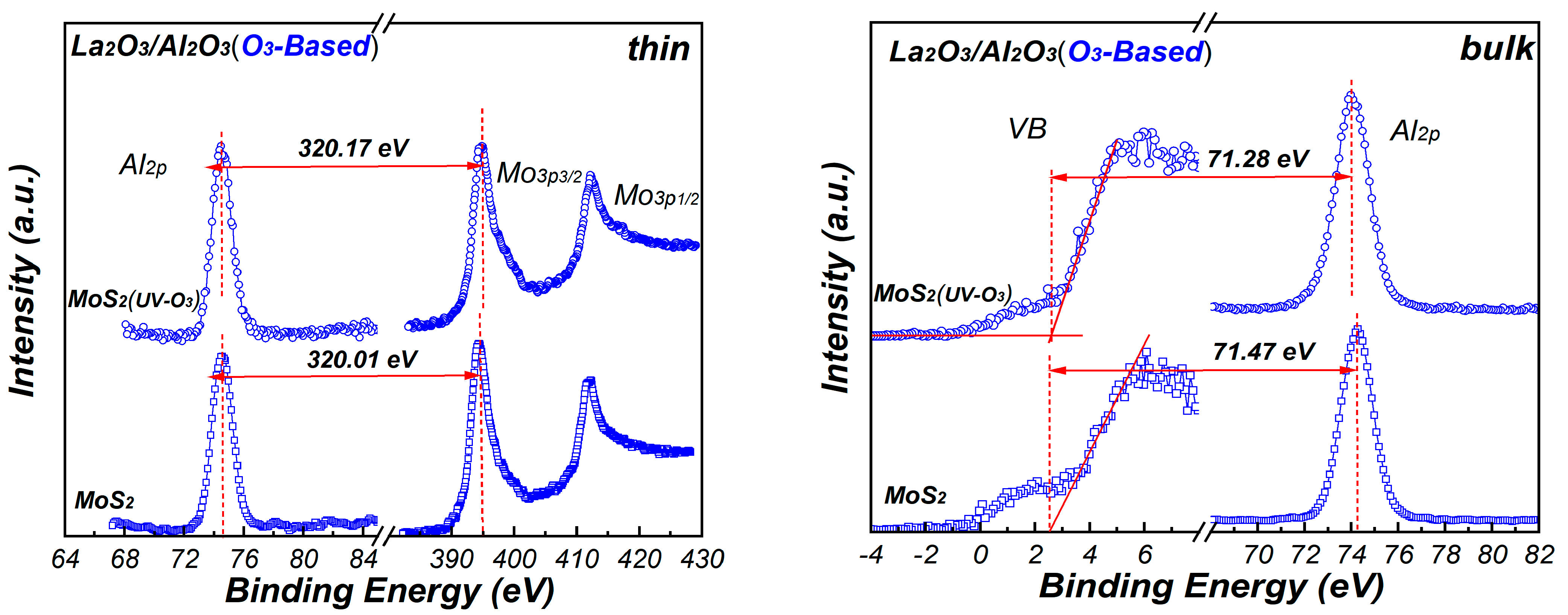
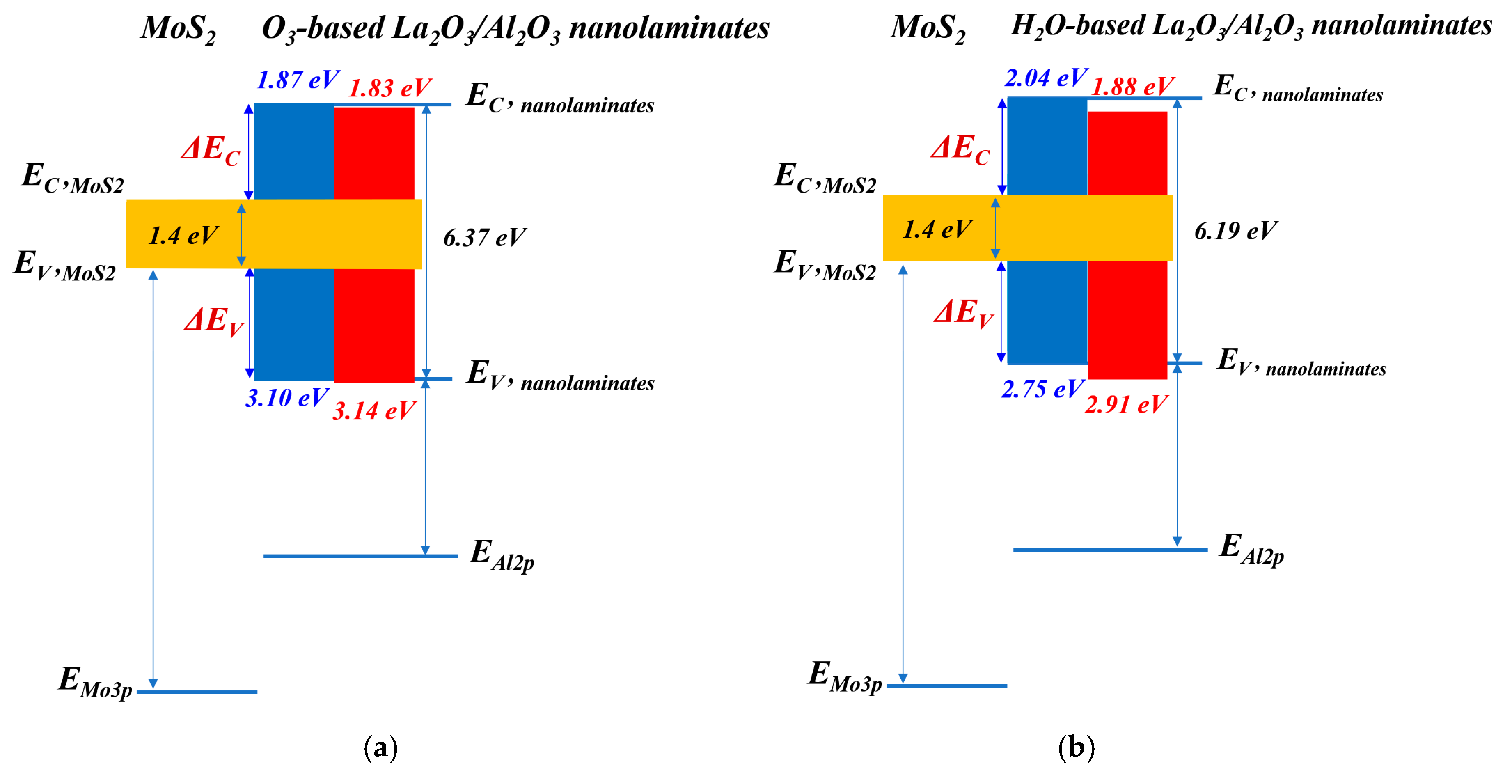
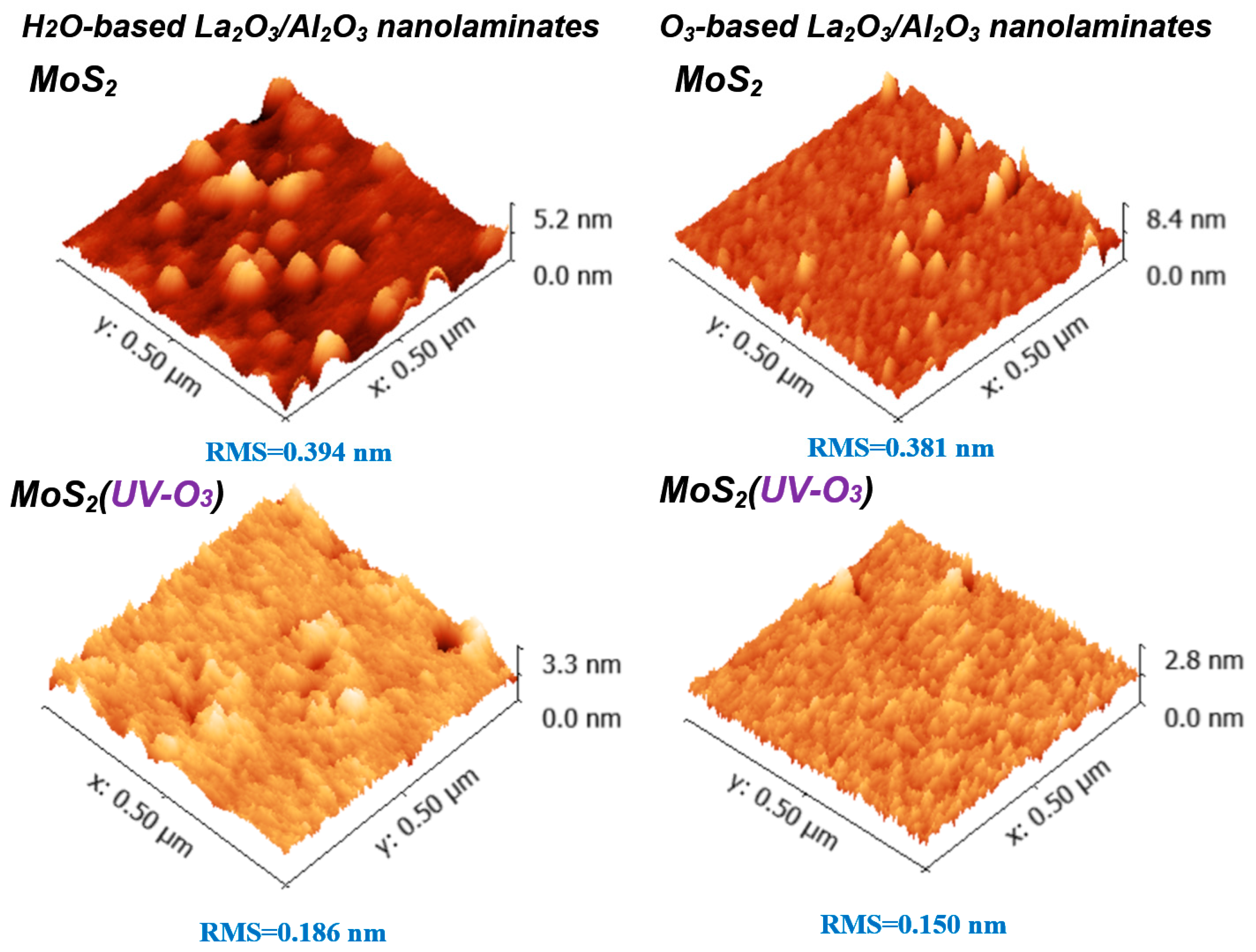
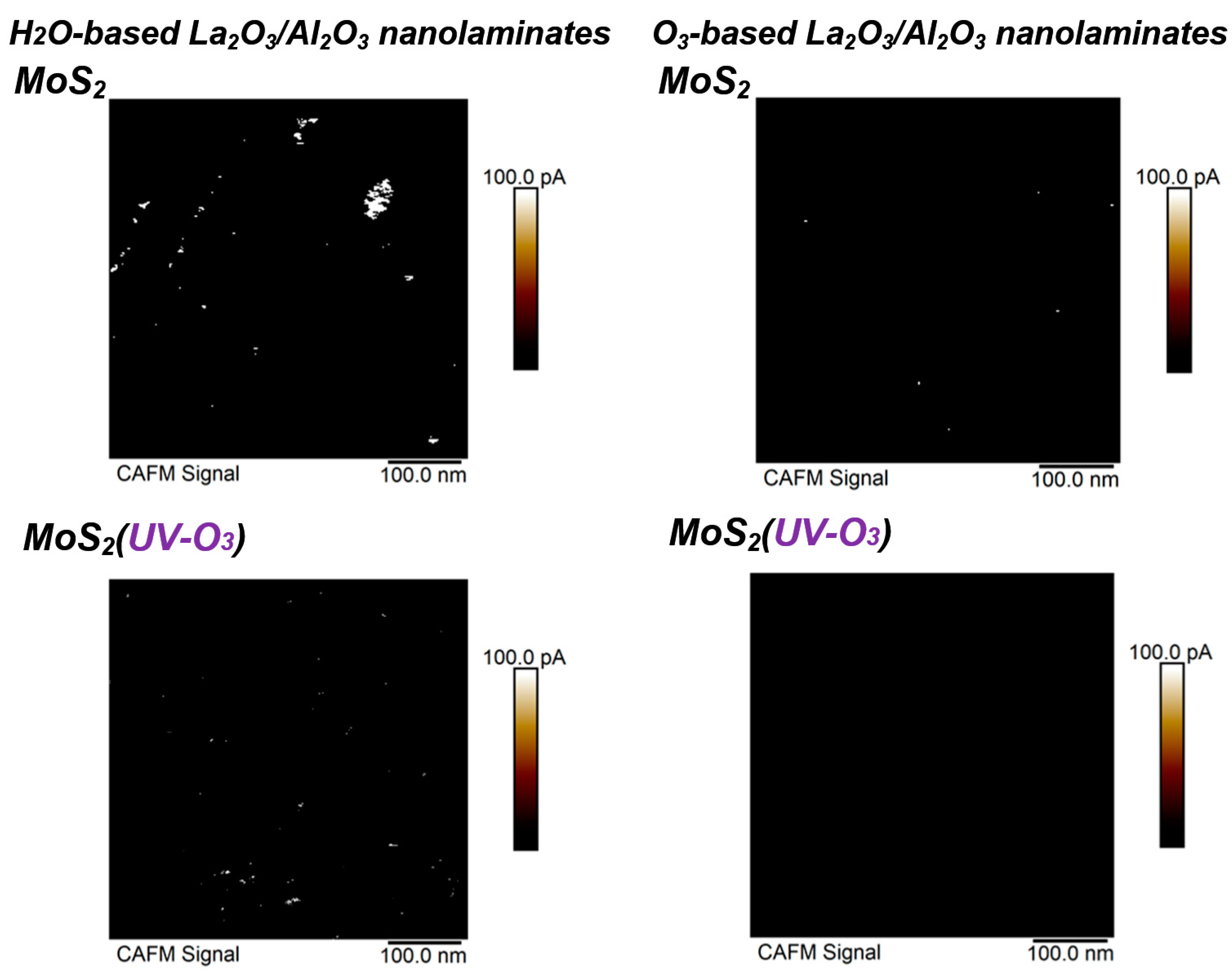
3. Results and Discussion

Figure 2 shows the AFM results of La2O3/Al2O3 nanolaminates on MoS2. It can be found that non-uniformity surface is observed for both O3-based and H2O-based La2O3/Al2O3 nanolaminates on MoS2, which indicates that it is difficult to grow uniform ultrathin dielectric directly on MoS2. Meanwhile, a smoother surface is obtained for O3-based La2O3/Al2O3 nanolaminates compared to H2O-based La2O3/Al2O3 nanolaminates on MoS2. This may be explained by that, O3 has higher reactivity due to its strong oxidizing ability, it is easy to decompose to O2 and monatomic O during the ALD reactions, the monatomic O radical diffusion and desorption will significantly affect the growth of the film. Using ozone as oxidant enhances the Al2O3 film coverage and uniformity on MoS2 due to ozone facilitates initial TMA precursor nucleation on the MoS2 [20], which is consistent with the AFM results. After MoS2 treated with UV-O3, the improvement of the uniform surface is observed for both O3-based and H2O-based La2O3/Al2O3 nanolaminates (and especially for O3-based La2O3/Al2O3 nanolaminates). The root mean square (RMS) value of O3-based La2O3/Al2O3 nanolaminates decreases from 0.381 nm to 0.150 nm, while the RMS value of H2O-based La2O3/Al2O3 nanolaminates decreases from 0.394 nm to 0.186 nm after MoS2 suffered from UV-O3 treatment. Generally, the lack of reaction surface for MoS2 lead to an increase of surface roughness after ALD deposition due to the buildup of precursors and reaction products randomly occurred [11]. The improvement of uniform and decrease of RMS value suggest that the initial surface nucleation of ultrathin La2O3/Al2O3 nanolaminates on MoS2 can be improved by UV-O3 treatment.
To evaluate the dielectric electrical properties with nanometer resolution, conductive AFM measurements are carried out by applying a constant voltage between the Pt-Ir coated tip and sample. Figure 3 shows the current images measured by conductive AFM when applying a sample bias of 1 V. As shown in Figure 3, the density of leakage dots in the H2O-based La2O3/Al2O3 nanolaminates is higher than that in the O3-based La2O3/Al2O3 nanolaminates. The leakage dot is an indicator of conductive paths exist in La2O3/Al2O3 nanolaminates. They are not only attributed to surface roughness, but also possibly caused by local fluctuations in composition and/or structures, and/or by defects in La2O3/Al2O3 nanolaminates [21]. The presence of many leakage dots indicates that H2O-based La2O3/Al2O3 nanolaminates on MoS2 is not suitable for use as a gate dielectric layer. After MoS2 treated with UV-O3 treatment, the leakage dots for both O3-based and H2O-based La2O3/Al2O3 nanolaminates decreased. In particular, no leakage dot is observed for O3-based La2O3/Al2O3 nanolaminates. It indicates that, with the help of UV-O3 treatment, ultrathin O3-based La2O3/Al2O3 nanolaminates on MoS2 can serve as the gate dielectric due to its good leakage suppression properties.
The changes in uniformity of La2O3/Al2O3 nanolaminates on MoS2 may be originated from the interface due to the ALD process of growing La2O3/Al2O3 nanolaminates on silicon is well established [17]. To reveal the changes that occurred at the interface, XPS measurements are performed. Figure 4 shows the C1s spectra of La2O3/Al2O3 nanolaminates on MoS2. There are mainly two peaks in the C1s spectra for all La2O3/Al2O3 nanolaminates on MoS2, which are located at binding energies of 283.0 eV and 284.8 eV. These peaks correspond to the metal carbide and adsorbed carbon, respectively [22]. Moreover, the peak intensity of metal carbide in H2O-based ALD process decreases from 30.0 a.t.% to 15.8 a.t.% after MoS2 suffered from UV-O3 treatment, while that of O3-based ALD process decreases from 11.9 a.t.% to 9.8 a.t.%. The lowest metal carbide content in O3-based La2O3/Al2O3 nanolaminates on MoS2 with UV-O3 treatment suggests that the initial interfacial reactions are greatly improved. The appearance of metal carbide is an indication that poor interface reactions occur during the ALD process, which can originate from the generation of intermediates or by-products of metal precursors. MoS2 suffered from low-power UV-O3 treatment form the weak chemical bond of S-O on the surface without hampering its electrical performance [15], which can supply the reaction interface groups at the MoS2 surface during the ALD deposition. As a result, the residuals of the metal carbide or its intermediate precursor during the first ALD reaction cycles can be reduced and the roughness of the nanolaminates can be improved.
In order to further confirm the residue in La2O3/Al2O3 nanolaminates on MoS2, Figure 5 shows the Al2p spectra of La2O3/Al2O3 nanolaminates on MoS2. As shown in Figure 5, the Al2p spectra can be fitted to two peaks, which located at the binding energy of ~74.6 eV and 73.8 eV, respectively. 74.6 eV belongs to the Al-O bond, and the lower 73.8 eV is related to carbide [22]. The content of carbide in H2O-based La2O3/Al2O3 nanolaminates decreases from 9.66 a.t.% to 3.88 a.t.% after MoS2 treated with UV-O3 treatment, while that of O3-based La2O3/Al2O3 nanolaminates decreases from 2.98 a.t.% to 0.92 a.t.% after MoS2 treated with UV-O3 treatment. The variation of carbide content in La2O3/Al2O3 nanolaminates on MoS2 is consistent with the C1s results. Due to lack of dangling bonds or nucleation sites on MoS2, the initial reaction of ALD is dependent on weakly physical adsorbed TMA precursors on MoS2 surface. UV-O3 treatment forms the weak S-O bonds on MoS2 and facilitates the uniform physical adsorption of precursor, which is beneficial for the improvement of initial ALD self-limiting surface reactions. O3 has a stronger ability than water to split the C-H or Al-C bonds which attached to metal atoms in the deposition [18]. As a result, the concentration of metal carbide in O3-based La2O3/Al2O3 nanolaminates is lower than H2O-based La2O3/Al2O3 nanolaminates.
To determine the valence band offset (VBO) between La2O3/Al2O3 nanolaminates and MoS2, the Kraut method is used which discussed in ref. [23],
Δ E V B O = ( E C L M o 3 p E V ) b u l k , M o S 2 ( E C L A l 2 p E V ) t h i c k   n a n o l a m i n a t e s ( E C L M o 3 p E C L A l 2 p ) t h i n   n a n o l a m i n a t e s / M o S 2
where E C L M o 3 p and   E C L A l 2 p is the binding energy of the Mo3p and Al2p shallow core levels, respectively. Ev is the binding energy corresponding to the valence band maximum (VBM). The value of VBM is determined by the intercept of the slope at the leading edge of the valence band spectrum with the base line. To correct the differential charging, the binding energy calibration was performed using a gold standard sample. Figure 6 shows the core level spectra of ~10 nm sputtered MoS2 with or without UV-O3 treatment. The energy difference between the Mo3p core level and the VBM is 394.58 eV and 394.59 eV for the clean MoS2 and MoS2 treated with UV-O3 treatment, respectively. These values are agreed well with the values reported in ref. [24].
Figure 7 shows the XPS core level spectra of Mo3p and Al2p for La2O3/Al2O3 nanolaminates. The core level energies are obtained by curve fitting to ensure high accuracy binding energy of the peak. In order to measure the band offset between La2O3/Al2O3 nanolaminates and MoS2, ~10 nm H2O-based and O3-based La2O3/Al2O3 nanolaminates are prepared for use as bulk films, respectively. As shown in Figure 7, the energy difference values between the core level energies are determined. Using these energy difference values with Equation (1), the VBO values of the H2O-based and O3-based La2O3/Al2O3 nanolaminates on MoS2 can be derived. The VBO of 3.10 eV and 3.14 eV is obtained for O3-based La2O3/Al2O3 nanolaminates on MoS2 and MoS2 with UV-O3 treatment, respectively. In addition, the VBO of H2O-based nanolaminates on MoS2 and MoS2 with UV-O3 treatment is 2.75 eV and 2.91 eV, respectively. The results indicate that the VBO is affected by the different oxidants and UV-O3 treatment. The negligible VBO variations for O3-based La2O3/Al2O3 nanolaminates suggest that it has a better stability compared to H2O-based La2O3/Al2O3 nanolaminates.
To obtain the conduction band offset (CBO) between La2O3/Al2O3 nanolaminates and MoS2, the optical band gaps of La2O3/Al2O3 nanolaminates are measured. The optical band gaps form the plots of (αE)2 versus photo energy E are shown in Figure 8. The extrapolation of the linear part of (αE)2 –E down to (αE)2 = 0 gives the values of band gaps [25]. The measured band gap value of O3-based and H2O-based La2O3/Al2O3 nanolaminates is 6.37 eV and 6.19 eV, respectively. These values are in good agreement with the reported values of La2O3/Al2O3 gate stack or LaAlO3 films ranging from 6.1–6.4 eV [17,26]. The results indicate that the O3-based La2O3/Al2O3 nanolaminates has a lager bandgap value compared to the H2O-based nanolaminates. This may be caused by the lower content of impurities found in O3-based La2O3/Al2O3 nanolaminates compared to H2O-based nanolaminates.
Using the calculated VBO and band gap values, the conduction band offset between La2O3/Al2O3 nanolaminates and MoS2 can be attained by the following equation:
Δ E C B O = E g La 2 O 3 / Al 2 O 3   nanolaminates E g M o S 2 Δ E V B O
where E g La 2 O 3 / Al 2 O 3   nanolaminates and E g M o S 2 is the bandgap of La2O3/Al2O3 nanolaminates and MoS2, respectively. The bandgap of 1.4 eV for MoS2 is used here [27]. According to the Equation (2), the CBO of O3-based La2O3/Al2O3 nanolaminates on MoS2 and MoS2 with UV-O3 treatment is 1.87 eV and 1.83 eV, respectively. Meanwhile, the CBO of H2O-based La2O3/Al2O3 nanolaminates on MoS2 and MoS2 with UV-O3 treatment is 2.04 eV and 1.88 eV, respectively. The corresponding band diagrams are illustrated in Figure 9. It can be seen that both La2O3/Al2O3 nanolaminates/MoS2 interface have a Type I alignment, where the conduction band edge and valence band edge of MoS2 are located within the bandgap of La2O3/Al2O3 nanolaminates. Furthermore, both CBO and VBO values of La2O3/Al2O3 nanolaminates on MoS2 provide excellent electron and hole barriers due to their values larger than 1 eV, ensuring La2O3/Al2O3 nanolaminates suitability for FETs applications. Remarkably, O3-based La2O3/Al2O3 nanolaminates has a higher VBO compare with H2O-based La2O3/Al2O3 nanolaminates, which is better for p-channel FETs application.
Figure 10 shows the I-V curves of La2O3/Al2O3 nanolaminates on MoS2 after fabricated metal-oxide-semiconductor (MOS) capacitor. At the applied voltage of 2 V, for O3-based La2O3/Al2O3 nanolaminates, the leakage current decreased from 1.2 × 10⁻² mA to 9.6 × 10⁻³ mA, while the breakdown voltage increased from 9.01 V to 10.21 V after MoS2 treated with UV-O3 treatment. The same trend is observed in H2O-based La2O3/Al2O3 nanolaminates. The leakage current decreased from 2.6 × 10⁻² mA to 2.3 × 10⁻² mA, while the breakdown voltage increased from 6.76 V to 7.36 V after MoS2 treated with UV-O3 treatment. The breakdown voltage is obtained when the leakage current reaches 1 mA [28]. The decease of leakage current and increase of breakdown voltage may be attributed to the uniformity of the La2O3/Al2O3 nanolaminates as well as the reduction of impurities or residuals at the interface. The leakage current may originate either Poole-Frenckel or Fowler-Nordheim mechanism from the point of view of quantum tunneling [29,30], which has been confirmed in our measurement. The lowest leakage current and highest breakdown voltage are obtained for O3-based La2O3/Al2O3 nanolaminates on MoS2 with UV-O3 treatment, making it a promising dielectric candidate for the application of MoS2 FETs.

4. Conclusions

In this study, atomic layer deposition growth of sub-5 nm La2O3/Al2O3 nanolaminates on MoS2 using different oxidants (H2O and O3) and the UV-O3 pretreatment on MoS2 are investigated. Compared with H2O-based La2O3/Al2O3 nanolaminates on MoS2, better uniformity and lower leakage dots were observed for O3-based La2O3/Al2O3 nanolaminates on MoS2. This is associated with the metal carbide concentration in La2O3/Al2O3 nanolaminates on MoS2, which is generated by insufficient interfacial reactions. UV-O3 treatment can decrease the residuals of the metal carbide and improve the deposition of La2O3/Al2O3 nanolaminates on the MoS2 interface by introducing the weak S-O bonds to MoS2 surface, leading to the properties of La2O3/Al2O3 nanolaminates being substantially improved. The band offset values of both O3-based and H2O-based La2O3/Al2O3 nanolaminates/MoS2 are larger than 1 eV, which can provide eligible electron and hole barrier height. In particular, a higher valence band offset is obtained for O3-based La2O3/Al2O3 nanolaminates compared to H2O-based La2O3/Al2O3 nanolaminates. Consequently, O3-based La2O3/Al2O3 nanolaminates on MoS2 exhibits smaller leakage current and higher breakdown voltage, especially after MoS2 suffered from UV-O3 treatment. All results indicate that O3-based La2O3/Al2O3 nanolaminates on MoS2 with UV-O3 treatment is a more appropriate process to obtain sub-5 nm uniform La2O3/Al2O3 nanolaminates on MoS2 due to its good electrical characteristics, providing important implications for its integration into transistors.

Author Contributions

J.F. performed the data analyses and wrote the manuscript; Y.S., performed the experiment; H.L., S.W. and L.D. helped perform the analysis with constructive discussions; L.L., Y.Z. and X.W. contributed to the conception of the study. All authors have read and agreed to the published version of the manuscript.

Funding

This work was supported by the National Natural Science Foundation of China (Grant Nos. 61604016, 51501017 and 51802025), China Postdoctoral Science Foundation (Grant No. 2017M613028), Natural Science Foundation of Shaanxi Province, China (2021GY-255), the Fundamental Research Funds for the Central Universities (Grant No. 300102319209).

Institutional Review Board Statement

Not applicable.

Informed Consent Statement

Not applicable.

Data Availability Statement

Data will be made available upon reasonable request.

Conflicts of Interest

The authors declare no conflict of interest.

References

  1. Maurand, R.; Jehl, X.; Kotekar-Patil, D.; Corna, A.; Bohuslavskyi, H.; Laviéville, R.; Hutin, L.; Barraud, S.; Vinet, M.; Sanquer, M.; et al. A CMOS silicon spin qubit. Nat. Commun. 2016, 7, 13575. [Google Scholar] [CrossRef] [PubMed]
  2. Auth, C.; Aliyarukunju, A.; Asoro, M.; Bergstrom, D.; Bhagwat, V.; Birdsall, J.; Bisnik, N.; Buehler, M.; Chikarmane, V.; Ding, G.; et al. A 10 nm High Performance and Low-Power CMOS Technology Featuring 3rd Generation FinFET Transistors, Self-Aligned Quad Patterning, Contact over Active Gate and Cobalt Local Interconnects. In Proceedings of the 2017 IEEE International Electron Devices Meeting (IEDM), San Francisco, CA, USA, 2–6 December 2017; pp. 29.21.21–29.21.24. [Google Scholar]
  3. Gong, C.; Zhang, Y.; Chen, W.; Chu, J.; Lei, T.; Pu, J.; Dai, L.; Wu, C.; Cheng, Y.; Zhai, T.; et al. Electronic and Optoelectronic Applications Based on 2D Novel Anisotropic Transition Metal Dichalcogenides. Adv. Sci. 2017, 4, 1700231. [Google Scholar] [CrossRef]
  4. Samadi, M.; Sarikhani, N.; Zirak, M.; Zhang, H.; Zhang, H.-L.; Moshfegh, A.Z. Group 6 transition metal dichalcogenide nanomaterials: Synthesis, applications and future perspectives. Nanoscale Horiz. 2017, 3, 90–204. [Google Scholar] [CrossRef] [PubMed]
  5. Nourbakhsh, A.; Zubair, A.; Sajjad, R.N.; Amir Tavakkoli, K.G.; Chen, W.; Fang, S.; Ling, X.; Kong, J.; Dresselhaus, M.S.; Kaxiras, E.; et al. MoS2 Field-Effect Transistor with Sub-10 nm Channel Length. Nano Lett. 2016, 16, 7798–7806. [Google Scholar] [CrossRef] [PubMed]
  6. Singh, E.; Singh, P.; Kim, K.; Yeom, G.Y.; Nalwa, H.S. Flexible molybdenum disulfide (MoS2) atomic layers for wearable electronics and optoelectronics. ACS Appl. Mater. Interfaces 2019, 11, 11061–11105. [Google Scholar] [CrossRef]
  7. Li, W.; Zhou, J.; Cai, S.; Yu, Z.; Zhang, J.; Fang, N.; Li, T.; Wu, Y.; Chen, T.; Xie, X.; et al. Uniform and ultrathin high-κ gate dielectrics for two-dimensional electronic devices. Nat. Electron. 2019, 2, 563–571. [Google Scholar] [CrossRef]
  8. Joo, M.; Yun, Y.; Ji, H.; Suh, D. Coulomb scattering mechanism transition in 2D layered MoTe2: Effect of high-kappa passivation and Schottky barrier height. Nanotechnology 2019, 30, 035206. [Google Scholar] [CrossRef]
  9. Li, N.; Wei, Z.; Zhao, J.; Wang, Q.; Shen, C.; Wang, S.; Tang, J.; Yang, R.; Shi, D.; Zhang, G. Atomic Layer Deposition of Al2O3 Directly on 2D Materials for High-Performance Electronics. Adv. Mater. Interfaces 2019, 6, 1802055. [Google Scholar] [CrossRef]
  10. Park, T.; Kim, H.; Leem, M.; Ahn, W.; Choi, S.; Kim, J.; Uh, J.; Kwon, K.; Jeong, S.-J.; Park, S.; et al. Atomic Layer Deposition of Al2O3 on MoS2, WS2, WSe2, and h-BN: Surface Coverage and Adsorption Energy. RSC Adv. 2017, 7, 884–889. [Google Scholar] [CrossRef] [Green Version]
  11. Kim, H.G.; Lee, H. Atomic Layer Deposition on 2D Materials. Chem. Mater. 2017, 9, 3809–3826. [Google Scholar] [CrossRef]
  12. Price, K.M.; Schauble, K.E.; McGuire, F.A.; Farmer, D.B.; Franklin, A.D. Uniform Growth of Sub-5-Nanometer High-κ Dielectrics on MoS2 Using Plasma-Enhanced Atomic Layer Deposition. ACS Appl. Mater. Interfaces 2017, 9, 23072–23080. [Google Scholar] [CrossRef]
  13. Yang, J.; Kim, S.; Choi, W.; Park, S.H.; Jung, Y.; Cho, M.H.; Kim, H. Improved growth behavior of atomic-layer-deposited high-κ dielectrics on multilayer MoS2 by oxygen plasma pretreatment. ACS Appl. Mater. Interfaces 2013, 5, 4739–4744. [Google Scholar] [CrossRef] [PubMed]
  14. Zhang, H.; Arutchelvan, G.; Meersschaut, J.; Gaur, A.; Conard, T.; Bender, H.; Lin, D. MoS2 functionalization with a sub-nm thin SiO2 layer for atomic layer deposition of high-κ dielectrics. Chem. Mater. 2017, 29, 6772–6780. [Google Scholar] [CrossRef]
  15. Park, S.; Kim, S.Y.; Choi, Y.; Kim, M.; Shin, H.; Kim, J.; Choi, W. Interface properties of atomic-layer-deposited Al2O3 thin films on Ultraviolet/Ozone-treated multilayer MoS2 crystals. ACS Appl. Mater. Interfaces 2016, 8, 11189–11193. [Google Scholar] [CrossRef] [PubMed]
  16. Huang, B.; Zheng, M.; Zhao, Y.; Wu, J.; Thong, J.T.L. Atomic Layer Deposition of High-Quality Al2O3 Thin Films on MoS2 with Water Plasma Treatment. ACS Appl. Mater. Interfaces 2019, 11, 35438–35443. [Google Scholar] [CrossRef]
  17. Fujitsuka, R.; Sakashita, M.; Sakai, A.; Ogawa, M.; Zaima, S.; Yasuda, Y. Thermal stability and electrical properties of (La2O3)1–x(Al2O3)x composite films. Jpn. J. Appl. Phys. 2005, 44, 2428–2432. [Google Scholar] [CrossRef]
  18. Zhao, L.; Liu, H.; Wang, X.; Feng, X.; Fei, C. Band alignments of O3-based and H2O-based amorphous LaAlO3 films on silicon by atomic layer deposition. J. Mater. Sci. Mater. Electron. 2017, 28, 803–807. [Google Scholar] [CrossRef]
  19. Singh, R.; Tripathi, S. Structural and optical properties of few-layer MoS2 thin films grown on various substrates using RF sputtering process. J. Mater. Sci. Mater. Electron. 2019, 30, 7665–7680. [Google Scholar] [CrossRef]
  20. Cheng, L.; Qin, X.; Lucero, A.T.; Azcatl, A.; Huang, J.; Wallace, R.M.; Cho, K.; Kim, J. Atomic Layer Deposition of a High-k Dielectric on MoS2 Using Trimethylaluminum and Ozone. ACS Appl. Mater. Interfaces 2014, 6, 11834–11838. [Google Scholar] [CrossRef] [Green Version]
  21. Iglesias, V.; Wu, Q.; Porti, M.; Nafría, M.; Bersuker, G.; Cordes, A. Monitoring defects in III–V materials: A nanoscale CAFM study. Microelectron. Eng. 2015, 147, 31–36. [Google Scholar] [CrossRef] [Green Version]
  22. Xiang, J.; Ding, Y.; Du, L.; Xu, C.; Li, T.; Wang, X.; Li, J.; Zhao, C. Investigation of N Type Metal TiAlC by Thermal Atomic Layer Deposition Using TiCl4 and TEA as Precursors. ECS J. Solid State Sci. Technol. 2016, 5, P299–P303. [Google Scholar] [CrossRef]
  23. Kraut, E.A.; Grant, R.W.; Waldrop, J.R.; Kowalczyk, S.P. Semiconductor core-level to valence-band maximum binding-energy differences: Precise determination by x-ray photoelectron spectroscopy. Phys. Rev. B 1983, 28, 1965–1977. [Google Scholar] [CrossRef]
  24. Liu, X.; He, J.; Tang, D.; Liu, Q.; Wen, J.; Yu, W.; Lu, Y.; Zhu, D.; Liu, W.; Cao, P.; et al. Band alignment of atomic layer deposited high-k Al2O3/multilayer MoS2 interface determined by X-ray photoelectron spectroscopy. J. Alloys Compd. 2015, 650, 502–507. [Google Scholar] [CrossRef]
  25. Qasrawi, A.F.; Gasanly, N.M. Refractive index, static dielectric constant, energy band gap and oscillator parameters of Ga2SeS single crystals. Phys. Status Solidi 2007, 204, 3165–3169. [Google Scholar] [CrossRef]
  26. Pelloquin, S.; Saintgirons, G.; Baboux, N.; Albertini, D.; Hourani, W.; Penuelas, J.; Grenet, G.; Plossu, C.; Hollinger, G. LaAlO3/Si capacitors: Comparison of different molecular beam deposition conditions and their impact on electrical properties. J. Appl. Phys. 2013, 113, 247–250. [Google Scholar] [CrossRef]
  27. Mak, K.F.; Lee, C.; Hone, J.; Shan, J.; Heinz, T.F. Atomically thin MoS2: A new direct-gap semiconductor. Phys. Rev. Lett. 2010, 105, 136805. [Google Scholar] [CrossRef] [PubMed] [Green Version]
  28. Ravariu, C. Vacuum Nano-Triode in Nothing-On-Insulator Configuration Working in Terahertz Domain. IEEE J. Electron Devices Soc. 2018, 6, 1115–1123. [Google Scholar] [CrossRef]
  29. Codreanu, C.; Vasile, E.; Iliescu, E.; Avram, M.; Badoiu, A.; Ravariu, C. Free carrier lifetime reduction in silicon by electron-beam irradiation. In Proceedings of the 2000 International Semiconductor Conference. 23rd Edition, Sinaia, Romania, 10–14 October 2000; pp. 255–258. [Google Scholar]
  30. Liu, J.-M.; Shi, G.; Yu, L.; Li, T.; Liu, Z.; Dai, J. Pulsed laser deposition of aluminate YAlO3 and LaAlO3 thin films for alternative gate dielectric applications. Appl. Phys. A 2005, 80, 1775–1779. [Google Scholar] [CrossRef]
Figure 1. Raman spectra of MoS2 before and after UV-O3 treatment.
Materials 15 01794 g001
Figure 2. AFM results of sub-5 nm La2O3/Al2O3 nanolaminates on MoS2 with or without UV-O3 treatment.
Materials 15 01794 g002
Figure 3. Conductive AFM images of sub-5 nm La2O3/Al2O3 nanolaminates on MoS2 with or without UV-O3 treatment.
Materials 15 01794 g003
Figure 4. C1s spectra of La2O3/Al2O3 nanolaminates on MoS2.
Materials 15 01794 g004
Figure 5. Al2p spectra of La2O3/Al2O3 nanolaminates on MoS2.
Materials 15 01794 g005
Figure 6. The XPS core level spectra of Mo3p for MoS2.
Materials 15 01794 g006
Figure 7. The XPS core-level and valence band spectra of thin and bulk La2O3/Al2O3 nanolaminates.
Materials 15 01794 g007aMaterials 15 01794 g007b
Figure 8. (αE)2 versus photo energy E of La2O3/Al2O3 nanolaminates.
Materials 15 01794 g008
Figure 9. Band diagrams of (a) O3-based La2O3/Al2O3 nanolaminates and (b) H2O-based La2O3/Al2O3 nanolaminates on MoS2 (Blue for MoS2 and red for MoS2 treated with UV-O3 treatment).
Materials 15 01794 g009
Figure 10. (a) Linear-scale and (b) log-scale I-V curves of MOS capacitors for La2O3/Al2O3 nanolaminates on MoS2.
Materials 15 01794 g010
Publisher’s Note: MDPI stays neutral with regard to jurisdictional claims in published maps and institutional affiliations.

