Abstract
The presence of one-dimensional (1D) nodal lines, which are formed by band crossing points along a line in the momentum space of materials, is accompanied by several interesting features. However, in order to facilitate experimental detection of the band crossing point signatures, the materials must possess a large linear energy range around the band crossing points. In this work, we focused on a topological metal, YB2, with phase stability and a P6/mmm space group, and studied the phonon dispersion, electronic structure, and topological nodal line signatures via first principles. The computed results show that YB2 is a metallic material with one pair of closed nodal lines in the kz = 0 plane. Importantly, around the band crossing points, a large linear energy range in excess of 2 eV was observed, which was rarely reported in previous reports that focus on linear-crossing materials. Furthermore, YB2 has the following advantages: (1) An absence of a virtual frequency for phonon dispersion, (2) an obvious nontrivial surface state around the band crossing point, and (3) small spin–orbit coupling-induced gaps for the band crossing points.
1. Introduction
Since the discovery of topological insulators [1,2,3,4,5,6,7,8,9,10], the search for band topology has attracted considerable research interest. In recent years, nontrivial band topology has progressed from insulators to semimetals/metals [11,12,13,14,15,16,17,18,19,20,21,22,23,24,25]. Semimetals and metals that contain nontrivial band crossing points are known as topological semimetals and topological metals, respectively. The band crossings in topological semimetals and topological metals are not only limited to forming zero-dimensional band crossing points, they are also able to form nodal lines, i.e., one-dimensional (1D) band crossings, and nodal surfaces, i.e., two-dimensional (2D) band crossings, in the momentum space.
Nodal line materials [26,27,28,29,30,31,32,33,34,35] were first predicted in carbon-based networks and exhibit many interesting electronic and optical properties; furthermore, the associated nontrivial drum head-like surface states have emerged as an interesting research topic. Moreover, if multiple nodal lines conjoin, new types of topological materials are formed, such as nodal chain materials [36,37,38], nodal net materials [39], and nodal link materials [40,41,42].
However, following the discovery of new topological semimetals/metals, the detection of materials suitable for experimental operation represents a significant challenge. To be suitable for experimental operation, materials should have the following basic properties: (1) The target materials are already prepared or at the least are, in theory, phase stable, (2) a large linear energy range should be present around the band crossing points, and (3) the influence of spin–orbit coupling effect on the electronic structure should be relatively small [29].
In this study, we found that P6/mmm-type YB2 possesses the above-mentioned advantages. We would like to point out that P6/mmm-type YB2 is an existing material and its experimental lattice constants are a = b = 3.3042 Å, c = 3.8465 Å [43]. Note that Song et al. [44] revealed that high-purity YB2 powders can be obtained by vacuum solid-state reaction at 1800 °C for 10 h. We studied the structural stability, electronic structure, and topological signatures of this material via first principles. Our calculations showed that YB2 is a topological semimetal with one pair of nodal lines in the kz = 0 plane and a large linear band dispersion around the band crossings, which should facilitate further experimental investigation. To determine the structural stability of this system, the phonon dispersion was also examined. When the effect of spin–orbit coupling is considered, small gaps (up to 40 meV) are found at the band crossing points. Therefore, YB2 is a good candidate for the investigation of the physical properties of nodal line fermions.
2. Crystal Structure and Methods
Hexagonal-type YB2 with a P6/mmm space group was the focus of this study. According to the Materials Project Database [45], the formation energy per atom for YB2 is −0.564 eV and the Inorganic Crystal Structure Database IDs of 615708 and 44602 are assigned to YB2. The crystal structure of YB2 is shown in Figure 1A. One primitive cell contains one Y atom and two B atoms. The Y atom occupies the (0,0,0) sites and the two B atoms occupy the (0.3333, 0.6666, 0.5) and (0.6666, 0.3333, 0.5) sites.
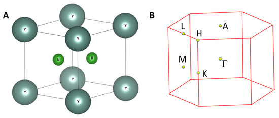
Figure 1.
(A) Structural model of P6/mmm YB2, (B) the bulk Brillouin zone (BZ) of YB2.
We used first principles to calculate the electronic structure of the entire YB2 material. For the exchange-correlation potential, the generalized gradient approximation (GGA) [46] of the Perdew–Burke–Ernzerhof (PBE) [47] function was adopted. In this study, the cutoff energy was set at 600 eV and the Brillouin zone was sampled using the Monkhorst–Pack k-point mesh with a size of 11 × 11 × 8. To determine the nontrivial surface states in YB2, the WANNIERTOOLS package (version 2.5.0) [48] was selected.
The crystal structure of YB2 was fully relaxed and the optimized lattice parameters were found to be a = b = 3.29 Å and c = 3.85 Å. These values are in a good agreement with the experimental ones [43]. Also, these values match well those in the Materials Project Database (a = b = 3.30 Å, c = 3.85 Å).
The Phonopy code was used to plot the phonon dispersion curve using the supercell-based approach. A 2 × 2 × 2 supercell was built and the phonon dispersion of the YB2 supercell along the Γ-M-K-Γ-A-L-H-A paths (see Figure 1B) is shown in Figure 2. The absence of imaginary frequencies in the first Brillouin zone confirms its dynamic stability.
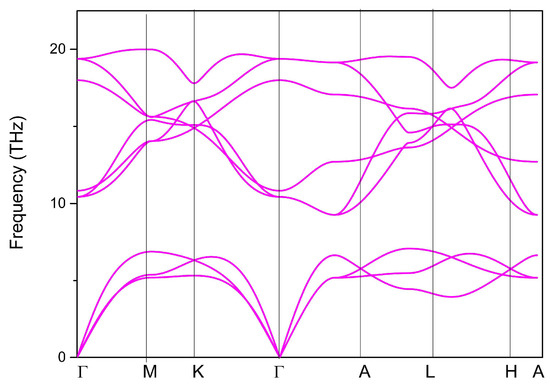
Figure 2.
Phonon dispersion curve of YB2.
3. Results and Discussion
Using the GGA–PBE method, the density of states of YB2 was produced and can be seen in Figure 3. We can see that this material exhibited metallic properties; however, the total density of states value was low, at around 2 eV. The total density of states in the range 0–2 eV was mainly dominated by Y-d orbitals (see the yellow area in Figure 3).
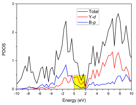
Figure 3.
The total and projected density of states (PDOSs) of YB2 without considering the spin–orbit coupling effect. The Fermi level energy is set at zero.
To fully understand the nontrivial band crossing points and the corresponding topological signatures, we also determined the band structure of YB2, as shown in Figure 4. From Figure 4, we can see two obvious band crossing points, named A1 and A2, near the K high symmetry points. Before discussing the topological signatures of both band crossing points, we should point out that the energy range of the linear band dispersion around the A1 and A2 band crossing points was more than 2 eV (see the yellow and green areas in Figure 4). Such a large linear energy range is substantially larger than most other proposed linear-type band dispersion materials [49]. Moreover, such a large linear energy range makes YB2 a promising candidate to study the physics related to experimental band crossings. To obtain an accurate range of the large linear band dispersion and band crossing points of YB2, the hybrid functional [50] was used to calculate the electronic structure along the M-K-Γ paths, and the results are shown in Figure 5. It is clear that the two band crossing points, A1 and A2, and the large range (larger than 2 eV) of the linear band dispersion were retained.
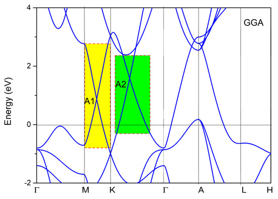
Figure 4.
Calculated band structure of YB2 without considering spin-orbit coupling (SOC.) The Fermi level energy is set at zero.
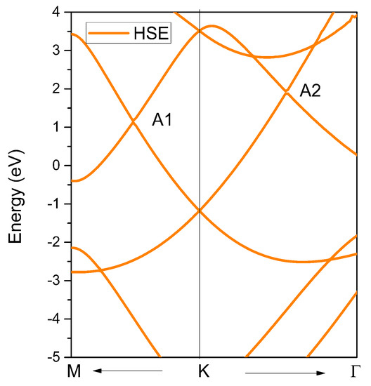
Figure 5.
The band structure of YB2 calculated using Heyd−Scuseria−Ernzerhof (HSE) 06.
Next, we discuss the topological signatures of these two band crossing points, A1 and A2, based on the arguments presented by Weng et al. [51]. These double-degenerated crossings should be assigned to a line, and the band crossing points should not be seen as isolated points. To further prove that A1 and A2 reside on a nodal line, the K-centered three-dimensional (3D) plot of the two bands in the kz = 0 plane as well as the K-centered 2D plot of the two bands in the kz = 0 plane are given in Figure 6A,B, respectively. The white lines in Figure 6 show the intersections between the two bands, namely, an obviously closed line. As shown in Figure 6A, we can see that the band crossing points belong to a nodal line in the kz = 0 plane, and this nodal line has a slight energy variation. The 2D plane figure of the K-centered nodal line is shown in Figure 6B.
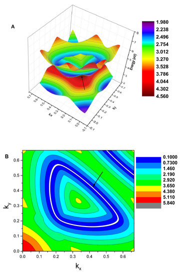
Figure 6.
(A) The 3D band dispersion around the K point in the kz = 0 plane. The white line shows the profile of the nodal line. (B) The 2D shape of the K-centered nodal line in the kz = 0 plane (highlighted by the white line and indicated using an arrow).
A YB2 crystal structure has two mechanisms to protect the nodal line: (1) A horizontal mirror plane with the nodal line located in the mirror-invariant kz = 0 plane and (2) inversion symmetry and time-reversal symmetry. It should be noted that the system has time-reversal symmetry and, thus, there should be the same nodal line centered at the K’ point, as shown in Figure 7. Note that the band structures of ScB2, VB2, ZrB2, NbB2, HfB2, and TaB2 with P6/mmm structure were calculated by Zhang et al. [52]. Based on their work, one can see that these above-mentioned materials also have large linear energy range.
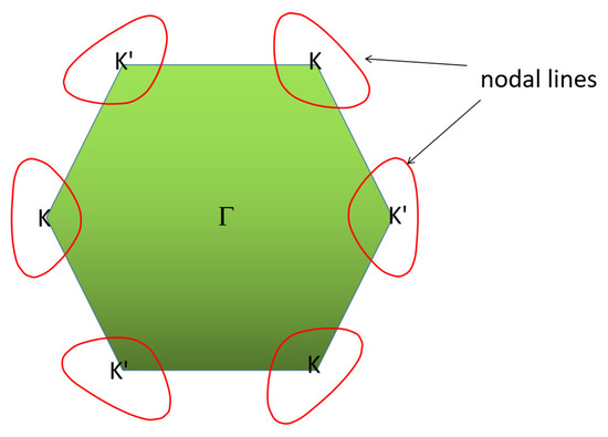
Figure 7.
Illustration of one pair of nodal lines (highlighted by red lines) in the kz = 0 plane.
The surface states along the (001) direction for the nodal line are given in Figure 8. In Figure 8B, the band crossing points are shown using yellow balls and the nontrivial surface states using red lines. From Figure 8B, one can see that the surface states along the path are merged in the bulk state; however, the surface states along the path are clearly defined. Note that the investigation of nodal line material is at initial stage, and some of them [53,54,55] have been confirmed in experiment. For example, the nodal line fermions of ZrSiSe [55] were proven in de Haas–van Alphen (dHvA) quantum oscillations.
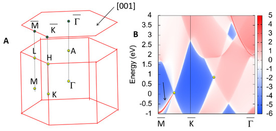
Figure 8.
(A) The 3D bulk of BZ and the 2D surface of BZ, (B) the projected spectrum of the (001) surface of YB2. The band crossing points and the nontrivial surface states are highlighted, using yellow balls and red lines, respectively.
The calculated electronic structures displayed above did not consider the spin–orbit coupling effect. Therefore, as a final consideration, we will discuss the effect of spin–orbit coupling on the band crossing points in the YB2 system. The results are shown in Figure 9; one can see that the spin–orbit coupling-induced gaps for points A1 and A2 were 31 meV and 40 meV, respectively. For almost all topological materials with nodal line states, gaps can be formed between their nodal lines via spin–orbit coupling effects. However, the spin–orbit coupling gaps in the YB2 system were relatively small in comparison to some well-known nodal line semimetals/metals, such as CaTe (~50 meV) [56], BaSn2 (>50 meV) [57], CaAgBi (>80 meV) [58], and TiOs (>100 meV) [59].
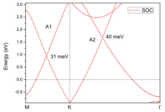
Figure 9.
The band structure of YB2 along the M-K-Γ paths calculated using GGA. The spin–orbit coupling effect is taken into consideration.
4. Conclusions
In conclusion, we have reported a perfect topological metal, P6/mmm-type YB2, using first principles. The P6/mmm-type YB2 has high structural stability, one pair of nodal lines in the kz = 0 plane, and a large linear energy range near the band crossings. The single pair of nodal lines are protected by two independent mechanisms: (1) Mirror symmetry and (2) inversion and time-reversal symmetries. We observed the nontrivial surface states in the (001) plane. Under the effect of spin–orbit coupling, gaps were present between the nodal lines with values of up to 40 meV. It should be noted that the spin–orbit coupling-induced gaps were smaller than some predicted nodal line state topological materials.
Author Contributions
Conceptualization, Y.L., M.K. and R.K.; Formal analysis, Y.L. and J.X.; Investigation, Y.L., M.K., J.X., and R.K.; Methodology, Y.L., M.K. and R.K.; Supervision, R.K., J.X., and K.M.; Writing—original draft, Y.L., M.K., and R.K. All authors have read and agreed to the published version of the manuscript.
Funding
This work was supported by the first batch of post-doctoral research fund projects in Yunnan Province (Serial No. 9), the Science and Technology Research Program of Chongqing Municipal Education Commission (Grant Nos. KJQN201801346 and KJ1711288), and the Chongqing University of Arts and Sciences Foundation (Grant No. Z2011Rcyj05). R. Khenata acknowledges the financial Support of the General Direction of Scientific Research and Technological Development (DGRSDT).
Conflicts of Interest
The authors declare no conflict of interest.
References
- Xue, H.; Yang, Y.; Gao, F.; Chong, Y.; Zhang, B. Acoustic higher-order topological insulator on a kagome lattice. Nat. Mater. 2018, 18, 108–112. [Google Scholar] [CrossRef] [PubMed]
- Yang, Y.; Gao, Z.; Xue, H.; Zhang, L.; He, M.; Yang, Z.; Singh, R.; Chong, Y.; Zhang, B.; Chen, H. Realization of a three-dimensional photonic topological insulator. Nature 2019, 565, 622–626. [Google Scholar] [CrossRef] [PubMed]
- Chen, Y.J.; Xu, L.X.; Li, J.H.; Li, Y.W.; Wang, H.; Zhang, C.F.; Li, H.; Wu, Y.; Liang, A.J.; Chen, C.; et al. Topological Electronic Structure and Its Temperature Evolution in Antiferromagnetic Topological Insulator MnBi2Te4. Phys. Rev. X 2019, 9, 041040. [Google Scholar] [CrossRef]
- Ni, X.; Li, M.; Weiner, M.; Alù, A.; Khanikaev, A.B. Demonstration of a quantized acoustic octupole topological insulator. Nat. Commun. 2020, 11, 1–7. [Google Scholar] [CrossRef]
- Harari, G.; Bandres, M.A.; Lumer, Y.; Rechtsman, M.C.; Chong, Y.; Khajavikhan, M.; Christodoulides, D.N.; Segev, M. Topological insulator laser: Theory. Science 2018, 359, eaar4003. [Google Scholar] [CrossRef]
- Bandres, M.A.; Wittek, S.; Harari, G.; Parto, M.; Ren, J.; Segev, M.; Christodoulides, D.N.; Khajavikhan, M. Topological insulator laser: Experiments. Science 2018, 359, eaar4005. [Google Scholar] [CrossRef]
- Klembt, S.; Harder, T.H.; Egorov, O.A.; Winkler, K.; Ge, R.; Bandres, M.A.; Emmerling, M.; Worschech, L.; Liew, T.C.H.; Segev, M.; et al. Exciton-polariton topological insulator. Nature 2018, 562, 552–556. [Google Scholar] [CrossRef]
- Franca, S.; Brink, J.V.D.; Fulga, I.C. An anomalous higher-order topological insulator. Phys. Rev. B 2018, 98, 201114. [Google Scholar] [CrossRef]
- He, C.; Ni, X.; Ge, H.; Sun, X.-C.; Chen, Y.-B.; Lu, M.-H.; Liu, X.-P.; Chen, Y.-F. Acoustic topological insulator and robust one-way sound transport. Nat. Phys. 2016, 12, 1124–1129. [Google Scholar] [CrossRef]
- Wang, Y.; Zhu, D.; Wu, Y.; Yang, Y.; Yu, J.; Ramaswamy, R.; Mishra, R.; Shi, S.; Elyasi, M.; Teo, K.-L.; et al. Room temperature magnetization switching in topological insulator-ferromagnet heterostructures by spin-orbit torques. Nat. Commun. 2017, 8, 1364. [Google Scholar] [CrossRef]
- Burkov, A.A. Topological semimetals. Nat. Mater. 2016, 15, 1145–1148. [Google Scholar] [CrossRef] [PubMed]
- Hu, J.; Xu, S.-Y.; Ni, N.; Mao, Z. Transport of Topological Semimetals. Annu. Rev. Mater. Res. 2019, 49, 207–252. [Google Scholar] [CrossRef]
- Gao, H.; Venderbos, J.W.; Kim, Y.; Rappe, A.M. Topological Semimetals from First Principles. Annu. Rev. Mater. Res. 2019, 49, 153–183. [Google Scholar] [CrossRef]
- Yang, T.; Zhang, X. Nearly flat nodal surface states in pseudo-one-dimensional molybdenum monochalcogenides X(MoS)3 (X = K, Rb, and Cs). J. Mater. Chem. C 2020, 8, 9046–9054. [Google Scholar] [CrossRef]
- Schoop, L.M.; Pielnhofer, F.; Lotsch, B.V. Chemical Principles of Topological Semimetals. Chem. Mater. 2018, 30, 3155–3176. [Google Scholar] [CrossRef]
- Bernevig, A.; Weng, H.; Fang, Z.; Dai, X. Recent Progress in the Study of Topological Semimetals. J. Phys. Soc. JPN 2018, 87, 041001. [Google Scholar] [CrossRef]
- Zhu, Z.; Winkler, G.W.; Wu, Q.; Li, J.; Soluyanov, A.A. Triple Point Topological Metals. Phys. Rev. X 2016, 6, 031003. [Google Scholar] [CrossRef]
- Burkov, A.A. Giant planar Hall effect in topological metals. Phys. Rev. B 2017, 96, 041110. [Google Scholar] [CrossRef]
- Ezawa, M. Non-Hermitian boundary and interface states in nonreciprocal higher-order topological metals and electrical circuits. Phys. Rev. B 2019, 99, 121411. [Google Scholar] [CrossRef]
- Ying, X.; Kamenev, A. Symmetry-Protected Topological Metals. Phys. Rev. Lett. 2018, 121, 086810. [Google Scholar] [CrossRef]
- Zhao, Y.X.; Wang, Z. Novel Z2 Topological Metals and Semimetals. Phys. Rev. Lett. 2016, 116, 016401. [Google Scholar] [CrossRef] [PubMed]
- Chang, G.; Xu, S.-Y.; Huang, S.-M.; Sanchez, D.S.; Hsu, C.-H.; Bian, G.; Yu, Z.-M.; Belopolski, I.; Alidoust, N.; Zheng, H.; et al. Nexus fermions in topological symmorphic crystalline metals. Sci. Rep. 2017, 7, 1688. [Google Scholar] [CrossRef] [PubMed]
- Huber, S.; Feldmeier, J.; Punk, M. Electron spectral functions in a quantum dimer model for topological metals. Phys. Rev. B 2018, 97, 075144. [Google Scholar] [CrossRef]
- Burkov, A.; Weyl, A. Metals. Annu. Rev. Condens. Matter Phys. 2018, 9, 359–378. [Google Scholar] [CrossRef]
- De Juan, F.; Zhang, Y.; Morimoto, T.; Sun, Y.; Moore, J.E.; Grushin, A.G. Difference frequency generation in topological semimetals. Phys. Rev. Res. 2020, 2, 012017. [Google Scholar] [CrossRef]
- Jin, L.; Zhang, X.; He, T.; Meng, W.; Dai, X.; Liu, G. Topological nodal line state in superconducting NaAlSi compound. J. Mater. Chem. C 2019, 7, 10694–10699. [Google Scholar] [CrossRef]
- He, T.; Zhang, X.; Meng, W.; Jin, L.; Dai, X.; Liu, G. Topological nodal lines and nodal points in the antiferromagnetic material β-Fe2PO5. J. Mater. Chem. C 2019, 7, 12657–12663. [Google Scholar] [CrossRef]
- Zhang, X.; Fu, B.; Jin, L.; Dai, X.; Liu, G.; Yao, Y. Topological Nodal Line Electrides: Realization of an Ideal Nodal Line State Nearly Immune from Spin–Orbit Coupling. J. Phys. Chem. C 2019, 123, 25871–25876. [Google Scholar] [CrossRef]
- Fang, C.; Weng, H.; Dai, X.; Fang, Z. Topological nodal line semimetals. Chin. Phys. B 2016, 25, 117106. [Google Scholar] [CrossRef]
- Jin, L.; Zhang, X.; Dai, X.F.; Wang, L.Y.; Liu, H.Y.; Liu, G. Screening topological materials with a CsCl-type structure in crystallographic databases. IUCrJ 2019, 6, 688–694. [Google Scholar] [CrossRef]
- Wang, X.; Ding, G.; Cheng, Z.; Wang, X.; Zhang, G.; Yang, T. Intersecting nodal rings in orthorhombic-type BaLi2Sn compound. J. Mater. Chem. C 2020, 8, 5461–5466. [Google Scholar] [CrossRef]
- Wang, X.; Cheng, Z.; Zhang, G.; Wang, B.; Wang, X.L.; Chen, H. Rich novel zero-dimensional (0D), 1D, and 2D topological elements predicted in the P63/m type ternary boride HfIr3B4. Nanoscale 2020, 12, 8314–8319. [Google Scholar] [CrossRef] [PubMed]
- Zhou, F.; Ding, G.; Cheng, Z.; Surucu, G.; Chen, H.; Wang, X. Pnma metal hydride system LiBH: A superior topological semimetal with the coexistence of twofold and quadruple degenerate topological nodal lines. J. Phys. Condens. Matter 2020, 32, 365502. [Google Scholar] [CrossRef] [PubMed]
- Nie, S.; Weng, H.; Prinz, F.B. Topological nodal-line semimetals in ferromagnetic rare-earth-metal monohalides. Phys. Rev. B 2019, 99, 035125. [Google Scholar] [CrossRef]
- Geng, Z.-G.; Peng, Y.-G.; Shen, Y.-X.; Ma, Z.; Yu, R.; Gao, J.-H.; Zhu, X. Topological nodal line states in three-dimensional ball-and-stick sonic crystals. Phys. Rev. B 2019, 100, 224105. [Google Scholar] [CrossRef]
- Xiao, M.; Sun, X.-Q.; Fan, S. Nodal chain semimetal in geometrically frustrated systems. Phys. Rev. B 2019, 99, 094206. [Google Scholar] [CrossRef]
- Zhang, R.-W.; Zhang, Z.; Liu, C.-C.; Yao, Y. Nodal Line Spin-Gapless Semimetals and High-Quality Candidate Materials. Phys. Rev. Lett. 2020, 124, 016402. [Google Scholar] [CrossRef]
- Lu, J.; Huang, X.; Yan, M.; Li, F.; Deng, W.; Liu, Z. Nodal-Chain Semimetal States and Topological Focusing in Phononic Crystals. Phys. Rev. Appl. 2020, 13, 054080. [Google Scholar] [CrossRef]
- Wang, J.-T.; Nie, S.; Weng, H.; Kawazoe, Y.; Chen, C. Topological Nodal-Net Semimetal in a Graphene Network Structure. Phys. Rev. Lett. 2018, 120, 026402. [Google Scholar] [CrossRef]
- Yan, Z.; Bi, R.; Shen, H.; Lu, L.; Zhang, S.-C.; Wang, Z. Nodal-link semimetals. Phys. Rev. B 2017, 96, 041103. [Google Scholar] [CrossRef]
- Liu, Z.; Lou, R.; Guo, P.; Wang, Q.; Sun, S.; Li, C.; Thirupathaiah, S.; Fedorov, A.; Shen, D.; Liu, K.; et al. Experimental Observation of Dirac Nodal Links in Centrosymmetric Semimetal TiB2. Phys. Rev. X 2018, 8, 031044. [Google Scholar] [CrossRef]
- Chen, W.; Lu, H.-Z.; Hou, J.-M. Topological semimetals with a double-helix nodal link. Phys. Rev. B 2017, 96, 041102. [Google Scholar] [CrossRef]
- Klesnar, H.P.; Rogl, P. Phase relations in the ternary systems rare-earth metal (RE)-boron-nitrogen, where RE = Tb, Dy, Ho, Er, Tm, Lu, Sc, and Y. High Temperatures. High Press. 1990, 22, 453–457. [Google Scholar]
- Song, J.M.; Liu, H.; Pang, Y. Research on YB2 Powder Preparation by Solid State Reaction. Rare Met. Cement. Carbides 2015, 45, 12–15. [Google Scholar]
- Available online: https://materialsproject.org/materials/mp-1542/ (accessed on 28 June 2020).
- Perdew, J.P.; Burke, K.; Ernzerhof, M. Generalized Gradient Approximation Made Simple. Phys. Rev. Lett. 1996, 77, 3865–3868. [Google Scholar] [CrossRef]
- Perdew, J.P.; Burke, K.; Ernzerhof, M. Perdew, Burke, and Ernzerhof Reply. Phys. Rev. Lett. 1998, 80, 891. [Google Scholar] [CrossRef]
- Wu, Q.; Zhang, S.; Song, H.-F.; Troyer, M.; Soluyanov, A.A. WannierTools: An open-source software package for novel topological materials. Comput. Phys. Commun. 2018, 224, 405–416. [Google Scholar] [CrossRef]
- Wang, X.; Li, T.; Cheng, Z.; Wang, X.-L.; Chen, H. Recent advances in Dirac spin-gapless semiconductors. Appl. Phys. Rev. 2018, 5, 041103. [Google Scholar] [CrossRef]
- Deák, P.; Aradi, B.; Frauenheim, T.; Janzén, E.; Gali, A. Accurate defect levels obtained from the HSE06 range-separated hybrid functional. Phys. Rev. B 2010, 81, 153203. [Google Scholar] [CrossRef]
- Weng, H.; Liang, Y.; Xu, Q.; Yu, R.; Fang, Z.; Dai, X.; Kawazoe, Y. Topological node-line semimetal in three-dimensional graphene networks. Phys. Rev. B 2015, 92, 045108. [Google Scholar] [CrossRef]
- Zhang, X.; Yu, Z.-M.; Sheng, X.-L.; Yang, H.Y.; Yang, S.A. Coexistence of four-band nodal rings and triply degenerate nodal points in centrosymmetric metal diborides. Phys. Rev. B 2017, 95, 235116. [Google Scholar] [CrossRef]
- Bian, G.; Chang, T.-R.; Sankar, R.; Xu, S.-Y.; Zheng, H.; Neupert, T.; Chiu, C.-K.; Huang, S.-M.; Chang, G.; Belopolski, I.; et al. Topological nodal-line fermions in spin-orbit metal PbTaSe2. Nat. Commun. 2016, 7, 10556. [Google Scholar] [CrossRef] [PubMed]
- Wu, Y.; Wang, L.-L.; Mun, E.; Johnson, D.D.; Mou, D.; Huang, L.; Lee, Y.; Bud’Ko, S.L.; Canfield, P.C.; Kaminski, A. Dirac node arcs in PtSn4. Nat. Phys. 2016, 12, 667–671. [Google Scholar] [CrossRef]
- Hu, J.; Tang, Z.; Liu, J.; Zhu, Y.; Graf, D.; Myhro, K.; Tran, S.; Lau, C.N.; Wei, J.; Mao, Z.Q. Evidence of Topological Nodal-Line Fermions in ZrSiSe and ZrSiTe. Phys. Rev. Lett. 2016, 117, 016602. [Google Scholar] [CrossRef] [PubMed]
- Du, Y.; Tang, F.; Wang, D.; Sheng, L.; Kan, E.; Duan, C.; Savrasov, S.Y.; Wan, X. CaTe: A new topological node-line and Dirac semimetal. NPJ Quant. Mater. 2017, 2, 1–4. [Google Scholar] [CrossRef]
- Huang, H.; Liu, J.; Vanderbilt, D.; Duan, W. Topological nodal-line semimetals in alkaline-earth stannides, germanides, and silicides. Phys. Rev. B 2016, 93, 201114. [Google Scholar] [CrossRef]
- Yamakage, A.; Yamakawa, Y.; Tanaka, Y.; Okamoto, Y. Line-Node Dirac Semimetal and Topological Insulating Phase in Noncentrosymmetric Pnictides CaAgX(X = P, As). J. Phys. Soc. JPN 2016, 85, 013708. [Google Scholar] [CrossRef]
- Wang, X.; Ding, G.; Cheng, Z.; Surucu, G.; Wang, X.-L.; Ding, G. Novel topological nodal lines and exotic drum-head-like surface states in synthesized CsCl-type binary alloy TiOs. J. Adv. Res. 2020, 22, 137–144. [Google Scholar] [CrossRef]
© 2020 by the authors. Licensee MDPI, Basel, Switzerland. This article is an open access article distributed under the terms and conditions of the Creative Commons Attribution (CC BY) license (http://creativecommons.org/licenses/by/4.0/).