Abstract
The DC converter constitutes a pivotal component within medium-voltage direct current (MVDC) collection systems, performing functions such as voltage boosting, isolation, and power transmission. To accommodate the demand for high-capacity DC converters in MVDC collection systems for new energy sources, a full-bridge medium-frequency converter featuring low voltage and current stress on auxiliary switching devices is proposed. Based on the principles of dual-transformer configuration and component sharing, this converter employs a half-bridge circuit and a full-bridge circuit sharing two switching devices. Utilizing mixed-frequency modulation, the full-bridge main circuit operates at medium frequency to transmit the majority of power, while the half-bridge auxiliary circuit regulates overall power and voltage through high-frequency chopping control. This achieves zero-current switching for the medium-frequency switching devices across the entire load range, significantly reducing switching losses in the converter. This paper details the converter’s operating principles and analyzes key parameter design methodologies. Finally, a 240–6000 V/7200 W prototype was constructed to validate the proposed converter’s performance.
1. Introduction
With the escalating severity of issues such as the energy crisis, the greenhouse effect, and environmental pollution, new energy sources have garnered widespread global attention and seen increasingly extensive application. According to the China Power Industry Annual Development Report 2023 [1], China’s electrification process is projected to enter a mid-term transition phase by 2030, accelerating the pace of green and low-carbon transformation in the power sector. Non-fossil energy sources will account for approximately 60% of installed power generation capacity, contribute nearly 50% of total electricity generation, and provide around 90% of the incremental electricity demand growth across society. As renewable energy generation capacity continues to expand both domestically and globally, technologies for aggregating and transmitting this energy have garnered significant attention. The adoption of Medium-Voltage Direct Current (MVDC) collection for renewable energy generation represents a significant future development direction [2]. As early as 2016, China’s National Key R&D Program for Smart Grids established a dedicated project titled ‘Research and Development of Key Technologies and Equipment for DC Step-Up Collection and Grid Integration of Large-Scale Photovoltaic Power Stations’ within its inaugural batch of initiatives [2,3].
The core equipment for MVDC collection systems in renewable energy generation is the high-power, high-voltage-ratio DC converter, which elevates the DC from the renewable energy side to the medium-voltage DC level. In high-power applications, IGBTs serve as the primary power devices. Achieving Zero Current Switching (ZCS) in IGBTs is crucial for reducing switching losses, enhancing efficiency, and enabling more effective utilization of renewable energy [4]. Parameters such as the converter’s input voltage, output voltage, and rated transmission power influence the selection of its fundamental topology, which in turn affects the realization of soft switching in power semiconductor devices [5]. Researchers worldwide have conducted extensive studies on DC boost converters, including LC resonant converters [6,7,8]. Reference [9] comprehensively considered semiconductor device selection and arrangement, resonant capacitor selection and structural layout, and high-power high-frequency transformer design. It theoretically designed a novel LC series resonant full-bridge converter and conducted loss assessments, predicting efficiencies exceeding 98.5%.
To reduce voltage stress on switching devices, multilevel circuits may be employed [10,11]. In commonly used three-level circuits [12,13,14], the voltage stress on switching devices is only half the input voltage.
The authors in [15] proposed a dual full-bridge converter based on a dual-transformer structure. This comprises a main circuit and an auxiliary circuit. By designing the transformer turns ratio, the main circuit transmits the majority of the power. The main circuit operates in open-loop mode, whilst closed-loop control of the auxiliary circuit regulates the converter’s voltage and power. This approach simplifies control and facilitates ZCS implementation. However, the dual full-bridge configuration increases the number of switching devices and introduces insulation challenges for the high-voltage-side inductors.
The author’s work in references [16,17,18,19,20] proposes a multiplexed bridge arm combination ZCS full-bridge converter. Based on the principle of device multiplexing [21,22,23], by combining two full-bridge circuits to reduce two switches. This achieves zero-current turn-on and turn-off for the main circuit’s four switches, whilst the two auxiliary switches enable zero-voltage turn-on and turn-off. It also eliminates the high-voltage-side filter inductor, resolving insulation concerns associated with high-voltage inductors. However, during the auxiliary circuit’s mid-voltage-side freewheeling period, it does not transfer energy to the secondary side. This increases unnecessary switch conduction losses and reduces converter efficiency.
In summary, DC/DC converters within new energy MVDC collection systems require substantial capacity. However, high-frequency (typically referring to frequencies significantly higher than line frequency, such as several tens of kHz and above) DC/DC converters struggle to achieve large capacities, necessitating multiple modules in parallel—a solution that incurs higher costs.
This paper proposes a full-bridge medium-frequency converter with low voltage and current stress on auxiliary switching devices. Employing a medium-high frequency hybrid modulation technique, the current waveform approximates a discontinuous trapezoidal wave, significantly reducing current stress on switching components. Furthermore, the transformer operates at a medium frequency of 500 Hz, facilitating the design and manufacture of higher power ratings. Based on dual-transformer and component-sharing principles, power and voltage regulation across the entire converter is achieved by adjusting the duty cycle of the high-frequency switching transistor. Zero-current switching (ZCS) is realized during both turn-on and turn-off across the full load range, whilst the four main circuit switching transistors operate in a fixed duty cycle mode, offering the advantage of simplified control. By designing the main transformer’s step-up ratio such that the main circuit handles the majority of power transfer while the auxiliary circuit manages a minor portion, the current flowing through the high-frequency switching transistors is reduced. This significantly lowers the switching losses within the converter.
2. Transformer Topology and Working Principle
As shown in Figure 1, the proposed full-bridge medium-frequency converter topology features low voltage and current stress on auxiliary switching devices. Transistors Q1 to Q4, transformer Tr1, and its leakage inductance Lt1 form a full-bridge main circuit. The voltage-dividing capacitors Cin1 and Cin2, freewheeling diodes Dc1 and Dc2, switch transistors Q1, Q2, Q5, and Q6, transformer Tr2 and its leakage inductance Lt2 form an auxiliary half-bridge circuit. Switching transistors Q1 and Q2 serve as common switches for both the main circuit and auxiliary branch. The output side comprises a rectifier circuit, with the secondary windings of Tr1 and Tr2 directly connected in series to form its input.
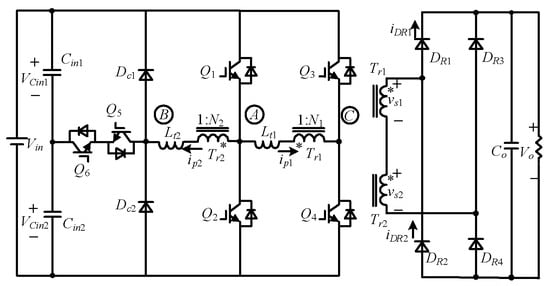
Figure 1.
Topology of full-bridge converter with low voltage and current stress.
Figure 2 shows the main operating waveforms of the proposed full-bridge medium-frequency converter with low voltage and current stress on the auxiliary switches. Auxiliary switches Q5 and Q6 employ PWM chopping control and operate in high-frequency mode, while Q1, Q2, Q3, and Q4 operate at 500 Hz. To achieve ZCS, they are driven with a fixed 50% duty cycle rather than PWM control. Q1 and Q4 turn on and off simultaneously, while Q2 and Q3 turn on and off together. Consequently, the main power circuit operates in an open-loop state, with the entire converter achieving port voltage and power transfer control through the chopping of auxiliary switches Q5 and Q6.
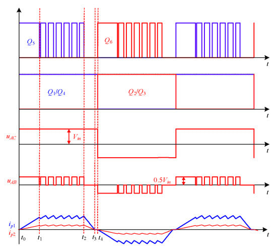
Figure 2.
Typical working waveform.
Before detailed analysis, the following assumptions are made:
- All switches, diodes, inductors, and capacitors are ideal components.
- The input voltage-dividing capacitors Cin1 and Cin2 are equal and sufficiently large, so VCin1 = VCin2 = Vin/2; capacitors Cin1 and Cin2 are equal and sufficiently large.
- The leakage inductance of transformer Tr2 is sufficiently small and negligible.
As shown in Figure 2, this converter exhibits four distinct modes within half a medium-frequency switching cycle. These are Mode 1 [t0–t1], Mode 2 [t1–t2], Mode 3 [t2–t3], and Mode 4 [t3–t4]. Mode 1 [t0, t1]: The current path for this mode is shown in Figure 3a. Since no current flows through any switching transistors before time t0, Q1, Q4, and Q5 achieve ZCS turn-on. At this point, the main circuit portion forms a loop consisting of Vin, Q1, Lt1, Tr1, and Q4. The auxiliary branch forms a loop with Vin, Q1, Lt2, Tr2, Q5, and the reverse-parallel diodes of Q6. The current flowing through switch Q1 is the sum of the currents in both loops. The equivalent circuit of this mode converted to the secondary side is shown in Figure 4a. In this mode, the voltage between points A and B is Vin/2. Therefore, the voltage across the secondary winding of auxiliary transformer Tr2 auxiliary winding voltage is N2Vin/2, the Tr1 auxiliary winding voltage is Vo − N2Vin/2, and the voltage across the leakage inductance Lt1 is
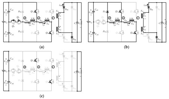
Figure 3.
Current flow diagram. (a) Current rise; (b) Current drop; (c) Zero current.
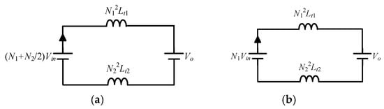
Figure 4.
Equivalent circuit. (a) Current rise; (b) Current drop.
The currents flowing into the main transformer and auxiliary transformer, ip1 and ip2, respectively, are
For the current in this mode to rise to its steady-state value, vLt1 > 0 must be satisfied, yielding
Mode 2 [t1, t2]: This mode employs high-frequency chopping via switching transistor Q5 to oscillate the current near its steady-state value. When high-frequency switching transistor Q5 is turned on, the current increases linearly, with the current path as shown in Figure 3a. When high-frequency switching transistor Q5 is turned off, the current decreases linearly. At this time, the current path in the auxiliary branch consists of DC1, Q1, Lt2, and Tr2, while the current path in the main circuit remains unchanged, as shown in Figure 3b. The current flowing through switch Q8 remains the sum of the two loops. When high-frequency switch Q5 turns off, the voltage between points A and B equals zero. The equivalent circuit on the secondary side, as shown in Figure 4b, indicates that the voltage across the secondary winding of auxiliary transformer Tr2 is also zero. Therefore, the voltage across the secondary winding of Tr1 equals Vo, and the voltage across the leakage inductor Lt1 is
To allow the current to fluctuate near its steady-state value, it is necessary to satisfy vLt1 < 0, from which we obtain
Mode 3 [t2, t3]: The current path for this mode is shown in Figure 3b. At time t2, switch Q5 turns off, causing the current to decrease linearly. By time t3, the current drops to zero. The secondary-side rectifier diodes DR1 and DR4 naturally turn off. This mode operates identically to Mode 2 when the high-frequency switch Q5 turns off.
Mode 4 [t3, t4]: The current flow diagram for this mode is shown in Figure 3c. Although the medium-frequency switching transistors Q1 and Q4 are in the on state, the inductor current remains zero throughout. Time t4 marks the end of the upper switching cycle and the start of the lower switching cycle. At t4, Q1 and Q4 achieve ZCS turn-off. After a fixed dead time, Q2, Q3, and Q6 achieve ZCS turn-on due to the transformer leakage inductance suppressing rapid current rise.
3. Parameter Design
This section presents parameter design using the following operating parameters: input voltage Vin = 1500 V, output voltage Vo = 20 kV, rated power PN = 500 kW, medium-frequency switching frequency fM = 500 Hz, and high-frequency switching frequency fH = 10 kHz.
- (a)
- Main Transformer Turns Ratio N1
Assuming no losses during power transmission, the total power transmitted by the converter during the upper half-cycle is obtained from Figure 3 as
Similarly, the power transmitted by the main circuit is
From Equations (6) and (7), the ratio of the power transmitted by the main circuit to the total power is
From Equation (8), it can be seen that the proportion of power transmitted by the main circuit is proportional to the main transformer’s turns ratio N1. That is, the larger N1 is, the more power is transmitted by the main circuit. Since the switching transistors in the main circuit can achieve ZCS turn-off, it is desirable for the main circuit to transmit a larger proportion of power. Setting Pm:Ptot = 0.9 yields the condition required for the main circuit to transmit 90% of the power:
- (b)
- Auxiliary transformer turns ratio N2
From Equations (3) and (9), we obtain
Solving the above equation yields the range for N2:
Referring to Figure 2, applying the volt-second balance principle to the leakage inductance Lt1 of the main transformer during modes 1 and 3 yields
where ton denotes the time interval from t0 to t1, and toff denotes the time interval from t2 to t3.
From Equation (12), we obtain
Based on Equation (13), the total power transmitted by the converter during the upper half-cycle is expressed as
Neglecting the auxiliary transformer leakage inductance Lt2, Equation (14) simplifies to
Solving Equation (15) yields the relationship between the rise time ton and the auxiliary transformer turns ratio N2 and the main transformer leakage inductance Lt1
where
According to Equations (2) and (16), the steady-state values of the current ip1 flowing into the main transformer and the current ip2 flowing into the auxiliary transformer are
Equation (18) enables plotting the variation curves of Ip1 and Ip2 with respect to the auxiliary transformer turns ratio N2 and the main transformer leakage inductance Lt1, as shown in Figure 5 and Figure 6.
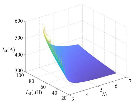
Figure 5.
The curve of Ip1 with N2 and Lt1.
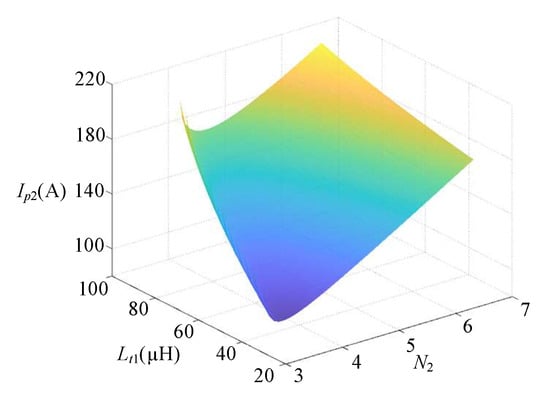
Figure 6.
The curve of Ip2 with N2 and Lt1.
As shown in Figure 5, when N2 < 4, the steady-state value of the current flowing into the main transformer, Ip1, decreases rapidly with increasing N2. When N2 > 4, the trend of Ip1 decreases more gradually as N2 increases. The primary loss source in the power devices of the converter proposed in this paper is the conduction loss of the intermediate frequency switching transistor. Therefore, to reduce the overall loss of the converter, it is necessary to minimize the conduction loss of the intermediate frequency switching transistor. This requires the steady-state current flowing into the main transformer, Ip1, to be as small as possible. Consequently, the turns ratio N2 of the auxiliary transformer should be set to a larger value. However, as shown in Figure 6, the steady-state current Ip2 flowing into the auxiliary transformer increases rapidly with the increase in the auxiliary transformer turns ratio N2. This leads to a rapid increase in the switching losses of the high-frequency switching transistor. Therefore, N2 cannot be set too large. After comprehensive consideration, N2 = 4 is selected.
- (c)
- For the leakage inductance Lt1 of the main transformer
Applying the volt-second balance principle to both ends of the inductance Lt1 in Mode 2 yields
Solving Equation (19) yields the duty cycle D of the high-frequency switching transistor in mode 2 as
From this, the current ripple ΔIp during the plateau phase can be calculated. The relationship between Vin and L is given by
According to Equations (18) and (21), the peak currents of ip1 and ip2 are obtained as
Based on the converter’s operating principle, the sum of ip1_peak and ip2_peak represents the peak current flowing through the common switch transistor Q1. According to Equation (22), the peak currents ip1, ip2 and the peak current iQ1_peak flowing through the common switch transistor Q1 relative to the leakage inductance Lt1 as shown in Figure 7.
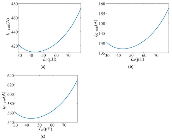
Figure 7.
The curve of partial current peak with Lt1. (a) The relationship curve between ip1_peak and Lt1.; (b) the relationship curve between ip2_peak and Lt1; (c) the relationship curve between iQ1_peak and Lt1.
It can be seen that ip1_peak and ip2_peak and the peak current iQ1_peak flowing through the common switch transistor Q1, all exhibit a consistent trend with the variation in the main transformer leakage inductance Lt1. They initially decrease and then increase as Lt1 increases, reaching a minimum at Lt1 = 43 µH. Since ip1_peak and iQ1_peak increase, the conduction losses of the medium-frequency switch transistor also increase, which is unfavorable for its selection. Similarly, the larger ip2_peak becomes, the greater the switching losses of the high-frequency switch transistor. Therefore, it is desirable for all three values to be as small as possible. Hence, Lt1 = 43 µH is selected.
- (d)
- Selection of Light-Load Switching Power Ps
When the transmitted power decreases, the converter’s current waveform reduces overall. Based on ip1(t1) = ΔIp1/2, the critical continuous power is obtained as
When the converter’s transmitted power is less than or equal to Ps, the operating frequency of the high-frequency switching transistor is also reduced to 500 Hz.
4. Simulation Verification
Based on the results of the parameter design, the converter parameters are obtained as shown in Table 1. To verify the working principle of the proposed converter, its circuit model and thermal simulation model were constructed in PLECS.

Table 1.
Simulation Parameters.
Figure 8 shows steady-state simulation waveforms under (a) full-load conditions and (b) light-load conditions (15% PN). The simulation waveforms align with theoretical waveforms.
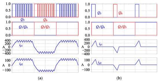
Figure 8.
Steady-state simulation waveform of each working condition. (a) Full load; (b) light load.
To verify the soft-switching characteristics of the intermediate frequency switching devices, Figure 9 presents the drive voltages and current waveforms for the main circuit switching devices Q3 and Q4 as well as the common switching device Q1 and Q2 under full load (100% PN) and light load (15% PN) conditions. Before each intermediate frequency switch turns off, the current flowing through it decreases to zero, achieving ZCS turn-off. Before each intermediate frequency switch turns on, the current flowing through it remains zero, and the current rises slowly upon turn-on, achieving ZCS turn-on.
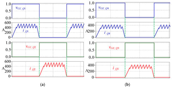
Figure 9.
If switch device soft switching waveform. (a) Common switch transistor; (b) main circuit switch transistor.
Based on the simulation results, Table 2 presents the peak and RMS current values flowing into each switching device. Since the main circuit undertakes 90% of the power transfer, the conduction current of each switching device in the main circuit is significantly higher than that of the switching devices in the auxiliary circuit.
Table 2.
Current through each power device (A).
To provide a detailed comparison of the loss characteristics of the power devices, device selection and thermal simulations were performed for this converter. For the high-frequency chopping switch, the IKQ120N120CS7 IGBT (Infineon Technologies AG, Neubiberg, Germany)was selected. This IGBT has a maximum RMS current rating of 144 A (@Tc = 100 °C), and its anti-parallel diode is rated for a maximum RMS current of 125 A (@Tc = 100 °C). Therefore, the diodes Dc1 and Dc2 can directly utilize the anti-parallel diode of this IGBT. For the common switch and the main circuit switches, the FF450R33T3E3 (1200 V/450 A, Infineon Technologies AG, Neubiberg, Germany) was chosen.
By setting the junction temperature of the power devices at a stable 100 °C, the simulated loss results are summarized in Table 3. As can be seen, Q1/Q2 and Q3/Q4 operate with zero-current switching (ZCS), resulting in negligible switching losses. Although Q5/Q6 and Dc1/Dc2 are hard-switched, the current flowing through them is relatively small, so their switching losses account for a low proportion—only 9.7% of the total device losses.
Table 3.
Simulation Results of Converter Losses (A).
5. Experimental Verification
Based on the above theoretical analysis, a low-power experimental platform was constructed to further validate the proposed converter’s operating principles and performance, as depicted in Figure 10. Key parameters are shown in Table 4.
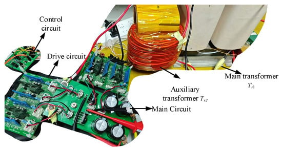
Figure 10.
Experimental prototype.
Table 4.
Experimental Parameters.
Figure 11 shows the drive signal vGE_Q1 for the shared switch transistor Q1 under full load (7.2 kW), half load (3.6 kW), and light load (1150 W) conditions, the drive voltage vGE_Q5 for the high-frequency chopping switch Q5, the current ip1 flowing through the main transformer, and the current ip2 flowing through the auxiliary transformer. Comparing the waveforms of ip1 and ip2 under various operating conditions reveals that the peak value of ip2 is significantly smaller than that of ip1. This indicates that the currents during hard switching and turn-on of the high-frequency chopping switch Q5 are very small, resulting in minimal switching losses.
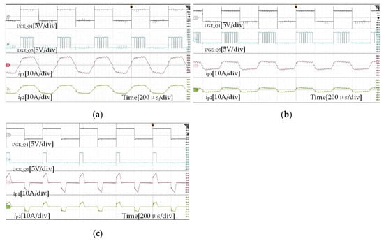
Figure 11.
Steady state waveform under each working condition. (a) full load; (b) half load; (c) light load.
The current flowing through the shared switches Q1 and Q2 is the sum of the two branch currents. The current flowing through the main circuit switches Q3 and Q4 is the main transformer current ip1. Figure 12 shows the terminal voltage vQ1 to vQ4 and the current waveforms flowing through them under full-load conditions. Observing that ip1 and ip2 are zero at the switch turn-off instant demonstrates that Q1 to Q4 achieve ZCS turn-off.
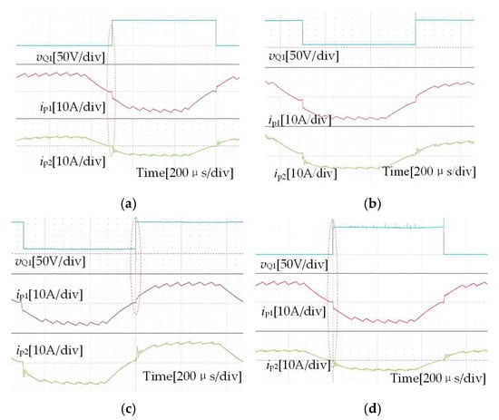
Figure 12.
Waveforms of vQ and current of ip under full load condition. (a) Q1; (b) Q2; (c) Q3; (d) Q4.
Figure 13 shows the terminal voltages vQ1 to vQ2 of switching transistors Q1 to Q4 under light load conditions for the current waveforms and the corresponding current waveforms. Observing that ip1 and ip2 drop to zero at the switch turn-off instant demonstrates that ZCS turn-off is also achievable for Q1~Q4 under light load conditions.
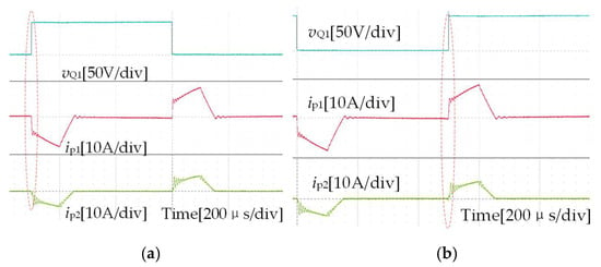
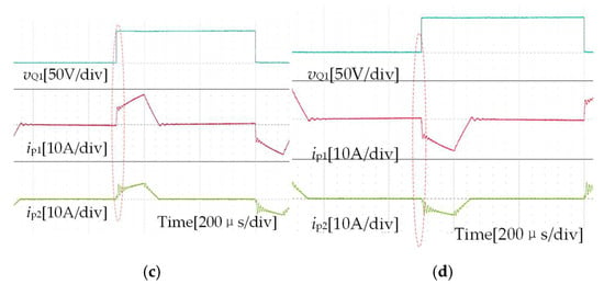
Figure 13.
Waveforms of vQ and current of ip under light load condition. (a) Q1; (b) Q2; (c) Q3; (d) Q4.
Regarding the efficiency characteristics of the proposed converter, prototype efficiency was tested at different output powers. Figure 14 shows the efficiency curves of the converter at various output powers. It can be seen that due to the introduction of an auxiliary branch for small-current high-frequency chopping, combined with the main circuit switches operating in ZCS mode, actual switching losses are minimal. Efficiency exceeds 97% across a wide power range.
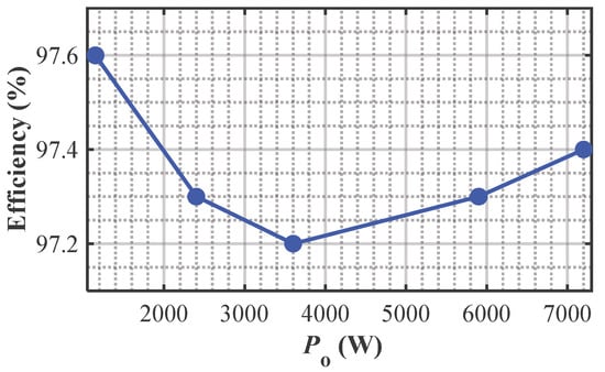
Figure 14.
Converter efficiency.
6. Conclusions
This paper proposes a full-bridge medium-frequency converter based on mixed-frequency modulation, featuring low voltage and current stress on the auxiliary switches. The main work involves integrating a dual-transformer structure and component reuse to construct a main circuit and an auxiliary branch consisting of four medium-frequency switches, two high-frequency switches, and two shared medium-frequency switches.
The key contributions of this scheme are reflected in the following aspects: First, power and voltage regulation of the entire converter is achieved solely by adjusting the duty cycle of the chopper control for the two high-frequency switches in the auxiliary branch. This allows all medium-frequency switches to operate in a fixed duty cycle mode, thereby simplifying the control system. Second, this modulation method enables zero-current switching for both turn-on and turn-off of the medium-frequency switches, effectively reducing switching losses. Furthermore, by rationally designing the turns ratio of the main transformer, the majority of power is transmitted through the main circuit. The auxiliary transformer is designed with a smaller step-up ratio and is responsible for transmitting only a small portion of the power, which helps reduce the peak current of the switches and further improves efficiency.
Finally, experimental studies validate the feasibility and excellent performance of the proposed converter, confirming the correctness of the above theoretical analysis.
Author Contributions
Methodology, S.G.; Software, C.L.; Validation, W.C.; Formal analysis, H.Z. All authors have read and agreed to the published version of the manuscript.
Funding
This work was supported in part by Supported by Liaoning Province Science and Technology Plan Project (2023JH1/10400075).
Data Availability Statement
The original contributions presented in this study are included in the article. Further inquiries can be directed to the corresponding author.
Conflicts of Interest
Author Shilong Gao was employed by the company State Grid Economic and Technological Research Institute Co., Ltd. The remaining authors declare that the research was conducted in the absence of any commercial or financial relationships that could be construed as a potential conflict of interest.
References
- China Electricity Council (CEC). China Electricity Council Releases Annual Development Report on China’s Power Industry 2023. China Electric Power News, 12 July 2023. (In Chinese) [Google Scholar]
- Jiang, D.; Gu, H.; Yin, R.; Chen, K.; Liang, Y.; Wang, Y. Research status and development prospect of offshore DC Wind Farm. Grid Technol. 2015, 39, 2424–2431. (In Chinese) [Google Scholar]
- Song, Q.; Zhao, B.; Liu, W.H.; Zeng, R. Review of intelligent DC distribution networks. Chin. J. Electr. Eng. 2013, 33, 9–19. (In Chinese) [Google Scholar]
- Ivensky, G.; Zeltser, I.; Kats, A.; Ben-Yaakov, S. Reducing IGBT losses in ZCS series resonant converters. In IEEE Proceedings of the Applied Power Electronics Conference; IEEE: New York City, NY, USA, 1996. [Google Scholar]
- Pan, Z.; Ning, G.; Yuan, D.; Fu, H.; Sui, S.; Azeem, S.W. Hybrid resonant three-level zero-current switching converter based on two transformers. Power Syst. Autom. 2019, 43, 135–143. (In Chinese) [Google Scholar]
- Chen, W.; Huang, A.; Li, C.; Wang, G. A high efficiency high power step-up resonant switched-capacitor converter for offshore wind energy systems. In IEEE Proceedings of the Energy Conversion Congress and Exposition (ECCE); IEEE: Raleigh, NC, USA, 2012. [Google Scholar]
- Wu, S.; Liu, W.; Ji, L.; Li, J. Research on data flow fault tolerance of new energy power generation forecasting system. Electr. Eng. 2018, 19, 107–111. (In Chinese) [Google Scholar]
- Yin, Z.; Hu, J.; Chung, H.S.; Ioinovici, A. A ZCS-PWM voltage-driven three-level converter with a secondary-side simple soft-switching snubber. IEEE Trans. Ind. Electron. 2016, 63, 7542–7552. [Google Scholar] [CrossRef]
- Dincan, C.G.; Kjaer, P.; Chen, Y.H.; Sarrá-Macia, E.; Munk-Nielsen, S.; Bak, C.L.; Vaisambhayana, S. Design of a High-Power Resonant Converter for DC Wind Turbines. IEEE Trans. Power Electron. 2019, 34, 6136–6154. [Google Scholar] [CrossRef]
- Ortiz, G.; Leibl, M.G.; Huber, J.E.; Kolar, J.W. Design and experimental testing of a resonant DC-DC converter for solid-state transformers. IEEE Trans. Power Electron. 2017, 32, 7534–7542. [Google Scholar] [CrossRef]
- Cao, G.; Guo, Z.; Wang, Y.; Sun, K.; Kim, H.-J. A DC-DC conversion system for high power HVDC connected photovoltaic power system. In Proceedings of the 20th International Conference on Electrical Machines and Systems (ICEMS), Sydney, NSW, Australia, 11–14 August 2017. [Google Scholar]
- Wang, Y.; Han, F.; Yang, L.; Wang, C.; Zhou, B. A dual transformer-structured multi-resonant soft-switching DC-DC converter. Trans. China Electrotech. Soc. 2019, 34, 738–746. (In Chinese) [Google Scholar]
- Li, F.; Deng, H.; Zhang, G.; Pei, W.; Deng, W. A cascaded bidirectional DC-DC converter with intermediate capacitor resonance. Trans. China Electrotech. Soc. 2022, 37, 5253–5266. (In Chinese) [Google Scholar]
- Sun, T.; Gao, T.; Qu, H.; Zhou, Y. A ZVS three-level DC-DC converter with auxiliary transformer. Proc. CSEE. 2011, 31, 28–33. (In Chinese) [Google Scholar]
- Peng, Y.; Xue, B.; Wang, L.; Wang, H. An Active Voltage Quadrupler Rectifier Based Multidirectional Three-Port Converter in 800V Micro-Grids. In Proceedings of the IEEE Applied Power Electronics Conference and Exposition (APEC), Long Beach, CA, USA, 25–29 February 2024. [Google Scholar]
- Ning, G.; Chen, W.; Shu, L.; Zhao, J.; Cao, W.; Mei, J.; Liu, C.; Qiao, G. A hybrid resonant ZVZCS three-level converter for MVDC-connected offshore wind power collection systems. IEEE Trans. Power Electron. 2018, 33, 6633–6645. [Google Scholar] [CrossRef]
- Ning, G.; Chen, W. A hybrid resonant ZCS PWM converter for renewable energy sources connecting to MVDC collection system. IEEE Trans. Ind. Electron. 2018, 65, 7911–7920. [Google Scholar] [CrossRef]
- Shu, L.; Chen, W.; Ning, G.; Cao, W.; Mei, J.; Zhao, J.; Liu, C.; He, G. A resonant ZVZCS DC-DC converter with two uneven transformers for an MVDC collection system of offshore wind farms. IEEE Trans. Ind. Electron. 2017, 64, 7886–7895. [Google Scholar] [CrossRef]
- Ning, G.; Chen, W.; Shu, L.; Zhao, J.; Cao, W.; Mei, J.; Liu, C. Hybrid resonant ZVZCS PWM full-bridge converter for large photovoltaic parks connecting to MVDC grids. IEEE J. Emerg. Sel. Top. Power Electron. 2017, 5, 1078–1090. [Google Scholar] [CrossRef]
- Ning, G.; Chen, W.; Shu, L.; Qu, X. A hybrid ZVZCS dual-transformer-based full-bridge converter operating in DCM for MVDC grids. IEEE Trans. Power Electron. 2017, 32, 5162–5170. [Google Scholar] [CrossRef]
- Chen, Y.; Kang, Y.; Nie, S.; Pei, X. The multiple-output DC-DC converter with shared ZCS lagging leg. IEEE Trans. Power Electron. 2011, 26, 2278–2294. [Google Scholar] [CrossRef]
- Chen, Y.; Kang, Y. A fully regulated dual-output DC-DC converter with special-connected two transformers (SCTTs) cell and complementary pulse width modulation-PFM (CPWM-PFM). IEEE Trans. Power Electron. 2010, 25, 1296–1309. [Google Scholar] [CrossRef]
- Chen, Y. Theory and Method of Component Reuse in Power Electronic Conversion System. Ph.D. Thesis, Huazhong University of Science and Technology, Wuhan, China, 2011. (In Chinese) [Google Scholar]


Disclaimer/Publisher’s Note: The statements, opinions and data contained in all publications are solely those of the individual author(s) and contributor(s) and not of MDPI and/or the editor(s). MDPI and/or the editor(s) disclaim responsibility for any injury to people or property resulting from any ideas, methods, instructions or products referred to in the content. |
© 2026 by the authors. Licensee MDPI, Basel, Switzerland. This article is an open access article distributed under the terms and conditions of the Creative Commons Attribution (CC BY) license.