Abstract
The output voltages of photovoltaic panels typically fluctuate due to variations in environmental conditions, and therefore the use of a buck–boost inverter is essential. This article presents a novel buck–boost voltage-source inverter topology. The proposed inverter is transformerless and thus is smaller and lower-cost than isolated topologies. The topology consists of four switches but only two of them operate at a high switching frequency during each half-cycle, which significantly reduces switching losses and improves efficiency. Furthermore, a common-ground connection between the inverter input and output effectively suppresses leakage current by mitigating the common-mode voltage issue. The modulation strategy, circuit operation, and design guidelines are presented in detail. Simulation and experimental results at 500 W are also provided to verify the effectiveness of the proposed inverter topology.
1. Introduction
Power inverters are extensively utilized in renewable energy applications and can be broadly classified as voltage-source inverters (VSIs) [1] and current-source inverters (CSIs) [2]. Unlike CSIs, VSIs are more commonly employed in grid-connected photovoltaic (PV) applications due to their stable power-injection capability and relatively simple control techniques. VSIs are further classified as isolated and non-isolated inverters. Isolated inverters are effective in mitigating the leakage current. However, they require either high-frequency (HF) or low-frequency (LF) transformers [3,4,5], which increase system size and cost while reducing conversion efficiency and power density.
Unlike isolated inverters, the non-isolated VSIs do not employ transformers and are therefore typically approximately 1–2% more efficient than the isolated inverters. The full-bridge inverter, a widely adopted transformerless topology in industrial applications [6], is well-known for its effective utilization of the DC input voltage and its ability to generate high-quality AC output voltage. Despite these advantages, conventional H-bridge inverter topologies can regulate the output voltage only with in the range of input supply, effectively operating as buck-type converter, and hence are not suitable for PV applications. In addition, environmental factors like temperature variations, solar irradiance, partial shadings, and dust accumulation on PV panels cause the voltage of PV panels to fluctuate [7]. Therefore, the inverter system must posses buck–boost capability to ensure proper voltage regulation.
To achieve the buck–boost functionality, a boost converter is often cascaded to the conventional bridge-type inverter [8,9], as shown in Figure 1. In order to realize buck–boost functionality, the front stage DC–DC converter provides voltage boosting, while the VSI performs buck operation. Although the two-stage approach enables buck–boost operation, it suffers from reduced overall efficiency due to its multiple power conversion stages. Another disadvantage is the presence of the full-bridge inverter between source and load eliminating the common-ground possibility. As a result, common-mode voltage (CMV) and leakage currents can arise, even when a DC–DC converter shares a ground reference with the input source. To overcome these disadvantages of the conventional full-bridge inverter, improved designs like H6 [10] and HERIC [11,12] have been developed, with primary focus on leakage current reduction. However, these structures typically require additional switches and incur higher conduction losses, in addition to the front-stage DC–DC converter.
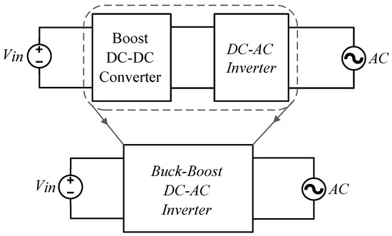
Figure 1.
An illustration of single-stage and two-stage inverter configurations.
As a result, common-ground inverter topologies have been widely studied as an effective solution for reducing leakage current. This is accomplished by directly linking the grid’s neutral and the negative terminals of the PV panels, thereby maintaining constant common-mode voltage. Various single-stage inverters with buck–boost and common-ground functionality have been developed. A common-ground-type inverter with buck–boost functionality was introduced in [13], which offers zero leakage current and wide input voltage range but at the cost of higher complexity and increased switching losses due to multiple switches operating at high frequency in each half-cycle. Similarly, switched-capacitor-based topologies [14,15] achieves high voltage gain and common-mode voltage suppression but requires additional components and complex modulation, which increases the complexity of the design.
To overcome these limitations, a novel common-ground buck–boost inverter (CG-BBI) is proposed, as illustrated in Figure 2. The proposed CG-BBI achieves both buck and boost operation over a wide input-voltage range in a single-stage configuration, without requiring additional DC–DC converters or isolation transformers. It features a reduced component count and establishes a direct common-ground connection between the input and output, which effectively eliminates leakage current and enhances compatibility with PV applications. Furthermore, only two of the switches operate at high switching frequency during each half-cycle, which significantly reduces switching losses and improves overall conversion efficiency.
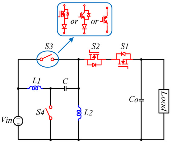
Figure 2.
Proposed structure of single-stage CG-BBI.
2. Modulation Strategy and Operating Modes of CG-BBI Topology
The proposed CG-BBI modulation strategy and the corresponding gate signal generation control block diagram are presented in Figure 3 and Figure 4, respectively. For the interval where the output voltage is positive , as shown in Figure 3, the switch is always ON, and is always OFF while the switches and are switching complementarily at high frequency. For the output voltage to be negative , as shown in Figure 3, the switch remains ON, and stays OFF while the switches and are switching complementarily at high frequency. CG-BBI has four modes of operation throughout a switching cycle. Modes 1 and 2 correspond to the positive half , whereas modes 3 and 4 correspond to the negative half .
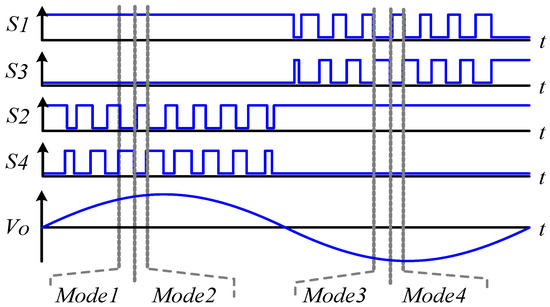
Figure 3.
PWM control scheme for the proposed single-stage CG-BBI.
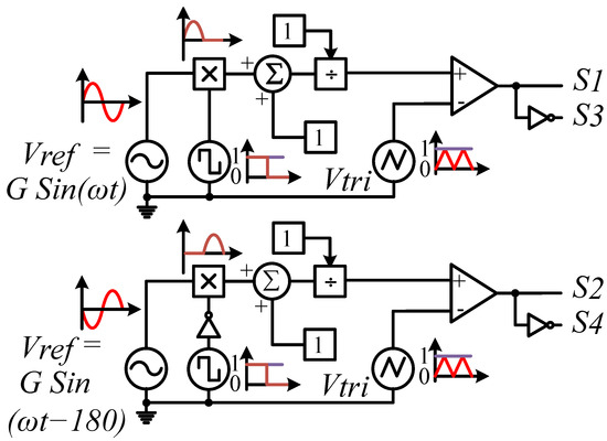
Figure 4.
The proposed structure block diagram for gate signal generation.
To generate a control signal , a reference signal = is multiplied with a rectangular signal of line frequency, having a duty cycle of 0.5 and an amplitude of 1. The resulting half-sinusoidal signal is then added to a constant value of 1. The reciprocal of the resulting DC-biased sinusoidal signal is compared to a 50 kHz triangular carrier (). Similarly, to obtain the gating signal of , the reference signal = is multiplied with the inverted rectangular signal of the line frequency, having a duty cycle of 0.5 and an amplitude of 1. The resulting half-sinusoid is then added to a constant of magnitude 1. Then the reciprocal of this DC-biased half-sinusoid is compared to the triangular carrier () with a 50 kHz switching frequency.
Mode 1: In this operating mode, switches and are turned ON, as illustrated in Figure 5a. Although is ON, no current flows through it due to the reverse-biased body diode of switch . During this interval, diode conducts, allowing inductor to be energized by capacitor C, while the input source simultaneously stores energy in inductor . The voltages appearing across inductors and in this mode are given by
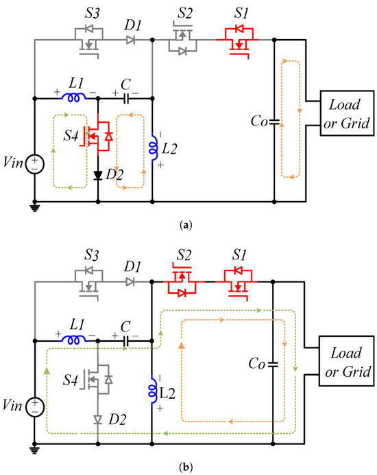
Figure 5.
Modes of operation of CG-BBI for (a) Mode 1 (b) Mode 2.
Mode 2: In this operating mode, and are ON as shown in Figure 5b. The capacitor C is charged, and the inductor is de-energized through the output. The voltages appear on both the inductors and are
The duration of mode 1 is , while the duration of mode 2 is . From the volt–sec balance condition of and , the voltage gain for is
where is the duty ratio of and can alternatively be represented as a function of the voltage gain as
Mode 3: In this operating mode, and are ON, as shown in Figure 6a. Although is ON, no current flows through it due to the reverse-biased body diode of switch . During this interval, diode conducts, and inductor is energized by through switch and diode . The voltages on both the inductors and are
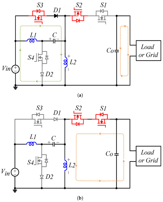
Figure 6.
Modes of operation of CG-BBI for : (a) mode 3, (b) mode 4.
Mode 4: In this operating mode, and are ON, as shown in Figure 6b. The inductor is de-energized through the output in this mode. The voltages appearing on both the inductors and are
The duration of mode 3 is , while the duration of mode 4 is . From the volt–sec balance condition of and , the voltage gain for is
where is the duty ratio of and can alternatively be represented in terms of the voltage gain as
The voltage gain from Equations (7) and (14) is plotted in Figure 7. As observed, the optimal voltage gain approaches infinity when the duty ratio approaches one. Also, a gain in unity is achieved for a duty ratio of 50%. As can be seen in Figure 7, the gain curve is almost linear for duty ratios less than 0.5, corresponding to operation in buck mode. For duty ratios exceeding 50%, the converter operates in boost mode, where the voltage gain exhibits nonlinear behavior with respect to the duty ratio.
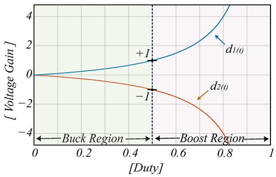
Figure 7.
Voltage gain verses duty ratio curves of the proposed CG-BI.
3. Common-Mode Voltage Analysis
In transformerless PV inverters connected to the grid, leakage current can flow between the PV panels and the grid ground through parasitic capacitances. These capacitances form an unintended path for high-frequency common-mode current, which is primarily driven by variations in the common-mode voltage generated during inverter switching. The resulting leakage current can degrade electromagnetic compatibility (EMC) performance, trigger ground fault protection mechanisms, pose safety risks, and reduce overall system reliability. Therefore, minimizing common-mode voltage variations and effectively mitigating leakage current are critical for meeting safety standards and ensuring stable and reliable inverter operation.
Figure 8a shows the proposed inverter grid-connected configuration, while Figure 8b presents a generalized block diagram of a grid-connected inverter. In Figure 8, P and N represent the positive and negative connections of the PV panel, while and represent the parasitic capacitors. The filter inductors are represented by and . The leakage current depends on the common-mode voltages () and differential-mode voltage (). In Figure 8 the common-mode voltage () and differential-mode voltage () can be found as [16]
where and are output voltages of the inverter, referenced to the negative terminal of the input.
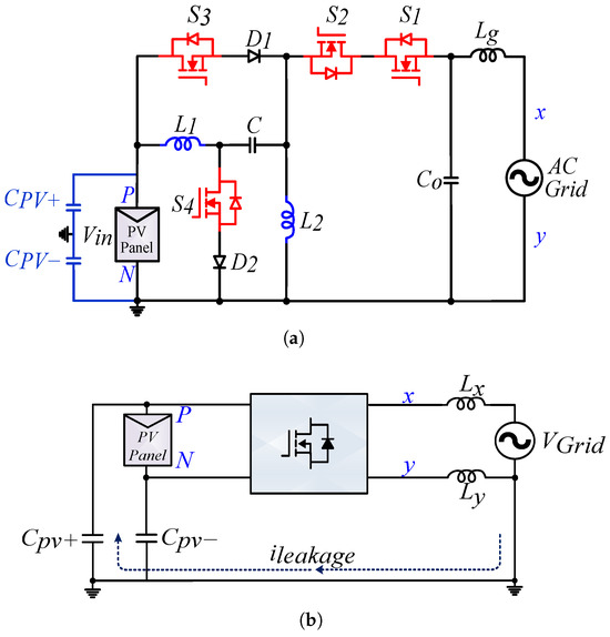
Figure 8.
(a) Proposed CG-BBI topology in grid-connected mode. (b) Block diagram of a typical grid-connected inverter.
The inverters that are connected to a grid are generally categorized as either symmetrical or asymmetrical inductor-based structures. In symmetrical configuration [17,18,19], the inverter input is not directly connected to its output, and two symmetrical output inductors are required to limit the leakage current, which is dependent on given in (15). Unlike symmetrical configurations, the asymmetrical inductor-based inverters need a single output filter inductor, and its output is directly connected to the input [20,21,22]. The leakage current depends on the total common-mode voltages () given as [23]
In the CG-BBI topology shown in Figure 8a, because of the asymmetrical inductor-based inverter configuration, , and therefore the above mentioned equation becomes
Due to the common-ground nature, both ends y and N are shorted. Hence becomes zero, ensuring the absence of any higher switching-frequency common-mode voltage in the proposed inverter.
4. Design Parameters of the Proposed Inverter
4.1. Switch Voltage Stresses
The voltage stress on each switch, relative to maximum output voltage and as a function of voltage gain , are obtained as follows
4.2. Switch Current Stresses
The current stresses on the switches, relative to maximum output current and as a function of voltage gain , are obtained as follows
4.3. Inductor Design
The value of inductors and can be found as a function of voltage gain as
In the above-mentioned equations, , where is equal to . , and is equal to . The value of x is usually selected from 10 to 30. Putting these values in the above equations, the value of inductors can be calculated as
From the above equations, the inductance of the inductors decreases as the voltage gain increases. Therefore, the minimal voltage gain is used to determine it.
4.4. Capacitor Design
Capacitors are designed to suppress the ripples in the output voltage, resulting in smooth output waveform. The capacitance of C and can be derived in term of voltage gain by
where is the ripple of the output voltage and is usually chosen as 5–10% of the output voltage . According to the above equations, the needed capacitance changes as the voltage gain changes. In reality, changing the capacitors in response to variations in voltage gain is not possible. Therefore, a worst-case scenario is selected while designing the capacitors.
4.5. Input Capacitor
The proposed CG-BBI also requires the input DC-link capacitor , like traditional buck–boost inverters. The main objective of the input filter capacitor is to reduce the ripples on the input voltage and provide a stable DC input to the inverter. This capacitor also functions as an energy buffer, ensuring maximum power point tracking (MPPT) operation of a PV system [24]. The required capacitance can be calculated as
where denotes the PV panel power, f is the line frequency, and represents the input voltage ripple, which are typically selected as 5–10% of the input voltage .
5. Simulation Results and Loss Analysis of the CG-BBI
A simulation model for the proposed CG-BBI was built in PSIM to validate its operating principle. The passive circuit parameters of the CG-BBI were selected as H, F and F. The simulation results for both boost and buck operation of CG-BBI are presented in Figure 9 and Figure 10, respectively. For the boost operating mode of the proposed inverter, the input voltage of 100 V was chosen, whereas it was 200 V for buck operation. The output voltage was kept at a constant amplitude with an RMS value of approximately 110 . The simulation was performed at an output power of 500 W, with operating conditions set to a switching frequency of 50 kHz and a line frequency of 60 Hz.
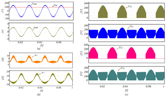
Figure 9.
Boost operating mode of CG-BBI. (a) Input and output voltages along with output current, (b) inductor current, (c) voltage stress on switches.
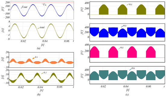
Figure 10.
Buck operating mode of CG-BBI. (a) Input and output voltages along with output current, (b) inductor current, (c) voltage stress on switches.
Figure 9a illustrates the input voltage , output voltage , and output current for the boost operation. It can be observed that, for an input voltage of 100 V, the output reaches a peak of V. The total harmonic distortion (THD) measured in boost mode for a load of 500 W is about and is acceptable according to the IEEE standard 519 . Figure 9b shows the current on both the inductors, and the ripples on both the inductors are less than of the peak inductor current. The switches voltage stresses are represented in Figure 9c. The switches experience voltage stresses, determined by the combined value of the input voltage and peak of the output voltage. Switches are subjected to almost double the input voltage.
Figure 10a illustrates the CG-BBI functionality in buck operating mode, that is, when the desired output voltage is lower than the input voltage. In this case the peak voltage of V is achieved from a 200 V input. The THD measured in buck mode for a load of 500 W is about and is in the acceptable range of less than according to IEEE standard 519 [25]. Figure 10b shows the current through both the inductors. The ripples on the inductors are less than of the peak inductor current. The CG-BBI input and output voltages determine the voltage stress experienced by each switch. The value of the voltage stress on each switch in buck operating mode is greater than that in boost operating mode, as illustrated in Figure 10c.
The main losses in inverters can be broadly categorized into active and passive component losses. Losses associated with active components primarily include the switching and conduction losses of the power switches. In contrast, passive component losses arise from the switching and conduction losses of diodes, the core and winding losses of inductors, and the equivalent series resistance (ESR) of capacitors.
The switching losses are calculated using the data sheet switching energy parameters ( and ) of the UF3CO6504T3S MOSFETs employed in the prototype. These energy values are directly extracted from the data sheet curves of “switching energy’’ versus “junction temperature,” provided for , , and a junction temperature of 100 °C. Based on these parameters, the total switching loss of the proposed converter is evaluated using
The conduction loss of the capacitor is given by
where is the equivalent series resistance, and is the RMS current flowing through the capacitor, expressed as
where T denotes the time period of the line frequency. The core and winding losses of inductors are calculated using the relationships provided in [26]. Core loss may also be approximated from the manufacturer’s core loss chart. A commonly used expression for estimating core loss is
where is a proportionality constant dependent on the operating frequency, is the core cross-sectional area, is the mean magnetic path length, is the peak AC flux density, and is a material-dependent constant obtained from the data sheet Winding losses arise from the DC resistance of the coil as well as skin and proximity effects. The DC winding loss is calculated using
where is the RMS winding current, and is the DC resistance of the inductor windings.
A detailed loss breakdown of the proposed inverter in both buck and boost operating modes at an output power of 500 W and a switching frequency of 50 kHz is provided in Table 1. The same loss analysis methodology is applied to calculate the efficiency across different output power levels for both modes. As shown in Figure 11, the proposed inverter achieves a peak efficiency of 96.46% in buck mode and 96.81% in boost mode at a switching frequency of 50 kHz and an output power of 400 W.

Table 1.
Loss breakdown in buck and boost modes of the proposed inverter at 500 W.
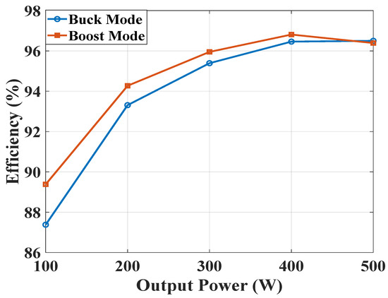
Figure 11.
Efficiency of the proposed inverter for different output powers in both buck and boost modes.
6. Experimental Results of CG-BBI
To validate the theoretical analysis and functionality of the CG-BBI, a 500-W MOSFET-based prototype was fabricated and tested in standalone mode at a switching frequency of 50 kHz. The prototype hardware is shown in Figure 12 and was tested for both buck and boost operating modes. The output voltage was kept constant for both the operating modes, having a peak amplitude of 155.5 V. A summary of the key electrical specifications of the proposed topology are presented in Table 2. The gate driving signals, required for the operation of the inverter, were generated using a TMS320F28379D digital signal processor (DSP).
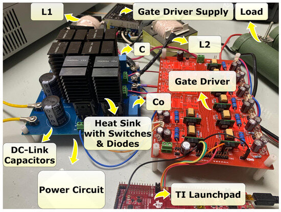
Figure 12.
Prototype of the proposed CG-BBI.
Table 2.
Electrical specifications of components.
The experimental results for CG-BBI in boost operating mode at an input voltage of 100 V are shown in Figure 13. Figure 13a shows the output voltage, input voltage, and output current. Figure 13b shows the and inductor current in boost operating mode. The voltage stresses experienced by the switches are shown in Figure 13c,d. and in the proposed CG-BBI are the voltage stresses on the unidirectional switches, that is, voltage across the MOSFETs’ drain terminal and the cathode of their respective diode connected in series. If reverse-blocking IGBTs are selected, then and in the proposed CG-BBI are the voltage stresses across the reverse-blocking IGBTs.
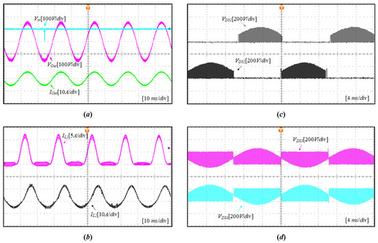
Figure 13.
Experimental evaluation of the CG-BBI operating in boost mode: (a) input and output voltages with the output current; (b) current of inductors , ; (c) voltage stress on switches , ; (d) voltage stress on switches , .
Similarly, Figure 14 shows the experimental validation in buck operating mode, having an input voltage of 200 V. Figure 14a shows the output voltage, input voltage, and output current. Figure 14b shows the current for inductors and in buck operating mode. The voltage stress across the switches in buck operating mode is shown in Figure 14c,d, where and represent the voltage across the unidirectional switches, i.e., MOSFET with series reverse-blocking diode in this case.
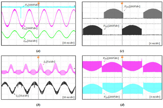
Figure 14.
Experimental evaluation of the CG-BBI operating in buck mode: (a) input and output voltages with the output current; (b) current for inductors , ; (c) voltage stress on switches , ; (d) voltage stress on switches , .
7. Comparative Study
Table 3 presents a comprehensive comparison of CG-BBI with several existing power conversion topologies. CG-BBI achieves a sinusoidal output voltage with an acceptable number of active and passive components. In particular, only four active switches are required for both the buck and boost modes of operation. The comparison considers key performance criteria that include the number of components, the number of input sources, the ability to eliminate leakage current, and support for a wide input voltage range. Among the examined topologies, CG-BBI consistently demonstrates fewer active components, making it a promising candidate for compact and efficient design.
Table 3.
Comparison of the proposed CG-BBI with other buck–boost inverters.
The inverter topology reported in [27] maintains a constant common-mode voltage throughout a switching cycle, thereby mitigating the leakage current. However, its input voltage must be greater than the output, and needs a front-stage boost converter. Also, it has more high-frequency-switching active components and increased switching losses, and the diodes in the current path further increase the total loss. Unlike the other structures, the inverters in [28,29] have the same switch count as CG-BBI and eliminate leakage current. But, these inverters are also limited to buck operating mode and need an external boost stage, which increases the number of components count and complexity. Also, its reliance on a front-end boost converter compromises overall system efficiency, as the total efficiency is the product of both DC–DC and DC–AC conversion efficiencies.
Similarly, the inverter in [30] uses fewer active switches and requires a high step-up front-stage converter, leading to a significant increase in passive components and structural complexity. A quasi-single-stage common-ground inverter is presented in [31], utilizing four active switches, and effectively eliminates the leakage current while enabling voltage boosting. However, all the switches operate at higher switching frequencies during the negative cycle, resulting in increased switching losses. Moreover, larger numbers of diodes and switches are present in the conduction path during each switching cycle, further contributing to conduction losses. The inverter topology presented in [32] exhibits negligible leakage current and is capable of achieving a wide voltage range and high gain; however, it suffers from higher stresses on the active components.
Overall, the comparative study demonstrates that the proposed CG-BBI topology achieves a superior balance between topology complexity, leakage current mitigation, and width of voltage range. Unlike other solutions that rely on additional front-end converters or suffer from higher switching and conduction losses, CG-BBI provides an inherently compact and efficient architecture. Its versatility and simplicity make it an excellent choice for single-phase transformerless inverters in photovoltaic applications, where maximizing efficiency and reliability while reducing complexity are critical design objectives.
8. Conclusions
A novel single-stage, four-switch common-ground buck–boost inverter (CG-BBI) topology was proposed in this work. The topology provides both buck and boost operation without requiring an additional DC–DC converter or isolation transformer, while the common-ground configuration effectively suppresses the leakage current. The employed modulation strategy allows only two devices to operate at high switching frequency during each half cycle, resulting in significantly reduced overall switching losses and improved conversion efficiency. PSIM-based simulations and experimental results obtained from a laboratory-scale prototype demonstrate stable output voltage regulation at 110 Vrms in both buck and boost operating modes. Operation near the unity power factor confirms the suitability of the proposed inverter for grid-connected photovoltaic (PV) applications. By combining single-stage buck–boost functionality, leakage current suppression, efficient power conversion, and robust operation, the proposed CG-BBI presents a practical and compact solution for single-phase transformerless inverters, highlighting its potential for efficient and reliable PV system integration.
Author Contributions
Conceptualization, A.U. and Y.-O.C.; Methodology, A.U., Y.-H.P. and Y.-O.C.; Software, A.U.; Validation, Y.-O.C.; Formal analysis, A.U.; Investigation, Y.-H.P.; Resources, A.U. and Y.-H.P.; Data curation, A.U. and Y.-H.P.; Writing—original draft, A.U.; Writing—review and editing, Y.-O.C.; Visualization, Y.-H.P.; Supervision, Y.-O.C.; Project administration, Y.-O.C.; Funding acquisition, Y.-O.C. All authors have read and agreed to the published version of the manuscript.
Funding
This work was supported by a Gwangju Jeonnam Local Energy Cluster Human Resources Development of the Korea Institute of Energy Technology Evaluation and Planning (KETEP) grant funded by the Korea government Ministry of Trade, Industry and Energy (No. RS-2021-KP002519).
Data Availability Statement
The original contributions presented in this study are included in the article. Further inquiries can be directed to the corresponding author.
Conflicts of Interest
The authors declare no conflicts of interest.
Abbreviations
| AC | Alternating Current |
| CSI | Current-Source Inverter |
| CG-BBI | Common Ground Buck–Boost Inverter |
| CMV | Common-Mode Voltage |
| DC | Direct Current |
| DSP | Digital Signal Processor |
| EMC | Electromagnetic Compatibility |
| ESR | Equivalent Series Resistance |
| HF | High Frequency |
| IGBT | Insulated Gate Bipolar Transistor |
| IEEE | Institute of Electrical and Electronics Engineers |
| LF | Low Frequency |
| MOSFET | Metal–Oxide Semiconductor Field-Effect Transistor |
| MPPT | Maximum Power Point Tracking |
| PV | Photovoltaic |
| PWM | Pulse Width Modulation |
| PSIM | Power Simulation Software |
| RMS | Root Mean Square |
| SiC | Silicon Carbide |
| THD | Total Harmonic Distortion |
| VSI | Voltage Source Inverter |
References
- Azmi, S.A.; Ahmed, K.H.; Finney, S.J.; Williams, B.W. Comparative analysis between voltage and current source inverters in grid-connected application. In Proceedings of the IET Conference on Renewable Power Generation (RPG 2011), Edinburgh, UK, 6–8 September 2011; IET Conference Publications: Stevenage, UK, 2011. [Google Scholar] [CrossRef]
- Lee, S.; Chen, F.; Jahns, T.M.; Sarlioglu, B. Review on Switching Device Fault, Protection, and Fault-Tolerant Topologies of Current Source Inverter. In Proceedings of the 2021 IEEE 13th International Symposium on Diagnostics for Electrical Machines, Power Electronics and Drives, SDEMPED 2021, Dallas, TX, USA, 22–25 August 2021. [Google Scholar] [CrossRef]
- Kabalcı, E. Review on novel single-phase grid-connected solar inverters: Circuits and control methods. Sol. Energy 2020, 198, 247–274. [Google Scholar] [CrossRef]
- Kjaer, S.B.; Pedersen, J.K.; Blaabjerg, F. A review of single-phase grid-connected inverters for photovoltaic modules. IEEE Trans. Ind. Appl. 2005, 41, 1292–1306. [Google Scholar] [CrossRef]
- Pan, X.; Gu, Y.; Wang, P.; Rathore, A.K. Novel hybrid modulation based isolated high-frequency bidirectional inverter for microgrid application. In Proceedings of the IECON 2016—42nd Annual Conference of the IEEE Industrial Electronics Society, Florence, Italy, 23–26 October 2016; pp. 3517–3522. [Google Scholar] [CrossRef]
- Lai, R.S.; Ngo, K.D.T. A PWM method for reduction of switching loss in a full-bridge inverter. In Proceedings of the 1994 IEEE Applied Power Electronics Conference and Exposition—ASPEC’94, Orlando, FL, USA, 13–17 February 1994; Volume 1, pp. 122–127. [Google Scholar] [CrossRef]
- Hasan, K.; Yousuf, S.B.; Tushar, M.S.H.K.; Das, B.K.; Das, P.; Islam, M.S. Effects of different environmental and operational factors on the PV performance: A comprehensive review. Energy Sci. Eng. 2022, 10, 656–675. [Google Scholar] [CrossRef]
- Chang, C.-H.; Cheng, C.-A.; Chi, C.-C.; Chen, Y.-Y. Design and implementation of a single-phase buck–boost inverter. In Proceedings of the 2017 IEEE 3rd International Future Energy Electronics Conference and ECCE Asia (IFEEC 2017—ECCE Asia), Kaohsiung, Taiwan, 3–7 June 2017; pp. 1419–1424. [Google Scholar] [CrossRef]
- Wu, T.F.; Kuo, C.L.; Sun, K.H.; Chen, Y.K.; Chang, Y.R.; Lee, Y.d. Integration and operation of a single-phase bidirectional inverter with two buck/boost MPPTs for DC-distribution applications. IEEE Trans. Power Electron. 2013, 28, 5098–5106. [Google Scholar] [CrossRef]
- Gonzalez, R.; Lopez, J.; Sanchis, P.; Marroyo, L. Transformerless inverter for single-phase photovoltaic systems. IEEE Trans. Power Electron. 2007, 22, 693–697. [Google Scholar] [CrossRef]
- Ji, B.; Wang, J.; Zhao, J. High-efficiency single-phase transformerless PV H6 inverter with hybrid modulation method. IEEE Trans. Ind. Electron. 2013, 60, 2104–2115. [Google Scholar] [CrossRef]
- Wang, J.; Luo, F.; Ji, Z.; Sun, Y.; Ji, B.; Gu, W.; Zhao, J. An Improved Hybrid Modulation Method for the Single-Phase H6 Inverter with Reactive Power Compensation. IEEE Trans. Power Electron. 2018, 33, 7674–7683. [Google Scholar] [CrossRef]
- Vosoughi, N.; Hosseini, S.H.; Sabahi, M. A New single-phase transformerless grid-connected inverter with boosting ability and common ground feature. IEEE Trans. Ind. Electron. 2020, 67, 9313–9325. [Google Scholar] [CrossRef]
- Estévez-Bén, A.A.; Alvarez-Diazcomas, A.; Macias-Bobadilla, G.; Rodríguez-Reséndiz, J. Leakage current reduction in single-phase grid-connected inverters—A review. Appl. Sci. 2020, 10, 2384. [Google Scholar] [CrossRef]
- Salem, A.; Sedraoui, K. Highly efficient transformerless inverter with flying-capacitor buck–boost for single-phase grid-connected pv systems. Appl. Sci. 2021, 11, 10841. [Google Scholar] [CrossRef]
- Li, W.; Gu, Y.; Luo, H.; Cui, W.; He, X.; Xia, C. Topology review and derivation methodology of single-phase transformerless photovoltaic inverters for leakage current suppression. IEEE Trans. Ind. Electron. 2015, 62, 4537–4551. [Google Scholar] [CrossRef]
- Zhang, L.; Sun, K.; Xing, Y.; Xing, M. H6 transformerless full-bridge PV grid-tied inverters. IEEE Trans. Power Electron. 2014, 29, 1229–1238. [Google Scholar] [CrossRef]
- Desai, A.A.; Mikkili, S.; Senjyu, T. Novel H6 transformerless inverter for grid-connected photovoltaic system to reduce the conduction loss and enhance efficiency. Energies 2022, 15, 3789. [Google Scholar] [CrossRef]
- Wang, J.; Gao, S.; Sun, Y.; Ji, Z.; Cheng, L.; Li, L.; Gu, W.; Zhao, J. Single phase bidirectional H6 rectifier/inverter. IEEE Trans. Power Electron. 2019, 34, 10711–10722. [Google Scholar] [CrossRef]
- Akbar, F.; Cha, H.; Kim, H.G. Novel virtual-ground single-stage single-inductor transformerless buck–boost inverter. IEEE Trans. Ind. Electron. 2021, 68, 6477–6487. [Google Scholar] [CrossRef]
- Gu, Y.; Li, W.; Zhao, Y.; Yang, B.; Li, C.; He, X. Transformerless inverter with virtual DC bus concept for cost-effective grid-connected PV power systems. IEEE Trans. Power Electron. 2013, 28, 793–805. [Google Scholar] [CrossRef]
- Akbar, F.; Elkhateb, A.; Ahmed, H.F.; Khan, A.A.; Cha, H.; Park, J.W. Single-phase virtual-ground transformerless buck–boost inverters. IEEE Trans. Power Electron. 2023, 38, 10401–10413. [Google Scholar] [CrossRef]
- Vosoughi, N.; Hosseini, S.H.; Sabahi, M. A New Transformer-Less Five-Level Grid-Tied Inverter for Photovoltaic Applications. IEEE Trans. Energy Convers. 2020, 35, 106–118. [Google Scholar] [CrossRef]
- El Aamri, F.; Maker, H.; Sera, D.; Spataru, S.V.; Guerrero, J.M.; Mouhsen, A. A direct maximum power point tracking method for single-phase grid-connected PV inverters. IEEE Trans. Power Electron. 2018, 33, 8961–8971. [Google Scholar] [CrossRef]
- IEEE 519-2022; IEEE Standard for Harmonic Control in Electric Power Systems (Revision of IEEE Std 519-2014). IEEE: New York, NY, USA, 2022. [CrossRef]
- Erickson, R.W.; Maksimovic, D. Fundamentals of Power Electronics, 3rd ed.; Springer: Norwell, MA, USA, 2001; Chapter 12. [Google Scholar]
- Xiao, H.F.; Lan, K.; Zhang, L. A quasi-unipolar SPWM full-bridge transformerless PV grid-connected inverter with constant common-mode voltage. IEEE Trans. Power Electron. 2015, 30, 3122–3132. [Google Scholar] [CrossRef]
- Ardashir, J.F.; Sabahi, M.; Hosseini, S.H.; Blaabjerg, F.; Babaei, E.; Gharehpetian, G.B. A Single-Phase Transformerless Inverter with Charge Pump Circuit Concept for Grid-Tied PV Applications. IEEE Trans. Ind. Electron. 2017, 64, 5403–5415. [Google Scholar] [CrossRef]
- Damodaran, R.V.; Shareef, H.; Errouissi, R.; Eslami, M. A Common Ground Four Quadrant Buck Converter for DC-AC Conversion. IEEE Access 2022, 10, 44855–44868. [Google Scholar] [CrossRef]
- Sarikhani, A.; Ghaderi, M.H.; Hamzeh, M. A Common-Ground Quazi-Z-Source Single-Phase Inverter Suitable for Photovoltaic Applications. IEEE Trans. Energy Convers. 2021, 36, 594–601. [Google Scholar] [CrossRef]
- Peng, F.; Zhou, G.; Xu, N.; Gao, S. Zero Leakage Current Single-Phase Quasi-Single-Stage Transformerless PV Inverter with Unipolar SPWM. IEEE Trans. Power Electron. 2022, 37, 13755–13766. [Google Scholar] [CrossRef]
- Oppong, F.N.; Ahmed, H.F.; Khan, A.A.; Quaicoe, J.E. High-Gain Single-Stage Single-Phase Common-Ground Buck–Boost Inverter. IEEE Trans. Power Electron. 2025, 40, 1074–1084. [Google Scholar] [CrossRef]


Disclaimer/Publisher’s Note: The statements, opinions and data contained in all publications are solely those of the individual author(s) and contributor(s) and not of MDPI and/or the editor(s). MDPI and/or the editor(s) disclaim responsibility for any injury to people or property resulting from any ideas, methods, instructions or products referred to in the content. |
© 2025 by the authors. Licensee MDPI, Basel, Switzerland. This article is an open access article distributed under the terms and conditions of the Creative Commons Attribution (CC BY) license.