Abstract
Power semiconductor devices are fundamental components in modern electronic power conversion. In applications demanding high power density and efficiency, the choice between silicon (Si) IGBTs and Silicon Carbide (SiC) MOSFETs is critical. SiC MOSFETs, owing to their high critical electric field, superior thermal conductivity, wide band gap, and low power loss, realize significant performance improvements and compact design. This work presents a comprehensive, simulation-driven comparative investigation under identical setups, evaluating both technologies across various parameters. The effects of temperature variations on gate-source threshold voltage drift, current slew rate, device stress, and energy dissipation during switching transitions are evaluated. Furthermore, the characteristic switching behavior when the DC-bus voltage, gate resistance, and load current are varied is investigated. This study addresses a current scarcity of systematic investigation by presenting a comprehensive comparative evaluation of switching losses and efficiency across varied operating conditions, providing validated conclusions for the design of advanced WBG converters. The results demonstrate that SiC exhibits lower losses and faster switching speeds than Si IGBTs, with minimal temperature-dependent loss variations, unlike Si devices, whose losses rise significantly with temperature. Si shows distinct tail currents during turn-off, absent in SiC devices. A conclusive comparative evaluation of switching energy losses under varied operating conditions demonstrates that SiC devices can effectively retrofit Si counterparts for fast, low-loss, high-efficiency applications.
1. Introduction
In comparison with the material properties of Silicon (Si) IGBT, Silicon Carbide (SiC) MOSFET proves to be advantageous in having a Wide Band Gap (WBG) energy, a critical electrical field, and thermal conductivity. A higher electrical field enables the device to withstand higher voltages, reduce resistance, and achieve lower conduction loss [1,2,3]. The high thermal properties allow for a compact size due to their small cooling requirements and significantly improve the power density. Additionally, the SiC MOSFETs have various advantages, such as higher blocking voltage capability, higher switching frequency, higher voltage, and the ability to operate at relatively higher junction temperatures [4,5]. Moreover, SiC exhibits superior switching characteristics compared to its counterpart Si devices, which has an impact on the switching loss as well as the passive magnetic components utilized. Additionally, the technical maturity of the commercially available SiC-WBG devices acts as a catalyst for rapid and transformative advances in power electronics devices. This significantly affects power utility applications, as they are preferred, considering their high efficiency and frequency capability [6].
This work aims to investigate the differences in switching characteristics between Si and SiC MOSFET devices, including the various losses and the effects resulting from variation in parameters, such as parasitic effects and temperature fluctuations in both devices. Traditionally, Si-based power devices have dominated the power converter industry. However, with the increased penetration of renewable energies, efficient storage systems, and high-voltage DC systems, their theoretical limits have been saturated. The increased switching losses act as a hindrance when the device is operated at high frequencies and voltages [7]. Especially during the turn-off, since the majority carrier injected in the drift region during the forward conduction results in a tail current. This results in a very slow turn-off and high turn-off losses due to the absence of an intrinsic body diode in Si devices; a high reverse recovery current is needed, which leads to a high overshoot through the device during the turn-on, leading to a high loss during the turn-on process. With the limitations above, high-end power conversion devices are being sought. WBG devices become a better alternative and are thus given detailed attention. The premium in SiC enables higher temperature operation with a more dense system design [8]. Additionally, the SiC MOSFET on-state resistance has remarkably reduced, thus achieving an incredibly high current and voltage performance [9,10]. It is observed that the switching patterns of the SiC MOSFET are predictable, as it performs zero-voltage transitions. Again, the SiC devices do not have the turn-off tail currents and forward voltage drop during transitions. In addition, the device endures less stress and small ripple currents; thus, it exhibits better Electromagnetic Interference (EMI) performance and higher efficiency. Combining the excellent switching performance of SBD and the elevated switching speed of SiC devices results in the device working at higher frequencies in both soft and hard-switching converter technology, resulting in reduced active volume of passive elements, with ultimate compact converters [11,12,13,14,15].
Enhanced switching speed offers an advantage in reducing switching loss, minimizing the passive components, and decreasing the size of the heat sink, thereby achieving higher efficiency and frequency [16]. When the Si material properties are compared with their counterpart SiC, the latter exhibits numerous advantages in their high thermal conductivity value (i.e., 3× than that of Si), larger wide band gap values (i.e., 3× than that of Si), critical electrical field (i.e., 10× that of Si), low intrinsic carrier concentration, carrier mobility, higher breakdown electrical fields, higher thermal conductivity, larger saturation electric drift velocity (i.e., 2× that of Si), and higher radiation resistance, among others [4,17,18]. The comparison of these physical properties is shown in Figure 1 for Si and SiC.
However, despite the above-listed strong characteristics of the SiC MOSFET, full adoption remains a challenge. This is contributed to by the global chain manufacturing and module packaging still being relatively in the evolutionary stages. In comparison, Si technology is highly cost-optimized and highly standardized, mature technology. The theoretical benefits of SiC devices cannot be fully realized, as advanced packaging is still complex and costly, and partial discharge and thermal stress hinder total transition [19,20]. For the WBG devices, the fast switching transitions, despite being a merit, introduce higher and , which consequently exacerbate the common mode emissions in the conductive EMI frequency range, calling for expensive filtering requirements, compared to slower switching transitions in Si devices, which do not require expensive filtering [21,22]. In addition, the SiC device constitutes a smaller chip area in comparison with Si IGBTs with the same voltage-current ratings. This leads to high short-circuit current density as well as smaller heat capacity. Ultimately, the short-circuit withstand capability of the WBG devices is less than that of Si devices. This implies that the SiC devices’ gate failure in a short circuit or thermal runaway can be reached in a few microseconds [23]. The SiC, unlike Si devices, requires tighter gate voltage and current margins (−5 V/+18 V), and has a lower threshold voltage, drift, and is highly susceptible to parasitic turn-on due to high [24,25]. Amongst other limitations, these factors render SiC less economically viable in comparison with Si in applications where premium performance is not required. Finally, the practical utilization of the SiC devices comes with the constraint of significantly higher gate drive complexity for EMI suppression [26] and rigorous layout optimization to mitigate inductance-induced voltage overshoots. These critical issues in SiC are less prevalent in Si since it is more robust [27].

Figure 1.
Comparison of physical material properties of Si and SiC MOSFETs [18,28].
Figure 1.
Comparison of physical material properties of Si and SiC MOSFETs [18,28].

Although the SiC device is more expensive than the mature Si technology devices, its high switching frequency makes it compact, thus requiring a small cooling system, which translates to lower total cost. However, due to their narrow Short-Circuit Safe Operation Area (SCSOA), they have shorter withstand times in comparison with the Si device; thus, their practical implementation necessitates a more stringent and fast protection method to mitigate the risk associated with their reduced thermal capacity during the fault period [29].
Despite the performance of the discrete SiC MOSFET being discussed in various publications, such as the authors of [30,31] did a comparison of thermal, , and and transient signals with similar parameters, few have considered the performance when various parameters are varied. This paper investigates the performance of the Wolfspeed C3M0075120D SiC MOSFET with a SiC Schottky Barrier Diode (SBD) module, comparing it with the Rohm RGC80TSX8R Si IGBT and a diode module, with an emphasis on performance and efficiency under variations in various parameters. Further, this paper will present a characterization of both the Si and SiC devices under static and dynamic switching states in different operating conditions. Their various performances under various operational conditions will be given.
The main contribution of this work is the presentation of an in-depth comparative evaluation and analysis of Si and SiC modules with similar related conditions and thermal characteristics. This comparison is based on the identical simulation platform, gate driver standards as close as possible, while being conducted at operating points that simulate industrial converters, which would be used when operating these devices. Therefore, this provides the most sought-after technical background information for selecting the right module over others, depending on specific application requirements. Additionally, the SiC power MOSFET has low on-state resistance , which makes the device integration preferred due to lower losses and manageable thermal performance. With this, a stable temperature operation is observed, making the device operation very rugged while the mounting of the heat sink is applicable with possible low junction-to-case thermal resistance [17].
This paper is organized as follows: In Section 2, a comprehensive description of the inductive load Double Pulse Test (DPT) is provided, along with its commutation process. In Section 3, the dynamic characteristics of the transient signals and losses are presented and discussed. Section 4 presents the efficiency associated with the Si IGBT and SiC MOSFET devices, and finally, a brief discussion and conclusion are given.
2. Modeling Analysis of Si IGBT and SiC MOSFET
2.1. Circuit Modeling and Simulation Methodology
The evaluation of the dynamic behavior of the SiC and Si power devices, taking into consideration the accuracy and speed, involved a robust circuit simulation. The circuit comprises model parameters that can be extracted straightforwardly when the manufacturer’s data sheet is available. The model comprises intrinsic elements, such as the gate resistance, capacitance, and load currents, among others, to emulate the real switching conditions of the devices closely. The simulation setup configuration allows the extraction of the transition energy loss, conduction characteristics, influence of temperature, DC bus voltage, and load current on the devices. As a result of this, the LTspice Simulation Software V24.1.10 was used [32]. This modeling approach has merit in that it ensures a reliable correlation between the device parameters and their impact on the performance of the converter.
This study was critically evaluated using manufacturer-verified high-fidelity Spice models, which provide reliable insights into the switching transient behavior of the switching devices, closely presenting the actual physical Si and SiC devices’ evaluated behavior. Consequently, the simulation results provide a credible foundation for understanding the guiding practical design optimization, with future experimental verification.
2.2. The Double Pulse Test (DPT) Platform
Switching transient contributes the highest portion of losses at elevated frequency. To evaluate the performance of the Si and SiC devices, an inductive load Double Pulse Test (DPT) setup was designed and implemented in LTspice simulation software V24.1.10 to characterize the switching performance and losses during turn-on (turn-off) of the Si and SiC switching devices. In the foregoing studies, instead of using entirely different gate driver typologies, the tests for the two devices use a similar configuration with a few different key components to ensure uniformity. To maintain the level of stray inductance, devices with the same housing structure were chosen.
The circuit of the DPT is shown in Figure 2a. This is utilized in testing the switching behaviors of the switch devices during the turn-on and turn-off transitions [33,34,35]. The DPT comprises the power supply (), the gate drive circuitry, a supply voltage stabilizing capacitor during the test, the load inductor, and the free-wheeling diode. Figure 2b shows the basic ideal waveform for drain–current and drain–source voltage during the transition events.
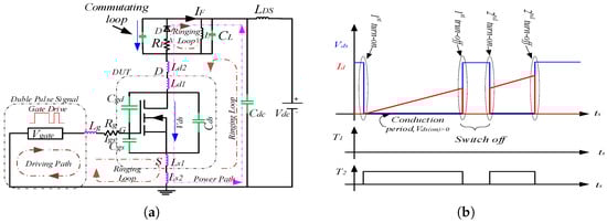
Figure 2.
Equivalent basic load switching model of the double pulse test used to test Si IGBT and SiC MOSFET. (a) Equivalent schematic diagram used for a basic DPT test. (b) Basic waveforms showing the turn-on and turn-off points for and .
Since semiconductor devices used in the tests have different gate drive characteristics, as noted from their respective manufacturers’ data sheets, the gate minimum/maximum drive voltage of SiC (gate–source voltage) and Si (gate–emitter voltage) are −8 V/+19 V and −30 V/+30 V, respectively. A gate driver with a maximum gate voltage source swing of −4 V/+15 V and −5 V/+20 V signals ensured that the switching devices were switching appropriately since the gate threshold voltage, , is 2.5 V and 6.0 V for SiC and Si, respectively. The LTspice simulation was configured to calculate the average switching power dissipation over a period of , which corresponded to a switching frequency of 33.3 kHz. The high gate voltage, higher than the gate threshold voltage of the respective devices, ensured that there is no spurious triggering, which would otherwise lead to noise and parasitic coupling. The negative gate voltage during the device turn-off ensures reliable turn-off, and there is no spurious turn-on. SiC, having a higher gate drive voltage, can significantly minimize the conduction resistance; however, the switching speed does not change since it is determined by the gate resistance rather than the input maximum gate voltage. Both devices are equipped with internal resistors whose work is to prevent unwanted oscillations between the connected parallel chips in the module; unfortunately, these can not be altered or varied from the outside.
The external gate resistor is a good candidate to control the voltage overshoot, the switching speed, and the slew rate () of the device, though this is not practical for all the values of the load current . The selection of the gate resistance comes as a balance between ringing, overshoots, EMI, cross-talk effects, and switching loss. Thus, optimum gate resistance should be chosen for both gate drivers. It is noted that the SiC over-voltages result from the stray inductance of the device commutation loop and the switching speed. In contrast, for the Si, it comprises the peak forward voltage of the free-wheeling diode and the stray inductance on the device. The Si turn-off over-voltage comprises a high peak dynamic forward voltage, whereas SiC does not show dynamic forward voltage. When the stray inductance and overshoot voltage were the same, the SiC showed an ability to clear faster during the turn-off [36].
The main parameters of the Double Pulse Test (DPT) were introduced as follows: The main Device Under Test (DUT) is a commercially available SiC MOSFET from Wolf-speed C3M0075120D [37], in a TO-247-3 package, and a Discrete SiC Schottky Barrier Diode (SBD), also from Wolf-speed C4D20120A (1200V, 20A) in a TO-220-2 package. For comparison, a Rohm RGC80TSX8R Field Stop Trench IGBT in a TO-247N package was chosen [38]. The typical characterizing parameters, such as the input capacitance , output capacitance , and the reverse transfer capacitance, also known as the Miller Capacitance , of the modules used are listed in Table 1. Moreover, other details of the parameters of the Si and SiC devices used are listed. The gate change is indicated as is 54 nC for the SiC and 468 nC for the Si device. The higher value of in Si IGBT has a disadvantage in that it increases the cost of the gate driver, the driver power losses, and the component costs, besides driver complexity [39]. Moreover, eliminating the stored charges during the conduction-to-blocking transitions leads to a high reverse recovery current spike, voltage overshoot, and significant switching loss. Additionally, the internal gate resistance of the SiC and IGBT module is and , respectively. A slightly higher value of acts as a limiter to the switching speed of the device. Manufacturers intentionally use a higher intrinsic gate resistance to dampen the gate oscillations associated with and in SiC devices. Both devices are usually designed with internal gate resistance to ensure that the oscillations between the parallel-connected chips within the model are maintained as low as possible [36].

Table 1.
Comparison of data-sheet parameters for SiC MOSFET (C3M0075120D) and Si IGBT (RGC80TSX8R) at C.
To ensure the simulation results accurately reflect the real environment setup and switching transient, stray inductance was included in the model. The PCB power loop lumped inductance was taken as 10 nH, and the gate loop parasitic inductance was 2 nH. Furthermore, to account for the discrete device package parasitic, the simulation included drain, source, and gate inductance of 5 nH, 2 nH, and 10 nH, respectively. The drain–source parasitic capacitance , gate–source parasitic capacitance , and gate–drain parasitic capacitance used in the simulations were 84.5 pF, 1122.5 pF, and 7.5 pF, respectively.
The SiC-enhanced switching characteristics illustrate a significant switching loss reduction. Despite the Si’s ability to withstand low resistance and slightly higher voltage, the tail current significantly increases losses. In contrast, the SiC can withstand very high voltages, high switching speeds, and low on-state resistance, attributed to the significant WBG. It is remarkable to see that the time required for the convergence conditions is overwhelmingly faster in SiC than in Si devices. The extended time taken by Si devices contributes to the loss of energy. Additionally, the turn-on current through the device includes the diode recovery current, inbuilt or external, which is between the IGBT’s collector, and this contributes to the effects of diode recovery characteristics.
It is noted that a large value of prolongs the turn-on delay and current rise time but does not change the gate signal, as can be seen in Figure 3 and Figure 4. From these two figures, the device has been characterized under different operating conditions with = 800 V and a varied gate resistance . Specifically, the transient have been captured at = , , , , and . Furthermore, as the value of is increased, the amount of energy lost increases. The gate resistance has a strong influence on the turn-on and turn-off energy dissipation. Smaller gate resistance implies a lower switching loss, though, on the other hand, very small gate resistance increases the device loss and current-voltage ridging. The summation of the energy loss indicates that the energy loss is proportional to the value of the gate resistance. Figure 5 points out that when the value of = , the turn-on energy loss is 0.76 mJ and 1.03 mJ, and the turn-off energy loss is 0.45 mJ and 1.32 mJ for SiC and Si, respectively. Increasing the linearly increases the turn-on energy loss to 0.95 mJ and 2.24 mJ, while the turn-off energy increases to 0.70 mJ and 5.02 mJ for SiC and Si, respectively. A clear indication that the turn-off energy, especially in the Si device, is significantly high due to the tail current associated with its turn-off process, when the value of gate resistance is high. The other values of turn-on (turn-off) energy loss in the range of the different resistances are shown in Table 2.
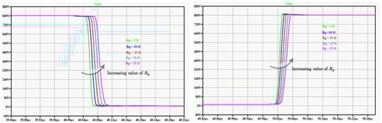
Figure 3.
Analytically switching waveform showing turn-on (left) and turn-off (right) transient voltage (Vds) of a SiC MOSFET, illustrating the effects of different gate resistors ( = 1–5 Ω) under a supply voltage of 800 V (Vdc). (Time (20 ns/div).
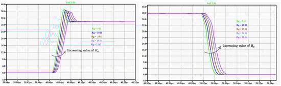
Figure 4.
Analytically switching waveform showing turn-on (left) and turn-off (right) transient current (Ids) of a SiC MOSFET, illustrating the effects of different gate resistors ( = 1–5 Ω) under a supply voltage of 800 V (Vdc). (Time (20 ns/div).
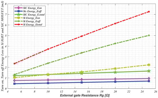
Figure 5.
Comparison of physical properties of Si and SiC MOSFETs: turn-on, turn-off, and total energy loss at different gate resistors (–).
Table 2.
Switching energy losses for SiC MOSFET (C3M0075120D) and Si IGBT (RGC80TSX8R) under different gate resistances.
Table 3 below shows a summary of the effects associated with increasing and decreasing the value of gate resistance and the various influences on different parameters of typical SiC and Si devices during the turn-on (turn-off) switching transitions. As mentioned previously, it can be clearly deduced that when the value of is raised, the gate voltage transitions slow down, consequently increasing the turn-on (turn-off) transition time (, ), ultimately leading to increased switching energy loss (, ). The ultimate result is lowered current and voltage slew rates (, ), implying reduced voltage overshoots, reduced peak and recovery currents, and reduced EMI noise, which provides a safer, smoother switching process, though at the expense of efficiency. Notably, the converse is true for a smaller .
Table 3.
Switching behavior by changes in the gate resistor.
A thorough comparison of Si IGBT modules and SiC MOSFET modules operated under the same conditions is shown in Table 4. The SiC, as shown, achieves faster switching and higher slew rates, leading to lower losses and weaker temperature dependence compared to Si. Nonetheless, increasing the speed of operation raises noise and cross-talk [40].
Table 4.
SiC MOSFET electrical parameters.
2.3. The Switching Behavior of the Si IGBT and SiC MOSFET
Figure 6 and Figure 7 illustrate the quantified turn-on and turn-off switching behavior of the Si and SiC devices. To have a better visibility of this illustration, the two waveforms are placed on the same scale. These devices have been tested with input constants, which are the dc-link voltage source = , the output current, which is modeled as a constant current source , and the gate signal , which flips between −4 V and . In Figure 6, the SiC demonstrates a significantly faster voltage drop during turn-on, with a clean transition and minimal oscillations, in comparison with the Si device dynamic curve, which exhibits a slower voltage decrease and a delayed current rise due to higher gate resistance and minority carrier effects. The said delay contributes to significant switching losses in Si compared to SiC devices. Conversely, Figure 7 shows the turn-off dynamic characteristic, in which the SiC MOSFET shows a great performance against the Si IGBT. This is because the SiC exhibits rapid voltage recovery with minimal ringing, whereas the Si shows a pronounced tail current, which further increases turn-off switching losses. Generally, from the two figures, it is clearly observed that the SiC device showcases superior switching performances with reduced energy loss and enhanced dynamic switching characteristics, making it superior for high-efficiency and high-frequency operations.
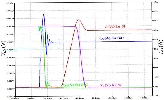
Figure 6.
Switching behavior of Si and SiC MOSFETs during turn-on, with equal voltage (, 10 ns/div).
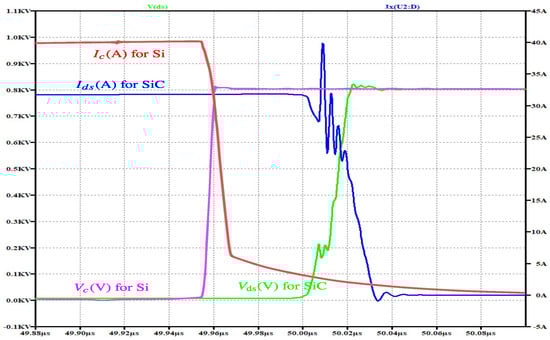
Figure 7.
Dynamic characteristics waveforms of Si and SiC MOSFETs during turn-off (, 10 ns/div).
Figure 8 is an illustration of a double pulse test transient for a Si IGBT. The green curve shows the , and the blue shows the . Similarly, Figure 9 shows the transient of the SiC MOSFET device. The tests are carried out when both are under nominal design conditions, i.e., with the same value of gate resistance. The DPT transient was compared at a supply voltage of 800V. In the case of the SiC device, a small value of gate charge is required to switch on the device, and the low transconductance aids in eliminating the Miller plateau, which is observed in the Si devices. Additionally, the Si during the turn-off transitions has a visible current tail, which increases the current fall time, whereas the SiC device has a fast fall time, hence a lower transitional time. This transitions to a lower turn-off time in Sic in comparison with Si devices.
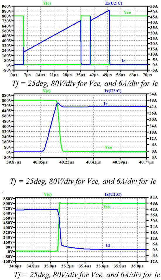
Figure 8.
Full DPT transient for Si IGBT, zoomed view of the Si IGBT turn-on transitions and turn-off transition.
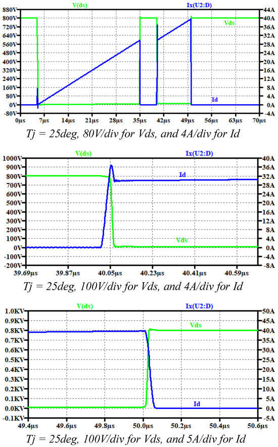
Figure 9.
Full DPT transient for Si MOSFET, zoomed view of the SiC MOSFET turn-on transitions and turn-off transition.
Figure 10 shows the ideal waveform of the devices during the switching transitions. is the current rise time, is the voltage fall time, is the voltage rise time, and is the current fall time. The region between the time – shows the turn-on transition period, and – shows the turn-off switching transition. – is the period when the switch is on, where the drain–source voltage is minimum and the drain current is maximum. This region is signified by the conduction losses.
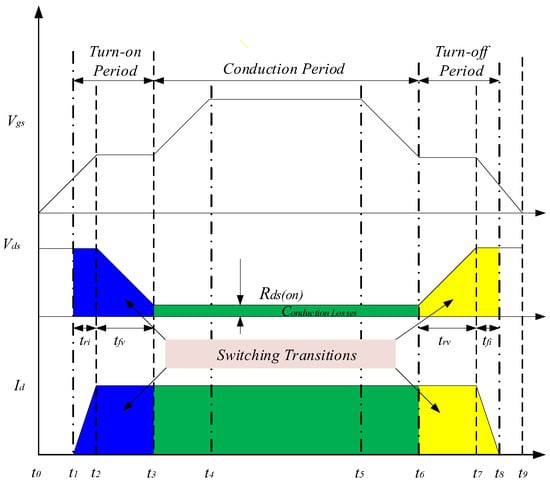
Figure 10.
A figure of ideal switching transitions showing switching transition and conduction loss.
2.4. Modeling of the Switching Losses
When quantifying the power losses, the switching loss of the diode is usually neglected, since it is much smaller in comparison with the switching loss of both devices [41]. Although different switching devices are used in the evaluation, the loss computation methodology is identical. The loss prediction under a similar setup provides an accurate comparison of losses and performance, taking temperature effects into account. It was observed that the total switching energy losses in Si and SiC MOSFETs primarily consist of the turn-on () and turn-off () dissipated energy. These two added together give the total switching energy loss expressed as Equation (1):
2.5. Comparison of Junction Temperature Variation on Si and SiC Devices
The temperature influence is significant on the switching transitions for both the Si and SiC devices. The gate threshold voltage, device carrier mobility, and transconductance, among others. Figure 11 is a clear illustration that the temperature has a relatively obvious influence on the devices in question during the turn-off events. Furthermore, it is observed that the rising time of the drain–source voltage increases with an increase in the temperature (25–C), being more significant in Si devices as seen in Figure 11D, compared to SiC devices observed in Figure 11B, and so does the decay time of the current as observed in Figure 11A,C, with it being more pronounced in Si devices than SiC, respectively. Figure 11C shows the tail current clearly. Additionally, during the turn-on process, the voltage decay time and the current rise time decrease as the temperature increases. Ideally, for this work, turn-off variations were preferred for detailed evaluation as they contain the tail current; similarly, variations in turn-on energy loss could also have been performed, though the tail current would not have been shown.
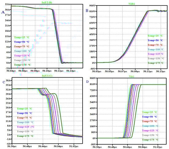
Figure 11.
Analytical switching waveforms showing turn-off characteristics of Si and SiC MOSFET with temperature variations. (A) SiC turn-off current, (B) SiC turn-off voltage, (C) Si turn-off current, (D) Si turn-off voltage.
Figure 12a,b show the behavior of the threshold voltage with temperature increase for Si and SiC devices, respectively. The extraction of the variation in threshold voltage from the manufacturer’s modules followed the data sheets test conditions for recommended drain current, which is then extrapolated to the whole range of temperature from −50 °C to 150 °C. In this case, where the average is given as 6V at = 120.7 mA, a −4/15 V gate source voltage is used. The +15 V provides a strong drive that is way beyond the maximum threshold voltage of the device to ensure low conduction losses. In this device, the minimum voltage is −5 V, and the supplied gate voltage during the off state is −4 V, which is way below the pin level. This ensures total prevention from spurious triggering, which could accidentally switch on the switch, thus providing a degree of inherent noise immunity. When plotting vs. temperature, the curve has a negative coefficient, meaning the threshold voltage decreases as the junction temperature increases. Thus, the graph has an almost linear curve with a negative slope. From the figures, it is clear that the gate-emitter threshold voltage decreases from −50 V to 150 V, i.e., from 6.16 V to 4.52 V, which is approximately 8.2 mV/°C. Similarly, the threshold voltage vs. temperature curve of the SiC MOSFET showed a decrease in threshold voltage almost linearly with increasing temperature; thus, at higher temperatures, less threshold voltage is required to turn on the device. This is due to the consequent decrease in carrier mobility and intrinsic carrier concentration with temperature increase, subsequently reducing the required gate voltage. From Equation (4), the gate threshold voltage rate of change is . The negative temperature coefficient of improves the static thermal stability as the device naturally limits currents when the temperature is elevated. Table 5 shows the data trend for the SiC and Si threshold voltage as the temperature increases.
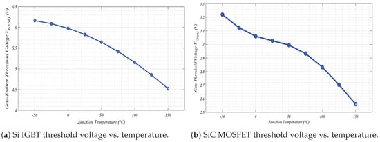
Figure 12.
Threshold voltage variation with temperature for (a) Si IGBT and (b) SiC MOSFET.
Table 5.
Variation of threshold voltage with temperature for SiC MOSFET and Si IGBT devices.
With a dc-link voltage of 800 V, the switching energy loss of Si IGBT and SiC MOSFET under different junction temperatures was computed and illustrated in Figure 13a,b, respectively. It was observed that there is a linear trend across all temperatures. In higher currents, a great energy is stored in the device’s magnetic components and capacitance, which is dissipated, translating to higher energy loss. Since there is a long current tail in Si IGBT during the turn-off process, the energy dissipation is higher. As observed, at 4A, 1.2 mJ is lost at , with an energy loss of 3.3 mJ lost at in the Si device. Comparatively, the energy loss in the SiC device increases with an increase in drain current; however, a slight variation was observed with temperature variations, as shown in Table 6.
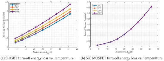
Figure 13.
Turn-off energy loss variation with temperature for (a) Si IGBT and (b) SiC MOSFET.
Table 6.
Variation of threshold voltage with temperature for Si IGBT and SiC MOSFET devices.
Temperature variations, as seen in Figure 14a, significantly influence the rate of change in drain current . However, in opposite ways. As temperature increases, the turn-on rate of decreases, whereas the rate of change in drain current increases during the turn-off [42,43]. This is because the channel mobility reduces with temperature during turn-on, and the channel resistance increases during turn-off, reducing the mobility. Finally, Figure 14b illustrates the turn-on and turn-off energy loss. As expected, the energy losses in the Si device are higher than it they are the SiC MOSFET.
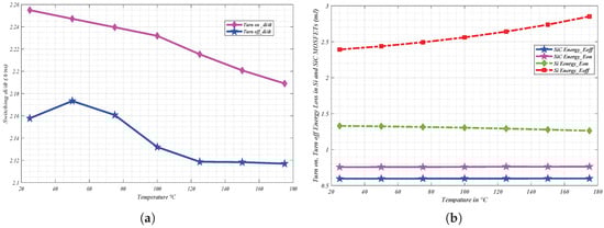
Figure 14.
SiC MOSFET and comparison analysis of Si and SiC turn-on and turn-off energy loss at different temperatures [°C]. (a) SiC MOSFET turn-on (turn-off) switching . (b) Si IGBT and SiC MOSFET turn-off energy loss at different temperatures.
3. Comparison of Si and SiC MOSFET Different Parameters
3.1. Dynamic Comparision of SiC MOSFET and Si IGBT
The switching energy loss was quantified for the Si and SiC MOSFETs under the same conditions and with similar parameters as much as possible. Figure 15 shows a comparison between the SiC and Si energy loss across different drain currents, whereas Figure 16 shows the switching energy loss during the turn-off for the Si and SiC MOSFETs. Amongst the ones quantified, i.e., from = 200 V to 1200 V and = 4–36 A, for demonstration purposes, only at = 600 V and 1000 V were plotted against the . It is observed that the energy loss for Si is consistently higher than for SiC at all current levels. The trend shows a near-linear increase in energy loss as the drain current increases, with SiC exhibiting a significantly lower loss than Si. For instance, at = 600 V and , SiC energy loss is 0.5185 mJ against Si’s 2.4173 mJ, highlighting a reduction when using the SiC MOSFETs. The trend continues until 1000 V operation, with SiC maintaining lower losses (0.93 mJ vs. 5.95 mJ), which reinforces the great advantage of SiC in higher power applications. The total energy loss shown in Figure 17 affirms that even after the summation of the turn-on and turn-off, the SiC energy loss remains significantly lower. At lower current, the SiC MOSFET has a lower conduction loss compared to the Si IGBT; this is because of the pure Ohmic characteristics of the SiC MOSFETs. This shows that the SiC is more preferable in comparison with Si. The converse is true in IGBT due to the presence of the current tail, which increases the switching time, causing non-linear behavior during the turn-off and consequently increased turn-off losses.
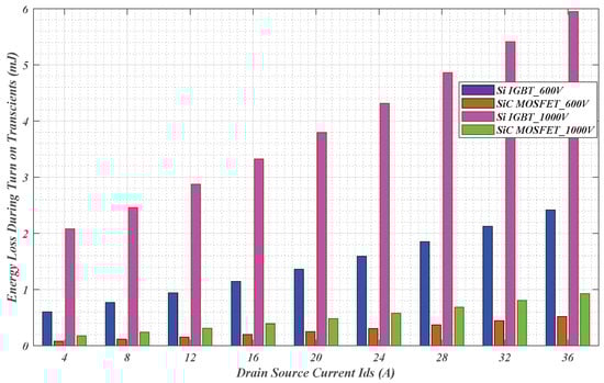
Figure 15.
Comparison analysis of turn-on energy loss of Si and SiC MOSFETs at 600 V and 1000 V operating voltages.
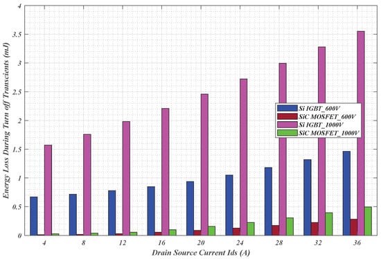
Figure 16.
Comparison analysis of turn-off energy loss of Si and SiC MOSFETs at 600 V and 1000 V operating voltages.
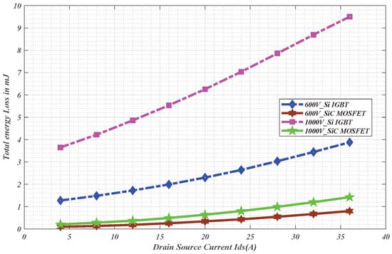
Figure 17.
Comparison analysis of total turn-on and turn-off energy loss of Si and SiC MOSFETs at 600 V and 1000 V operating voltages.
The characterized switching power loss during turn-on is illustrated in Figure 18, showing a consistent power loss increase as current increases. Additionally, SiC consistently achieves lower values of turn-on power dissipation. Figure 19 and Figure 20 reaffirm this observation. As Figure 19 indicates, the comparison of the power loss between Si and SiC shows that Si power loss remains higher than SiC. The total power loss from the two devices, which is shown by Figure 20, exhibits that the cumulative total loss in SiC MOSFETs is lower than the Si counterparts across the whole operation range, whereas Table 7a,b details the segregated switching power loss and condition power loss for the devices under texts, at 600V and 800V respectively. Table 8a,b shows in detail the total loss for Si and SiC devices in the whole load current range as well as the respective efficiency.
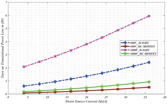
Figure 18.
The turn-on transition power loss of the switch drain source current .
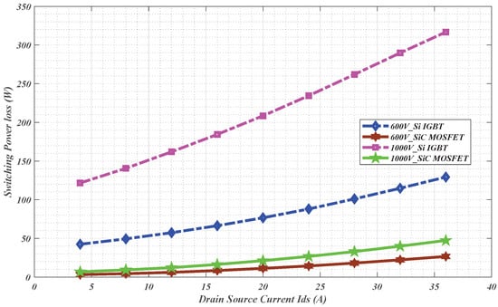
Figure 19.
Switching power loss comparison in SiC and Si IGBT.
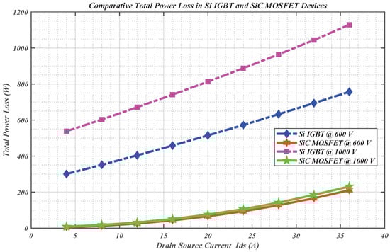
Figure 20.
The curves of total switching power loss dissipated during turn-on and turn-off transitions in SiC MOSFET and Si IGBT under varying drain–source current.
Table 7.
Comparative switching and conduction losses in Si and SiC devices.
Table 8.
Comparative performance of Si IGBT and SiC MOSFET devices under different load currents and voltages.
3.2. Si IGBT and SiC MOSFET Efficiency Comparison
The total cumulative loss in each device forms a significant part of determining the efficiency achieved. The lower the losses, the higher the efficiency. It has been seen that the SiC MOSFETs consistently had lower losses than the Si IGBT; consequently, the efficiency of the SiC, as seen in Figure 21, is higher. It was observed that at lower currents, the losses are significantly lower and increase as the current increases. In tandem with this, the efficiency is higher at lower current, resulting from lower cumulative losses for the same power output. From the figure, the efficiency of 99.78% and 99.03% was observed at = 4 A and = 36 A, respectively, for a SiC MOSFET at 600 V. Comparatively, efficiency of 88.87% and 96.62% was observed at = 4 A and = 36 A, respectively, for a Si IGBT at 600V. Notably, whilst the switching losses increase with the increase in voltages, they do so at a significantly smaller rate at high voltages.
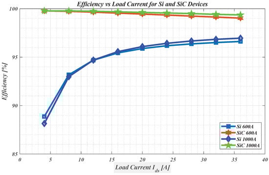
Figure 21.
The efficiency comparison between the Si and SiC MOSFET when the drain–source current is varied.
4. Conclusions
This study presented a comprehensive evaluation of the dynamic performance characteristics of Silicon-Insulated Gate Bipolar Transistors (Si IGBTs) and Silicon Carbide Metal-Oxide-Semiconductor Field-Effect Transistors (SiC MOSFETs) under various operating parameters for high-frequency DC-DC converter applications. The switching behaviors were analyzed, and switching losses were analyzed as a function of load current, gate resistance, and DC-bus voltage. Notably, switching losses increase with an increase in gate resistance. The analysis done indicates that the SiC-based devices have superior and better performance in comparison with the Si-based devices. This is attributed to Si IGBTs’ significant tail current and slower switching behavior, which contributes to higher turn-off loss, hence limiting their stability at elevated frequencies, whereas the SiC MOSFETs’ superior performance was noted, resulting from reduced energy loss, the fast turn-on and turn-off making them better suited for higher frequencies, albeit with higher EMI sensitivity. The SiC demonstrated high efficiency in comparison with Si. The study offers invaluable insights into the trade-off involved in selecting semiconductor devices for power electronic systems, particularly under high-frequency switching conditions. The SiC MOSFET showed lower losses when compared with Si modules at the same test parameters. Moreover, lower voltage overshoots were observed, and this allowed a further increase in the dc-link voltage levels. This implies that the SiC can replace the Si IGBT even at a higher voltage class. It was observed that the turn-on loss in SiC is lower than in Si, even when the ringing was similar. The higher losses in Si are attributed to the higher of the Si diode. These findings provide valuable insights that govern device selection for high efficiency and high frequency, and confirm that the SiC can be used to retrofit Si devices even for higher voltages.
Author Contributions
Conceptualization, J.M.K. and M.A.; methodology, J.M.K.; software, J.M.K.; validation, J.M.K.; formal analysis, J.M.K.; investigation, J.M.K.; resources, J.M.K. and M.A.; writing—original draft J.M.K.; writing—review and editing M.A.; visualization, M.A.; supervision M.A. All authors have read and agreed to the published version of the manuscript.
Funding
This research received no external funding.
Data Availability Statement
The original contributions presented in this study are included in the article. Further inquiries can be directed to the corresponding author.
Conflicts of Interest
The authors declare no conflicts of interest.
Abbreviations
The following abbreviations are used in this manuscript:
| DC | Direct Current |
| DPT | Double Pulse Test |
| DUT | Device Under Test |
| EMI | Electromagnetic Interference |
| HFT | High Frequency Transformer |
| SCSOA | Short-Circuit Safe Operation Area |
| Si | Silicon |
| SiC MOSFET | Silicon Carbide Metal-Oxide Semiconductor Field-Effect Transistor |
| SiC SBD | Silicon Carbide Schottky Barrier Diode |
| WBG | Wide Band Gap |
| ZVS | Zero Voltage Switching |
References
- Alam, M.; Kumar, K.; Dutta, V. Comparative Efficiency Analysis for Silicon, Silicon Carbide MOSFETs and IGBT Device for DC–DC Boost Converter. SN Appl. Sci. 2019, 1, 1700. [Google Scholar] [CrossRef]
- Han, D.; Noppakunkajorn, J.; Sarlioglu, B. Efficiency Comparison of SiC and Si-based Bidirectional DC-DC Converters. In Proceedings of the 2013 IEEE Transportation Electrification Conference and Expo (ITEC), Detroit, MI, USA, 16–19 June 2013; pp. 1–7. [Google Scholar] [CrossRef]
- Zhao, B.; Song, Q.; Liu, W. Experimental Comparison of Isolated Bidirectional DC–DC Converters Based on All-Si and All-SiC Power Devices for Next-Generation Power Conversion Application. IEEE Trans. Ind. Electron. 2014, 61, 1389–1393. [Google Scholar] [CrossRef]
- Wang, W.; Song, Q.; Zhang, S.; Li, Y.; Ahmad, M.; Gong, Y. The Loss Analysis and Efficiency Optimization of Power Inverter Based on SiC MOSFETs Under the High-Switching Frequency. IEEE Trans. Ind. Appl. 2021, 57, 1521–1534. [Google Scholar] [CrossRef]
- Marzoughi, A.; Burgos, R.; Boroyevich, D. Characterization and Performance Evaluation of the State-of-the-Art 3.3 kV 30 A Full-SiC MOSFETs. IEEE Trans. Ind. Appl. 2019, 55, 575–583. [Google Scholar] [CrossRef]
- Wang, G.; Wang, F.; Magai, G.; Lei, Y.; Huang, A.; Das, M. Performance Comparison of 1200V 100A SiC MOSFET and 1200V 100A Silicon IGBT. In Proceedings of the 2013 IEEE Energy Conversion Congress and Exposition, Denver, CO, USA, 15–19 September 2013. [Google Scholar] [CrossRef]
- Yin, S.; Tseng, K.J.; Simanjorang, R.; Tu, P. Experimental Comparison of High-Speed Gate Driver Design for 1.2-kV/120-A Si IGBT and SiC MOSFET Modules. IET Power Electron. 2017, 10, 979–986. [Google Scholar] [CrossRef]
- She, X.; Losee, P.; Hu, H.; Earls, W.; Datta, R. Performance Evaluation of 1.5 kV Solar Inverter With 2.5 kV Silicon Carbide MOSFET. IEEE Trans. Ind. Appl. 2019, 55, 7726–7735. [Google Scholar] [CrossRef]
- Hazra, S.; De, A.; Cheng, L.; Palmour, J.; Schupbach, M.; Hull, B.; Allen, S.; Bhattacharya, S. High Switching Performance of 1700V, 50A SiC Power MOSFET over Si IGBT/BiMOSFET for Advanced Power Conversion Applications. IEEE Trans. Power Electron. 2015, 31, 4742–4754. [Google Scholar] [CrossRef]
- Albanna, A.; Malburg, A.; Anwar, M.; Guta, A.; Tiwari, N. Performance Comparison and Device Analysis Between Si IGBT and SiC MOSFET. In Proceedings of the 2016 IEEE Transportation Electrification Conference and Expo (ITEC), Dearborn, MI, USA, 27–29 June 2016; pp. 1–6. [Google Scholar] [CrossRef]
- Rizzoli, G.; Mengoni, M.; Zarri, L.; Tani, A.; Serra, G.; Casadei, D. Comparative Experimental Evaluation of Zero-Voltage-Switching Si Inverters and Hard-Switching Si and SiC Inverters. IEEE J. Emerg. Sel. Top. Power Electron. 2019, 7, 515–527. [Google Scholar] [CrossRef]
- Ding, X.; Du, M.; Zhou, T.; Guo, H.; Zhang, C. Comprehensive Comparison Between Silicon Carbide MOSFETs and Silicon IGBTs Based Traction Systems for Electric Vehicles. Appl. Energy 2017, 194, 626–634. [Google Scholar] [CrossRef]
- Hazra, S.; De, A.; Bhattacharya, S.; Cheng, L.; Palmour, J.; Schupbach, M.; Hull, B.; Allen, S. High switching Performance of 1.7kV, 50A SiC Power MOSFET Over Si IGBT for Advanced Power Conversion Applications. In Proceedings of the 2014 International Power Electronics Conference (IPEC-Hiroshima 2014–ECCE ASIA), Hiroshima, Japan, 18–21 May 2014; pp. 3447–3454. [Google Scholar] [CrossRef]
- Jahdi, S.; Alatise, O.; Ortiz Gonzalez, J.A.; Bonyadi, R.; Ran, L.; Mawby, P. Temperature and Switching Rate Dependence of Crosstalk in Si-IGBT and SiC Power Modules. IEEE Trans. Ind. Electron. 2016, 63, 849–863. [Google Scholar] [CrossRef]
- Allca-Pekarovic, A.; Kollmeyer, P.J.; Mahvelatishamsabadi, P.; Mirfakhrai, T.; Naghshtabrizi, P.; Emadi, A. Comparison of IGBT and SiC Inverter Loss for 400V and 800V DC Bus Electric Vehicle Drivetrains. In Proceedings of the 2020 IEEE Energy Conversion Congress and Exposition (ECCE), Detroit, MI, USA, 11–15 October 2020; pp. 6338–6344. [Google Scholar] [CrossRef]
- Zhou, W.; Yuan, X. Experimental Evaluation of SiC MOSFETs in Comparison to Si IGBTs in a Soft-Switching Converter. IEEE Trans. Ind. Appl. 2020, 56, 5108–5118. [Google Scholar] [CrossRef]
- Nawaz, M.; Ilves, K. On the comparative assessment of 1.7 kV, 300 a full SiC-MOSFET and Si-IGBT power modules. In Proceedings of the 2016 IEEE Applied Power Electronics Conference and Exposition (APEC), Long Beach, CA, USA, 20–24 March 2016; pp. 276–282. [Google Scholar] [CrossRef]
- Shah, F.M.; Xiao, H.M.; Li, R.; Awais, M.; Zhou, G.; Bitew, G.T. Comparative Performance Evaluation of Temperature Dependent Characteristics and Power Converter Using GaN, SiC and Si Power Devices. In Proceedings of the 2018 IEEE 12th International Conference on Compatibility, Power Electronics and Power Engineering (CPE-POWERENG 2018), Doha, Qatar, 10–12 April 2018; pp. 1–7. [Google Scholar] [CrossRef]
- Li, Y.; ul Hassan, M.; Mirza, A.B.; Xie, Y.; Deng, S.; Vala, S.S.; Luo, F.; Feng, X.; Narumanchi, S.V.J.; Flicker, J.D. State-of-the-Art Medium- and High-Voltage Silicon Carbide Power Modules, Challenges and Mitigation Techniques: A Review. IEEE Trans. Compon. Packag. Manuf. Technol. 2024, 14, 2177–2195. [Google Scholar] [CrossRef]
- Perdikakis, W.; Scott, M.J.; Yost, K.J.; Kitzmiller, C.; Hall, B.; Sheets, K.A. Comparison of Si and SiC EMI and Efficiency in a Two-Level Aerospace Motor Drive Application. IEEE Trans. Transp. Electrif. 2020, 6, 1401–1411. [Google Scholar] [CrossRef]
- Moaz, T.; Rajagopal, N.; DiMarino, C.; Fish, M. EMI Mitigation for SiC MOSFET Power Modules Using Integrated Common-Mode Screen. IEEE Open J. Power Electron. 2023, 4, 873–886. [Google Scholar] [CrossRef]
- Kinyua, J.M.; Aoki, M. Modeling of RC Snubber, Ferrite Bead and Gate Drive Impedance for Optimal EMI Suppression and Switching Loss Trade-Off in SiC MOSFET Power Converters. In Proceedings of the 2025 International Conference on Sustainable Technology and Engineering (i-COSTE), Washington University of Science and Technology, Alexandria, VA, USA, 2–4 December 2025. [Google Scholar]
- Zhang, M.; Li, H.; Yang, Z.; Zhao, S.; Wang, X.; Ding, L. Short Circuit Protection of Silicon Carbide MOSFETs: Challenges, Methods, and Prospects. IEEE Trans. Power Electron. 2024, 39, 13081–13095. [Google Scholar] [CrossRef]
- Ye, J.; Wang, M.; Cui, S.; Zhang, C.; Li, L. An Improved Crosstalk Suppression Driver Topology for SiC MOSFET With Fast Switching Transient in the Phase-Leg Configuration. IEEE Trans. Power Electron. 2025, 40, 8448–8467. [Google Scholar] [CrossRef]
- Kinyua, J.M.; Aoki, M. SiC MOSFET Switching Dynamics and Power Conversion Loss Characterization Under Parametric Variations. Energies 2025, 18, 6264. [Google Scholar] [CrossRef]
- Li, Q.; Yang, Y.; Wen, Y.; Zhang, G.; Xing, W. Active Gate Driver With the Independent Suppression of Overshoot and Oscillation for SiC MOSFET Modules. IEEE Trans. Ind. Electron. 2025, 72, 2325–2335. [Google Scholar] [CrossRef]
- Du, Y.; Lu, K.; Zhang, B.; Iqbal, A.; Wang, S.; Qiu, J.; Liu, K.; Zhao, H.; Long, T.; Jiang, C. Reducing Near-Field Magnetic Radiation and Parasitic Inductance in SiC Half-Bridge Modules via Optimized Shielding Design. IEEE Trans. Power Electron. 2025, 40, 12003–12010. [Google Scholar] [CrossRef]
- ROHM Semiconductor. “Power Device Catalog, Ver. 7.0”, 2024. Available online: https://fscdn.rohm.com/en/products/databook/catalog/common/P_PowerDevice_EN.pdf (accessed on 1 April 2025).
- Mocevic, S.; Wang, J.; Burgos, R.; Boroyevich, D.; Jaksic, M.; Stancu, C.; Peaslee, B. Comparison and Discussion on Shortcircuit Protections for Silicon-Carbide MOSFET Modules: Desaturation Versus Rogowski Switch-Current Sensor. IEEE Trans. Ind. Appl. 2020, 56, 2880–2893. [Google Scholar] [CrossRef]
- Fuentes, C.D.; Kouro, S.; Bernet, S. Comparison of 1700V SiC-MOSFET and Si-IGBT Modules Under Identical Test Setup Conditions. IEEE Trans. Ind. Appl. 2019, 55, 7765–7775. [Google Scholar] [CrossRef]
- Kinyua, J.M.; Aoki, M. Investigating the Parasitic Elements Sensitivity on Switching Transient in SiC MOSFET for High Frequency Power Conversion. In Proceedings of the 2025 IEEE PES/IAS PowerAfrica Conference, Cairo, Egypt, 28 September–2 October 2025. [Google Scholar]
- Arribas, A.P.; Shang, F.; Krishnamurthy, M.; Shenai, K. Simple and Accurate Circuit Simulation Model for SiC Power MOSFETs. IEEE Trans. Electron Devices 2015, 62, 449–457. [Google Scholar] [CrossRef]
- Silva, D.R.F.; Guerreiro, J.F.; Spejo, L.B.; Puydinger Dos Santos, M.V. Development of a Double Pulse Test Plataform for Switching Loss Investigation in Emerging SiC MOSFET Technology. In Proceedings of the 2024 38th Symposium on Microelectronics Technology and Devices (SBMicro), Joao Pessoa, Brazil, 2–6 September 2024; pp. 1–4. [Google Scholar] [CrossRef]
- Kinyua, J.M.; Aoki, M. Multi-Parametric Dynamic Performance Evaluation of Si IGBT and SiC MOSFETs for High-Frequency DC-DC Converter Applications. In Proceedings of the IEEE PES/IAS Power Africa Conference, Cairo, Egypt, 28 September– 2 October 2025. [Google Scholar]
- Vechalapu, K.; Bhattacharya, S.; Van Brunt, E.; Ryu, S.H.; Grider, D.; Palmour, J.W. Comparative Evaluation of 15-kV SiC MOSFET and 15-kV SiC IGBT for Medium-Voltage Converter Under the Same dv/dt Conditions. IEEE J. Emerg. Sel. Top. Power Electron. 2017, 5, 469–489. [Google Scholar] [CrossRef]
- Marz, A.; Horff, R.; Helsper, M.; Bakran, M.M. Requirements to Change from IGBT to Full SiC Modules in an On-board Railway Power Supply. In Proceedings of the 2015 17th European Conference on Power Electronics and Applications (EPE’15 ECCE-Europe), Geneva, Switzerland, 8–10 September 2015; pp. 1–10. [Google Scholar] [CrossRef]
- Wolfspeed, Inc. C3M0075120D-A Silicon Carbide Power MOSFET C3M MOSFET Technology N-Channel Enhancement Mode. Available online: https://assets.wolfspeed.com/uploads/2024/01/Wolfspeed_C3M0075120D-A_data_sheet.pdf (accessed on 3 April 2025).
- ROHM Semiconductor, Inc. “RGC80TSX8R 1800V 40A Field Stop Trench IGBT”. 2019. Available online: https://www.rohm.com/products/igbt/field-stop-trench-igbt/rgc80tsx8r-product (accessed on 17 April 2025).
- Tiwari, S.; Midtgard, O.M.; Undeland, T.M. Comparative Evaluation of a Commercially Available 1.2 kV SiC MOSFET Module and a 1.2 kV Si IGBT Module. In Proceedings of the IECON 2016–42nd Annual Conference of the IEEE Industrial Electronics Society, Florence, Italy, 23–26 October 2016; pp. 1093–1098. [Google Scholar] [CrossRef]
- Zhang, L.; Yuan, X.; Wu, X.; Shi, C.; Zhang, J.; Zhang, Y. Performance Evaluation of High-Power SiC MOSFET Modules in Comparison to Si IGBT Modules. IEEE Trans. Power Electron. 2019, 34, 1181–1196. [Google Scholar] [CrossRef]
- Ding, X.; Du, M.; Zhou, T.; Guo, H.; Zhang, C.; Chen, F. Comprehensive Comparison between SiC-MOSFETs and Si-IGBTs Based Electric Vehicle Traction Systems under Low Speed and Light Load. Energy Procedia 2016, 88, 991–997. [Google Scholar] [CrossRef]
- Peng, K.; Eskandari, S.; Santi, E. Characterization and Modeling of SiC MOSFET Body Diode. In Proceedings of the 2016 IEEE Applied Power Electronics Conference and Exposition (APEC), Long Beach, CA, USA, 20–24 March 2016. [Google Scholar] [CrossRef]
- Liao, X.; Li, H.; Hu, Y.; Huang, Z.; Song, E.; Xiao, H. Analysis of SiC MOSFET dI/dt and its Temperature Dependence. In Proceedings of the IECON 2017–43rd Annual Conference of the IEEE Industrial Electronics Society, Beijing, China, 29 October–1 November 2017; pp. 864–869. [Google Scholar] [CrossRef]


Disclaimer/Publisher’s Note: The statements, opinions and data contained in all publications are solely those of the individual author(s) and contributor(s) and not of MDPI and/or the editor(s). MDPI and/or the editor(s) disclaim responsibility for any injury to people or property resulting from any ideas, methods, instructions or products referred to in the content. |
© 2025 by the authors. Licensee MDPI, Basel, Switzerland. This article is an open access article distributed under the terms and conditions of the Creative Commons Attribution (CC BY) license (https://creativecommons.org/licenses/by/4.0/).