Abstract
This paper presents the results of research on the effect of temperature on damage processes occurring in power MOSFETs. The impact of changes in the activation energy of selected mechanisms initiating the damage process in power MOSFETs during continuous operation on their lifetime is analyzed. Computer analyses and experiments illustrating the effect of transistor switching frequency on time to failure are also conducted. The impact of the relationship between the transistor’s thermal time constants and its switching period on lifetime is assessed. The effect of the transistor’s switching frequency on its junction temperature swing and average value is also assessed. Recommendations for designers of systems using these transistors are formulated to improve their reliability.
1. Introduction
A significant issue for users of electrical devices is their reliability. This can be expressed as the device’s lifetime or the expected operating time to failure [1]. A short lifetime can be a reason for the device’s lack of market success, but it also determines the interval between service activities. This parameter describes the expected number of operating hours to failure under steady-state operating conditions of electronic devices. Lifetime is typically determined for steady-state operating conditions of a device operating under direct current loads [2].
The lifetime of a device is related both to the lifetime of the components used in its construction and to the degradation time of soldered joints. The lifetime value of an electronic component depends, among other things, on its junction temperature [3,4].
To verify the strength of solder joints and their degradation during device operation, electronic module tests are performed using appropriately determined thermal cycles. As presented in [5,6], solder joints are subject to stresses resulting from thermal cycling and constant elevated temperatures (from 40 °C to 70 °C) during the operation of electronic components. This leads to thermomechanical fatigue and the formation of intermetallic compounds. In the tests described in the cited paper for photovoltaic modules, the strength of solder joints at operating temperatures of 85 °C, 95 °C, and 105 °C was examined in 15 min cycles [5,7,8].
The cited papers show that the temperature at the leads of electronic components has a significant impact on the lifetime of a soldered joint [3,9]. The strength of such joints is also related to the size of the component. Paper [4] presents a graph showing the dependence of the risk of soldered joint damage on the size of the soldered component and the temperature. The graph shows that at temperatures below 85 °C, the risk of damage is very low, while above 105 °C, it is unacceptably high. In the temperature range from 85 to 105 °C, the risk of damage increases with increasing component surface area. The risk of solder joint damage decreases with decreasing temperature and increasing component size. This dependence results from the increase in the thermal capacity of the component with increasing size [4].
In [10], a novel method for bond wire lift-off failure prediction in IGBTs is presented. This method takes into account the non-uniform temperature distribution on the chip during crack propagation at the interface, which allows for a smaller prediction error. It was shown that the maximum number of power cycles depends on the crack length and the fluctuations of the transistor junction temperature.
According to the Arrhenius formula [11], the operating time τ until component failure at temperature Tj is described by the formula [4,11]:
where Ea is the activation energy of the damage process, k is the Boltzmann constant, and τ0 is the lifetime of the element operating at temperature T0.
From the form of Formula (1), it follows that the change in the device lifetime at a constant temperature increase strongly depends on the activation energy of the damage process. The energy values Ea for different damage processes can differ up to tenfold [11].
For power electronics components, the natural operating mode is switching mode, with alternating time intervals when the device is on and time intervals when it is off. The duration of these intervals can vary widely depending on the application of the devices under consideration [12].
Every power electronic device contains transistors that act as power electronic switches [13]. As current flows through these transistors, electrical energy is dissipated within them and converted into heat. This heat causes the transistors’ junction temperature to increase due to self-heating phenomena [14,15]. During turn-on and turn-off cycles, the power dissipated within a transistor is significantly greater than during off cycles [16,17]. Therefore, the junction temperature of a transistor changes during device operation, increasing during on-cycle operation and decreasing during off-cycle operation. This leads to thermal cycles of transistor heating and cooling.
The junction temperature of an electronic component Tj is the sum of the ambient temperature Ta, and the increase in this temperature ΔT caused by the self-heating phenomenon [18,19]. The value of ΔT depends on the power p lost in this component and the transient thermal impedance Zth(t), which characterizes the efficiency of dissipating the generated heat to the surroundings [20]. As it results from, among others, papers [21,22], changes in the value of Tj caused by the self-heating phenomenon have a significant impact on the lifetime of the components.
Thermal processes occurring in semiconductor devices depend on the parameters of the power dissipation p(t) and the design of their cooling system, the properties of which are described by the transient thermal impedance Zth(t). According to the classical compact thermal model, the time course of the transistor junction temperature can be described by the formula [18,23]:
where Ta is the ambient temperature and Z′th(t) is the time derivative of the transient thermal impedance Zth(t), which is typically approximated by a sum of exponential functions according to the formula [18]:
In Formula (3), Rth denotes the thermal resistance, and ai are weighting factors associated with individual thermal time constants τthi, the number of which is equal to N. Formula (3) characterizes the heat flow from the semiconductor chip to the surroundings, and the values of the parameters appearing in this formula are determined by all components of the heat flow path. These include, among others, the transistor case, the printed circuit board mosaic, the thermal interface between the transistor case and the heat sink, the heat sink and its cooling system [24,25,26].
Due to differences in the properties of structural materials and the dimensions of individual components, the values of individual thermal time constants τthi vary by up to several orders of magnitude [20,25,27,28]. These differences cause different values of the junction temperature amplitude to be observed depending on the frequency of the p(t) waveform and its amplitude. It can be expected that the period of thermal cycling (corresponding to the period of active thermal cycling) will influence the operating time of the tested component until failure. This hypothesis was confirmed for power LEDs in [29], but it has not yet been tested for power electronic switches.
The aim of this paper is to investigate the influence of two factors on the lifetime of power MOSFETs. The first is the activation energy of the failure process, and the second is the relationship between the switching period and the thermal time constants of this transistor. The study was conducted for the IPB090N06N3G transistor [30], belonging to the OptiMOS3 transistor family manufactured by Infineon Technologies (Neubiberg, Germany).
Section 2 describes the measurement setup and the measurement procedure. Section 3 contains the measurement results obtained for the tested transistors. Section 4 presents the results of calculations illustrating the effect of the activation energy and the junction temperature of the tested transistor on the change in transistor lifetime.
2. Measurement Method and Set-Ups
To perform the experimental part of the planned tests, it was necessary to use two measurement set-ups. The first one allows for the measurement of the transient thermal impedance Zth(t) of the tested transistor using an indirect electrical method [25,31]. A diagram of this set-up is shown in Figure 1. The second measurement set-up is designed to perform reliability tests during the thermal cycling test. A diagram of this set-up is shown in Figure 2.
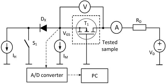
Figure 1.
Transient thermal impedance measurement set-ups.
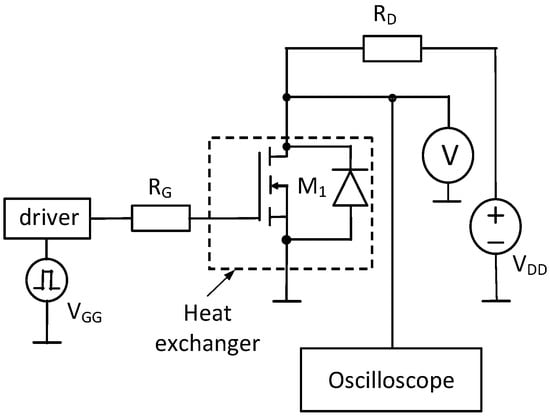
Figure 2.
Power cycling measurement set-up.
In the measurement set-up shown in Figure 1, the tested transistor T1 operates in a common gate configuration. This transistor is located inside an isothermal chamber. The drain circuit of this transistor is powered from a voltage source VD through a resistor RD. The source part of the circuit contains two current sources IM and IH, a diode Dx, and a switch S1.
The Zth(t) measurement is performed using an indirect electrical method, in which the gate-source voltage VGS at a fixed drain current value equal to IM is used as a thermally sensitive parameter. The measurement process comprises three stages: calibration, heating the transistor to a steady state, and cooling the transistor, during which the time course of VGS(t) is recorded. After the measurement is completed, the Zth(t) course is determined based on the measured VGS(t) course. This process is described in detail, among others, in [19,25].
The VGS(t) voltage waveform is recorded using the A/D converter module and a PC. A voltmeter and an ammeter are used to measure the VDS voltage and IH current during the heating of the tested transistor. Switch S1 is closed during calibration and cooling of the transistor and open during the heating period.
The set-up shown in Figure 2 includes the tested transistor M1 operating in a switching system with a resistive load RD. The drain circuit is powered by a VDD power supply operating as a current source of the value 50 A (when the tested transistor is turned on) or a DC voltage source of the value 10 V (when the transistor is turned off). Voltage source VDD is realized by parallel connecting the power supply GWInstek PSB-2800LS (Good Will Instrument Co., New Taipei City, Taiwan) with booster GWInstek PSB-2800L (Good Will Instrument Co., New Taipei City, Taiwan). The transistor gate is controlled by a rectangular pulse train from the VGG function generator of the type Rigol DG1022 (RIGOL Technologies, Co., Suzhou New District, China) via the gate driver IR2125 (Infineon Technologies AG, Neubiberg, Germany) and the resistor RG of the resistance 220 Ω to reduce the time derivative of the gate current.
The voltmeter cooperates with a computer that records long-term changes in VDS voltage across the transistor with a sampling frequency equal to 1 Hz to monitor the degradation of the tested device. Based on the recorded waveform VDS(t), the time at which the tested transistor was damaged and the number of thermal cycles that preceded the damage were determined.
The oscilloscope is used to measure the VDS(t) voltage waveform with a high sampling frequency. From this waveform, the power p dissipated in the tested transistor is determined, assuming a zero value of the drain current when the transistor is turned off and a constant value of this current when it is turned on.
3. Results of Measurements
The IPB090N06N3G (Infineon Technologies AG, Neubiberg, Germany) power MOSFET manufactured by Infineon was selected for testing. This transistor belongs to the OptiMOS3 power transistor family, designed for use in synchronous rectifiers, controllers, and switched-mode power supplies. According to the manufacturer’s data [30], this transistor has a maximum allowable VDS voltage of 60 V and a maximum allowable drain current ID of 50 A. The RON resistance for this transistor is 9 mΩ. This resistance value increases by 50% with a temperature increase of 100 °C. The permissible power at a case temperature of 25 °C is 71 W, but at a temperature of 70 °C it decreases to 60 W. The thermal resistance of the tested transistor between the junction and the case does not exceed 1.6 K/W [30].
The transistor under test is mounted in a TO-263 case and soldered to the MCPCB board, shown in Figure 3, using SAC0307 paste. A thermal interface is provided between the metal part of this board and the heat exchanger, ensuring good thermal contact between these components of the heat flow path. The transistor under test is mounted on an aluminum heat exchanger through which a coolant flows at a fixed temperature Ta = 70 °C. This coolant is pumped by ThermoFisher (Waltham, MA, USA) Haase AC200 liquid cooling system [32]. The MCPCB board is screwed to the heat exchanger with an M4 screw using a torque of 0.6 Nm.
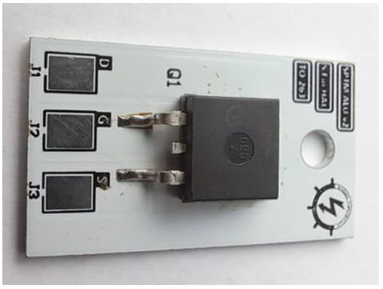
Figure 3.
View of the tested transistor assembled on the MCPCB.
3.1. Measurements of Transient Thermal Impedance
To determine the time course of the junction temperature of the tested transistor during the aging test, it was necessary to first measure the transient thermal impedance Zth(t) of this transistor mounted on a heat exchanger as described above. The measurement was performed using the indirect electrical method described in Section 2. Using the algorithm described in [18], the values of the parameters appearing in Formula (3) were determined for each of the tested transistors.
Zth(t) waveforms of four identical samples were measured. The results obtained for individual transistors differ from each other by no more than 5%. As an example, Figure 4 shows the measured Zth(t) waveforms for two of the tested transistors for which the largest differences in these waveforms were observed.
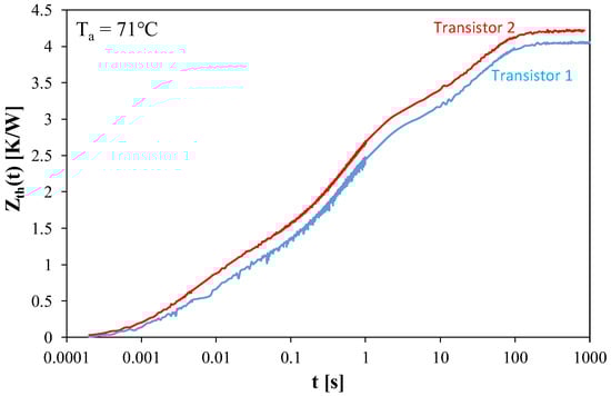
Figure 4.
Transient thermal impedance waveform of samples.
As can be seen, the steady state in the presented Zth(t) waveforms occurs approximately 100 s after the start of cooling (t = 0). The steady-state value of the measured parameter (Rth) ranges from 4 to 4.2 K/W. Comparing this to the manufacturer’s [30] junction-case thermal resistance values, it can be concluded that the remaining components of the heat removal system (MCPCB, heat exchanger, etc.) are responsible for at least 2.4–2.6 K/W of the total thermal resistance of the transistor. The presented Zth(t) waveforms clearly show the segments responsible for heat flow through the individual components of the heat flow path. These components are: the semiconductor chip, the transistor case, the printed circuit board, the thermal interface between the board and the heat exchanger, the heat exchanger, and the cooling fluid.
Using the algorithm described in [18], the values of thermal parameters appearing in Formula (3) were determined for each of the tested transistors. Based on these values, the spectrum of thermal time constants was determined for the measured Zth(t) waveforms shown in Figure 4. The obtained spectra are shown in Figure 5. In this figure, the spectral lines for the Transistor 2 are marked in red, and for the Transistor 1 in blue.
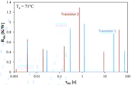
Figure 5.
Spectra of thermal time constants of the considered transistors.
The presented spectrum contains as many as 7 thermal time constants τthi with values ranging from 1 ms to several dozen seconds. The values of τthi for both transistors differ slightly, but these differences are almost imperceptible in the case of the shortest τthi characterizing the thermal properties of the transistor chip and case. The dominant importance is the τthi with a value close to 1 s, which is related to the heat flow between the thermal interface and the heat exchanger. The longest thermal time constants describe thermal properties of the heat exchanger.
Using the determined values of thermal resistance, coefficients ai and thermal time constants τthi, a circuit analog of the thermal model of the tested transistors was formulated in the form of an RC Cauer network [18,19]. This model was implemented in SPICE in the form of the circuit shown in Figure 6 and used to determine the time courses of the junction temperature of the tested transistors by stimulating it from a current source reproducing the measured course of the power dissipated in this transistor.
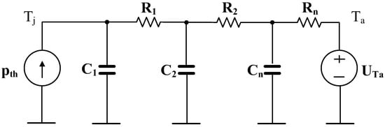
Figure 6.
Thermal model of a tested sample in a form of Cauer network.
Using the thermal model shown in Figure 6, the waveforms of temperature of the most important heat flow path elements were determined when the tested transistor was excited with a rectangular pulses train with a minimum value of 0 and selected maximum values pmax. The computations were performed at a fixed coolant temperature of Ta = 70 °C.
Figure 7 shows the waveforms of the temperature Tj in the steady state obtained for 4 frequency values with a rectangular power waveform of pmax = 30 W.
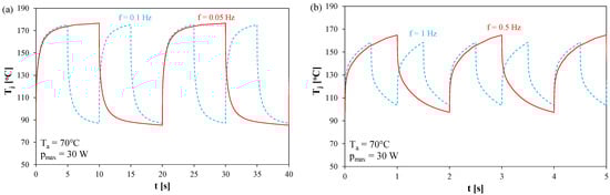
Figure 7.
Computed junction temperature waveforms of the tested transistors operating at frequency values of: (a) 0.05 Hz and 0.1 Hz, (b) 0.5 Hz and 1 Hz.
As can be observed, the peak-to-peak junction temperature increases as the frequency decreases. However, under none of the operating conditions considered does the Tj temperature reach the value corresponding to the transistor being excited by a power step of pmax. This value is the sum of the ambient temperature and the product of the thermal resistance by pmax. Under the conditions considered, this steady-state temperature value would reach 196 °C. It is worth noting that at lower frequency values, a quasi-steady state is observed in every period. At higher frequency values, such a portion of the Tj(t) waveform is not visible. For each of the considered frequency values, the same average Tj temperature value of 133 °C is obtained.
The higher the frequency, the fewer the number of heat transfer components where these stresses are significant. Operating the transistor at too high a frequency can skew the test results, as the potentially most mechanically sensitive component of the heat transfer path will not be subject to significant mechanical stress. This frequency should be selected so that the temperature amplitude is noticeable for all components of the heat transfer path except the cooling system. In the case of the surface-mount power transistors considered in this study, the key element of the heat transfer path is the solder joint between the transistor case and the MCPCB substrate. Its cracking due to temperature changes can lead to deterioration of its metallurgical properties and, consequently, an increase in thermal resistance [33].
Figure 8 shows the results of calculations illustrating the influence of the power waveform period and the transistor thermal model parameters on the peak-to-peak value of the junction temperature waveform ΔTj. To obtain these relationships, transient analyses were performed until a steady state was achieved for the system representing the thermal model (shown in Figure 6) for power in the shape of a rectangular pulse train with a duty cycle of 0.5. The power waveform assumes zero values in the low state and pmax value in the high state. Calculations should be performed for different values of the period. From each of the analyses, the steady-state peak-to-peak junction temperature value is obtained. From each of these analyses, the coordinates of one point in Figure 8 are obtained. The computations were performed for the power pmax = 30 W using the thermal parameters measured for transistors marked as Transistor 1 and Transistor 2.
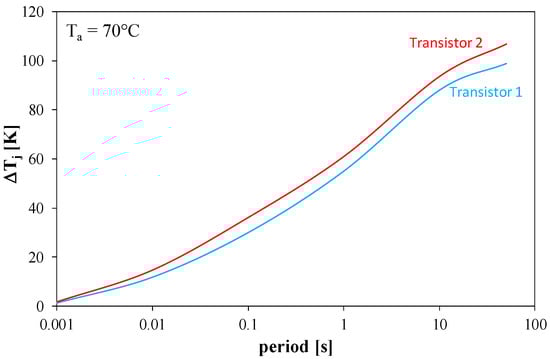
Figure 8.
Dependence of the peak-to-peak value of the transistor junction temperature on the period of the power waveform.
As can be seen, the period of the power waveform strongly affects the value of ΔTj. An increase in the period value from 10 ms to 50 s results in an even seven-fold increase in the value of ΔTj. The curve corresponding to the Transistor 2 transistor lies higher than the curve corresponding to the Transistor 1 transistor, because the values of the thermal time constants for the Transistor 2 transistor are lower. It is worth emphasizing that for all values of the period, an identical average value of the Tj temperature was obtained. The obtained nature of the relationship presented in Figure 8 indicates that operation at higher frequency values (smaller period values) should result in less exposure of the considered transistor to damage due to smaller fluctuations in its junction temperature.
Dependences illustrating the influence of the period on the peak-to-peak value of the junction temperature can be determined for different values of the ambient temperature Ta and for different values of the power amplitude. Of course, for a fixed period value, an increase in the power pmax value results in a higher peak-to-peak temperature value, which can be quickly estimated as the product of this value read from Figure 8 and the quotient of the power pmax by 30 W.
To assess the sensitivity of the tested transistor to power cycling, it is important to determine the peak-to-peak temperature changes of key components in the heat flow path. Figure 9 illustrates the dependence of the steady-state peak-to-peak temperature of components such as the chip, case, and heat exchanger on the period of the power waveform. The amplitude of this waveform is 30 W, and the temperature Ta = 70 °C.
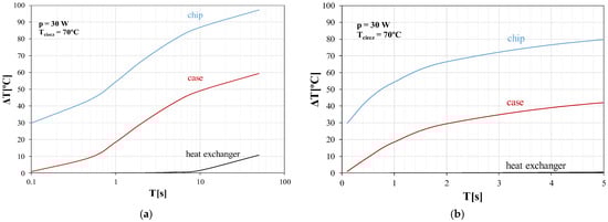
Figure 9.
The computed dependence of the temperature in key points of samples: (a) logarithmic time axis, (b) linear time axis.
As it is result from Figure 9, extending the period of the control signal cause increase in temperature in all points of heat flow path. However, the slope of the considered dependence changes with a change in the period value. For example, an increase in the period from 0.1 s to 1 s results in increase in the chip peak-to-peak temperature value by 25 °C, while an increase in the period from 1 s to 2 s causes only 10 °C increase in the peak-to-peak value of this temperature. Similar changes are observed for the case temperature. It can be seen that the peak-to-peak temperature increases with decreasing frequency.
Based on the presented calculation results, it can be concluded that with the same number of cycles, the probability of damaging the transistor operating at a lower frequency is higher.
3.2. Measurements of Power Cycles
Using the measurement set-up shown in Figure 2, a power cycling test was performed for all transistors selected for testing. The tests were conducted until the tested transistors failed, taking into account the varying frequency of the power dissipation waveform in each tested transistor. During the tests, the waveform of the power dissipation in each transistor was recorded.
For example, Figure 10 shows the measured waveforms of power dissipated in the tested transistors operating at different frequencies from the start of the test until their failure. Figure 10a concerns the transistor operating at a frequency of 0.05 Hz, and Figure 10b, at a frequency of 0.1 Hz.
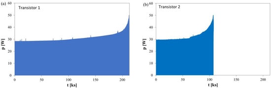
Figure 10.
Measured waveforms of power dissipated in the tested transistors operating at a frequency of: (a) 0.05 Hz, (b) 0.1 Hz.
As can be seen, increasing the frequency shortened the lifespan of the tested transistors. Both measured p(t) waveforms show that for approximately 50% of the test duration, the maximum power value remains almost constant at approximately 28 W, but later on, it increases exponentially. This increase is likely due to degradation of the tested transistor’s properties, manifested, among other things, by an increase in the drain-source on-state resistance. This resistance is an increasing function of the transistor’s junction temperature, which indicates the occurrence of positive feedback, leading to an increase in the RDS(on) resistance, power p, and junction temperature Tj with each operating cycle. The end result is damage to the tested transistors.
To illustrate the effect of frequency and maximum power dissipation in a transistor on its junction temperature, appropriate calculations were performed using SPICE software using a formulated thermal model of the tested transistors. The calculations were performed for two maximum power dissipation values of 28 W and 40 W, respectively. The power was assumed to be a rectangular pulses train with a duty cycle of 0.5, and its value in the off-state was 0.
Figure 11 shows the calculated Tj(t) waveforms for the transistor designated as TRANSISTOR 2 in the thermally steady state. The solid lines refer to the case of power dissipation in this transistor with a maximum value pmax of 30 W, and the dashed lines refer to the value pmax = 40 W. The results shown in Figure 11a were obtained for a frequency of 50 mHz, and in Figure 11b, for a frequency of 0.2 Hz.
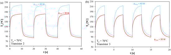
Figure 11.
Computed internal temperature curves of the tested transistors operating at a frequency of: (a) 50 mHz, (b) 0.2 Hz.
As can be seen, at low power waveform frequencies, a very high peak-to-peak temperature is observed within the transistor. For a frequency of 50 mHz, it reaches 85 °C at pmax = 30 W and 130 °C at pmax = 40 W. Increasing the frequency to 0.2 Hz reduces these values to 80 and 120 °C, respectively. It is also worth noting that at peak power pmax = 30 W, the maximum instantaneous temperature Tj slightly exceeds 170 °C, which is close to the maximum permissible operating temperature of the tested transistor. Increasing pmax to 40 W causes the transistor to operate above the maximum permissible temperature, accelerating the damage process. Comparing Figure 11a,b, it can be seen that the average value of the transistor junction temperature for a fixed pmax value does not depend on the frequency and is 130 °C at pmax = 30 W and 150 °C at pmax = 40 W. In turn, a very high peak-to-peak value of the junction temperature causes mechanical stresses to accumulate in the individual components of the transistor and its cooling system during subsequent thermal cycles, causing its damage.
Using the measurement setup shown in Figure 2, power cycling tests were performed for the transistors described in Section 2 at selected supply period values. The first value of the period is equal to the dominant thermal time constant. Each test was continued until the tested transistor, placed on a heat exchanger, was damaged. During the test, the transistor’s VDS voltage waveforms were recorded using an oscilloscope.
When a transistor is damaged, the ID current ceases, and the VDS voltage reaches zero. Once damage is detected, the recorded VDS voltage waveform is analyzed. Based on this waveform, the transistor’s time to failure tlife is read. The quotient of this time and the supply signal period equals the number of cycles to failure Nf. After completing the test for one transistor, it is replaced by another in the measurement system, a new switching frequency is selected, and described above steps are repeated. The test procedure is illustrated in Figure 12.
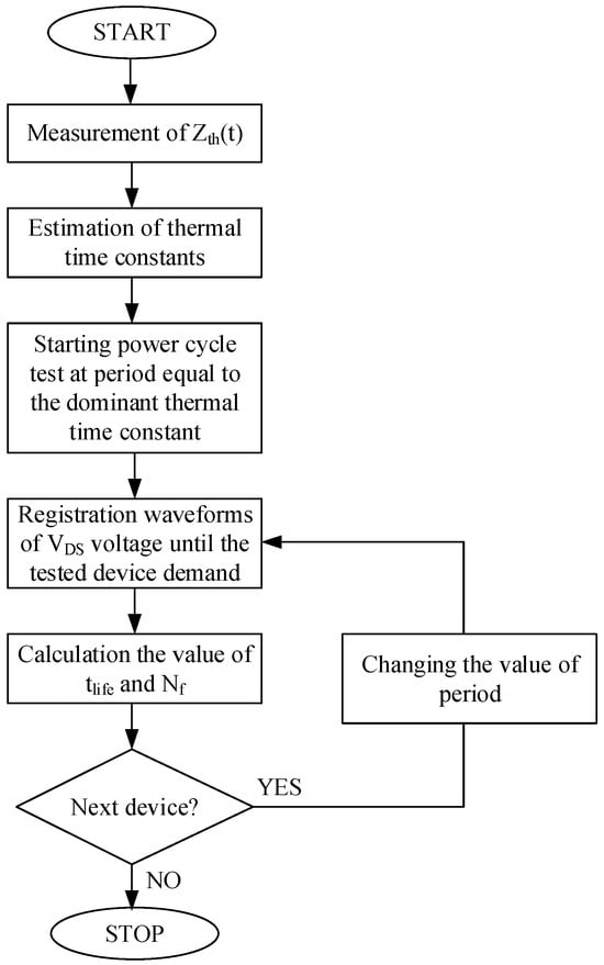
Figure 12.
Flowchart illustrating the manner of performing the tests.
Table 1 presents the results of experimental tests illustrating the dependence of reliability parameters, i.e., lifetime tlife, number of thermal cycles to failure Nf for the tested transistors operating in the circuit shown in Figure 2 at different frequency values. The presented values of tlife and Nf were obtained after the tests performed according to the flowchart shown in Figure 12.

Table 1.
Values of reliability parameters for selected frequency values.
The results in Table 1 indicate that the allowable number of power cycles is almost constant. However, it means that for the considered case increasing amplitude of temperature do not visibly affect number of the cycles obtained in the test, while it highly extend the duration of the test. It is worth to notice, that for the lowest of the considered frequency values, the chip temperature was above the maximum permissible value declared by the manufacturer for almost half of each period. For the period equal to 5 s (f = 200 mHz), the obtained number of Nf was significantly different than for other considered cases. Following the authors experience it is related to repeatability of the samples.
4. Influence of Activation Energy on Lifetime
The results presented in Section 3 concern the operation of the tested transistors at elevated ambient temperatures. According to the classical Arrhenius formula [3], the device lifetime until failure τ at temperature Tj can be described by the relationship (1). By determining the quotient τ/τ0 from this relationship, hereinafter referred to as the acceleration factor, it is possible to estimate how many times greater the value of the time tlife at room temperature will be than the value given in Table 1. For this purpose, it is necessary to determine the activation energy Ea of the failure processes occurring in the tested transistor.
The activation energy varies for different physical and chemical damage mechanisms. Therefore, when calculating acceleration coefficients to determine the damage activation energy, it is necessary to determine the mechanisms causing the damage. Paper [8] states that the activation energy for assembly-related damage ranges from 0.5 to 0.7 eV. Activation energy values of approximately 1 eV are found for many important degradation mechanisms in semiconductor materials. These include phenomena such as diffusion, migration of atoms within the semiconductor material, chemical reactions that can change the material’s composition, and ion migration under the influence of an electric field.
In order to illustrate the influence of the activation energy value on the lifetime of the components, the dependencies τ/τ0(Tj) were determined for selected Ea values equal to 0.3 eV, 0.5 eV, 0.7 eV and 1 eV, respectively. These dependencies are shown in Figure 13. In this figure, the scale in the vertical axis is logarithmic.
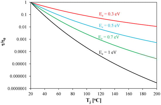
Figure 13.
Relative change in transistor lifetime as a function of temperature.
From Figure 13, it can be seen that an increase in temperature shortens the lifetime and reduces the expansion factor. At the lowest activation energy value considered, a temperature increase of 100 °C (from 20 to 120 °C) results in a reduction in this factor only 20 times. In turn, at Ea = 1 eV, the same temperature increase results in a reduction in the expansion factor by as much as over 20,000 times.
Table 2 shows the effect of a temperature change from 70 °C to 20 °C on the acceleration coefficient value at selected values of activation energy Ea.
Table 2.
Acceleration coefficient values when the temperature changes from 70 °C to 20 °C at selected activation energy values calculated using Equation (1).
As can be seen, increasing the activation energy causes an exponential increase in the acceleration factor. For the considered range of Ea changes, the acceleration factor increases by a factor of 100. Assuming a typical activation energy value of Ea = 0.75 eV, a temperature change from 70 °C to 20 °C results in a lifetime extension of over 75 times.
Taking into account the above considerations and the data from Table 1, the lifetime of the tested transistors can be estimated at any coolant temperature. Assuming an activation energy of 0.75 eV for the failure process and the measured number of cycles to failure, it can be concluded that the lifetime under the transistor power supply conditions established during the test is a decreasing function of frequency.
Combining information presented in Table 1 and Table 2, the values of lifetime of the tested transistors corresponding to a temperature equal to 20 °C were calculated for all the considered frequency values. For example, at a temperature of 20 °C, the lifetime decreases from approximately 4500 h at f = 50 mHz to 400 h at f = 0.5 Hz. Of course, this lifetime will increase as the value of pmax decreases. For example, at a power of pmax = 14 W, the average temperature value Tj will decrease to 100 °C. At the considered value of Ea = 0.75 eV, using Equation (1), it is easy to observe that such a decrease in Tj will mean an approximately 8-fold increase in lifetime. At the abovementioned value of frequency f = 0.05 Hz, the lifetime will therefore be 32,000 h.
5. Conclusions
This paper presents the results of experimental and simulation studies illustrating the effect of a transistor’s operating frequency on the number of thermal cycles it can endure without failure and its lifetime. Studies conducted at elevated ambient temperatures indicate that for low switching frequencies, there is almost no difference in the allowable number of thermal cycles as the frequency changes in the millihertz range. Therefore, the lifetime is longest at the lowest frequency considered.
Analysis of the time-varying power dissipation patterns in the tested transistors indicates that the damage process is initiated by self-heating. This causes an increase in the junction temperature, which in turn increases the drain-source on-state resistance. This translates into an increase in the average power dissipated in the transistor and an increase in its junction temperature (both the average and peak-to-peak values). A positive feedback loop therefore occurs, ultimately causing the junction temperature of the transistor to significantly exceed the permissible value and ultimately causing damage. In the tested transistors, it was observed that immediately before the damage, the power dissipated in the transistor during its on-state was almost twice as high as at the beginning of the test.
Computer simulations were also conducted to illustrate the temporal changes in the transistor’s junction temperature during the tested thermal cycles. It was found that as the transistor’s switching frequency decreases, an increase in the peak-to-peak temperature Tj is observed. Under the conditions considered in these studies, this value can exceed 70 °C.
Based on the literature data, analyses were conducted to determine the effect of the activation energy of the damage process and the ambient temperature on the shortened lifespan. Based on the results of these analyses, the room temperature lifetimes of the tested transistors were estimated. It was shown that operating the considered transistor within a switching period close to the dominant thermal time constant results in accelerated damage processes. The value of this thermal time constant in the considered cooling system is approximately 1 s, while in typical systems using natural convection cooling, this time constant can range from several dozen to several thousand seconds [17,18,20]. In such a case, achieving a high peak-to-peak temperature Tj will require a significantly lower switching frequency.
The research carried out shows that it is important to pay particular attention to selecting the period for the active thermal cycling test. Selecting it based on thermal time constants may significantly shorten the duration of the test without affecting the obtained results, even though the amplitude of the chip temperature significantly decreased.
In light of the measurement standards, it is important to consider this issue, since the period of the control signal is not precisely defined. The maximum period specified in well-known standards is fitted for large power modules, not surface-mounted discrete power transistors.
The obtained research results may be useful to designers of power electronic devices, allowing them to properly select the operating conditions of the transistor to guarantee the expected value of its failure-free operation time. In future investigations, we will try to elaborate on any formula describing the influence of thermal cycle frequency on the lifetime. This task requires many time-consuming tests to be performed at different frequency values.
Author Contributions
Conceptualization: K.G. and P.G.; methodology: P.G.; investigation: P.G.; writing—original draft preparation: K.G. and P.G.; writing—review and editing: K.G. and P.G.; visualization: K.G. and P.G.; supervision: K.G. All authors have read and agreed to the published version of the manuscript.
Funding
This research received no external funding.
Data Availability Statement
The original contributions presented in this study are included in the article. Further inquiries can be directed to the corresponding author.
Conflicts of Interest
The authors declare no conflicts of interest.
References
- Bąba, S.; Gieraltowski, A.; Jasiński, M.; Blaabjerg, F.; Bahman, A.S.; Zelechowski, M. Active Power Cycling Test Bench for SiC Power MOSFETs—Principles, Design, and Implementation. IEEE Trans. Power Electron. 2021, 36, 2661–2675. [Google Scholar] [CrossRef]
- Peyghami, S.; Blaabjerg, F.; Palensky, P. Incorporating Power Electronic Converters Reliability into Modern Power System Reliability Analysis. IEEE J. Emerg. Sel. Top. Power Electron. 2021, 9, 1668–1681. [Google Scholar] [CrossRef]
- Gładysz, H.; Brzuszkiewicz, T.; Żukowski, A. Niezawodność Przyrządów Półprzewodnikowych; Wydawnictwo Przemysłowe WEMA: Warszawa, Poland, 1989. [Google Scholar]
- Górecki, K.; Kowalke, W.; Ptak, P. Influence of Quality of Mounting Process of RF Transistors on Their Thermal Parameters and Lifetime. Appl. Sci. 2022, 12, 6113. [Google Scholar] [CrossRef]
- Gopalakrishna, H.; Sinha, A.; Carpenter, J.; Niverty, S. Activation Energy for End-of-Life Solder Bond Degradation: Thermal Cycling of Field-Aged PV Modules. IEEE J. Photovolta. 2020, 10, 1762–1771. [Google Scholar] [CrossRef]
- Alam, M.S.; Basit, M.; Suhling, J.C.; Lall, P. Mechanical Characterization of SAC305 Lead Free Solder at High Temperatures. In Proceedings of the 2016 15th IEEE Intersociety Conference on Thermal and Thermomechanical Phenomena in Electronic Systems (ITherm), Las Vegas, NV, USA, 31 May–3 June 2016; pp. 755–760. [Google Scholar] [CrossRef]
- Liu, Y.; Chuong, K.; Zhang, Z.J.; Garten, L.M.; Graber, L. Failure modes and remedies of a solid-state low voltage DC circuit breaker through 3,000,000+ operation cycles. Power Electron. Devices Compon. 2025, 12, 100119. [Google Scholar] [CrossRef]
- Zhao, S.; Yang, X.; Wu, X.; Liu, G. Investigation on Creep-Fatigue Interaction Failure of Die-Attach Solder Layers in IGBTs Under Power Cycling. IEEE Trans. Power Electron. 2025, 40, 7261–7274. [Google Scholar] [CrossRef]
- Morel, C.; Morel, J.-Y. Power Semiconductor Junction Temperature and Lifetime Estimations: A Review. Energies 2024, 17, 4589. [Google Scholar] [CrossRef]
- Wu, X.; Yang, X.; Ye, J.; Liu, G. Novel Prognostics for IGBTs Using Wire-Bond Contact Degradation Model Considering On-Chip Temperature Distribution. IEEE Trans. Power Electron. 2025, 40, 4411–4424. [Google Scholar] [CrossRef]
- Wen, Q.; Zhai, R.; Ji, G.; Zhu, T.; Li, Z.; Hue, Y. Test Method and Application of High-Temperature Operating Life of Automobile Chips. J. Phys. Conf. Ser. 2023, 2447, 012003. [Google Scholar] [CrossRef]
- Ericson, R.; Maksimovic, D. Fundamentals of Power Electronics; Springer Nature Switzerland AG: Cham, Switzerland, 2020. [Google Scholar]
- Zhang, L.; Yuan, X.; Wu, X.; Shi, C.; Zhang, J.; Zhang, Y. Performance Evaluation of High-Power SiC MOSFET Modules in Comparison to Si IGBT Modules. IEEE Trans. Power Electron. 2019, 34, 1181–1196. [Google Scholar] [CrossRef]
- Winkler, R. Thermal Properties of High-Power Transistors. IEEE Trans. Electron Devices 1967, 14, 260–263. [Google Scholar] [CrossRef]
- Stala, R.; Piłat, A.; Chojowski, M.; Skowron, M.; Folmer, S. Thermal and Electric Parameter Analysis of DC–DC Module Based on Resonant Switched Capacitor Converter. Energies 2022, 15, 7040. [Google Scholar] [CrossRef]
- Herold, C.; Franke, J.; Bhojani, R.; Schleicher, A.; Lutz, J. Requirements in power cycling for precise lifetime estimation. Microelectron. Reliab. 2016, 58, 82–89. [Google Scholar] [CrossRef]
- Górecki, K.; Górecki, P. SPICE-aided nonlinear electrothermal modeling of an IGBT module. Electronics 2023, 12, 4588. [Google Scholar] [CrossRef]
- Górecki, K.; Zarębski, J.; Górecki, P.; Ptak, P. Compact thermal models of semiconductor devices—A review. Int. J. Electron. Telecommun. 2019, 65, 151–158. [Google Scholar] [CrossRef]
- Janicki, M.; Sarkany, Z.; Napieralski, A. Impact of nonlinearities on electronic device transient thermal responses. Microelectron. J. 2014, 45, 1721–1725. [Google Scholar] [CrossRef]
- Górecki, K.; Ptak, P.; Janicki, M. Investigations of mutual thermal couplings in selected lighting sources with power LEDs. IEEE Trans. Compon. Packag. Manuf. Technol. 2023, 13, 1130–1138. [Google Scholar] [CrossRef]
- Castellazzi, A.; Kraus, R.; Seliger, N.; Schmitt-Landsiedel, D. Reliability analysis of power MOSFET’s with the help of compact models and circuit simulation. Microelectron. Reliab. 2002, 42, 1605–1610. [Google Scholar] [CrossRef]
- Ciappa, M.; Carbognami, F.; Cora, P.; Fichtner, W. A novel thermomechanics-based lifetime prediction model for cycle fatigue failure mechanisms in power semiconductors. Microelectron. Reliab. 2002, 42, 1653–1658. [Google Scholar] [CrossRef]
- Szekely, V. A new evaluation method of thermal transient measurement results. Microelectron. J. 1997, 28, 277–292. [Google Scholar] [CrossRef]
- An, T.; Zhou, R.; Qin, F.; Dai, Y.; Gong, Y.; Chen, P. Comparative Study of the Parameter Acquisition Methods for the Cauer Thermal Network Model of an IGBT Module. Electronics 2023, 12, 1650. [Google Scholar] [CrossRef]
- Górecki, K.; Posobkiewicz, K. Selected Problems of Power MOSFETs Thermal Parameters Measurements. Energies 2021, 14, 8353. [Google Scholar] [CrossRef]
- Azoui, T.; Tounsi, P.; Dorkel, J.-M. Innovative methodology to extract dynamic compact thermal models: Application to power devices. Microelectron. J. 2012, 43, 642–648. [Google Scholar] [CrossRef]
- Jakani, A.; Sommet, R.; Simbélie, F.; Nallatamby, J.-C. Understanding the Thermal Time Constants of GaN HEMTs through Model Order Reduction Technique. Electronics 2021, 10, 3138. [Google Scholar] [CrossRef]
- Yang, L.; Hu, J.; Shin, M.W. Dynamic Thermal Analysis of High-Power LEDs at Pulse Conditions. IEEE Electron Device Lett. 2008, 29, 863–866. [Google Scholar] [CrossRef]
- Hegedüs, J.; Hantos, G.; Lukács, M.; Bodnár, B.; Lipák, G.; Poppe, A. Lifetime test of pulse width modulated LEDs supplemented with thermal investigations. IEEE Trans. Compon. Packag. Manuf. Technol. 2023, 13, 1121–1129. [Google Scholar] [CrossRef]
- IPB090N06N3 G, Datasheet, Infineon Technologies. Available online: https://www.infineon.com/dgdl/Infineon-IPP_B093N06N3-DS-v01_02-en.pdf?fileId=db3a30432313ff5e0123a3593b1425eb (accessed on 17 November 2025).
- Avenas, Y.; Dupont, L.; Khatir, Z. Temperature measurement of power semiconductor devices by thermo-sensitive electrical parameters—A review. IEEE Trans. Power Electron. 2012, 27, 3081–3092. [Google Scholar] [CrossRef]
- AC200 Immersion Circulators. Available online: https://www.thermofisher.com/order/catalog/product/156-0001 (accessed on 17 November 2025).
- Schmid, M.; Hermann, J.; Bhogaraju, K.; Elger, G. Reliability of SAC Solders under Low and High Stress Conditions. In Proceedings of the 9th IEEE Electronics System-Integration Technology Conference (ESTC), Sibiu, Romania, 13–16 September 2022; pp. 553–559. [Google Scholar]
Disclaimer/Publisher’s Note: The statements, opinions and data contained in all publications are solely those of the individual author(s) and contributor(s) and not of MDPI and/or the editor(s). MDPI and/or the editor(s) disclaim responsibility for any injury to people or property resulting from any ideas, methods, instructions or products referred to in the content. |
© 2025 by the authors. Licensee MDPI, Basel, Switzerland. This article is an open access article distributed under the terms and conditions of the Creative Commons Attribution (CC BY) license (https://creativecommons.org/licenses/by/4.0/).