Abstract
Traditional symmetric voltage multiplier-based structures offer low current stress and high scalability. However, the equalization current flowing into each energy storage cell must overcome four diode voltage drops per switching cycle, significantly degrading energy transfer efficiency. A compact integrated equalizer based on multi-stacked buck-boost converters for large-scale energy storage systems is proposed. By replacing diodes with inductors, the design achieves high-efficiency cell balancing even at low cell voltages. The integrated design leverages the boost circuit’s inherent current ripple for driving the balancing system, eliminating extra switches and minimizing size and cost. Additionally, it provides independent balancing channels for each cell, eliminating equalization current superposition. This reduces cell current stress while enabling large-scale system balancing. Experimental validation on an eight-cell setup demonstrated successful balancing with 87.5% system efficiency.
1. Introduction
Large-scale battery energy storage systems (LS-BESS) are pivotal for integrating renewable energy and enhancing grid flexibility [1,2]. However, the LS-BESS performance, lifespan, and safety are fundamentally constrained by cell inconsistencies, which arise from manufacturing variations and operational conditions [3]. The presence of voltage imbalances among cells can trigger overcharging or over-discharging, which in turn accelerates cell degradation and introduces significant safety risks [3]. Thus, advanced battery management, particularly efficient equalization techniques, is critical to ensuring the reliability and economic viability of such systems.
Retired lithium batteries (RLB) from electric vehicles offer the advantages of lower cost and higher energy density compared to traditional lead-acid battery packs [4]. RLB is extensively utilized in “low-intensity” usage scenarios such as electric bicycles, 5G base station energy storage systems, and home energy storage systems [5]. However, even with RLBs undergoing capacity sorting or consistency screening, differences persist among individual cells in terms of lifespan, cycle count, charge–discharge current rates, operating temperatures, and internal resistances [6]. Operationally, the “weakest link” phenomenon dictates that the lowest-capacity cell sets the usable limit for the entire battery pack. Capacity variations give rise to a reduction in overall pack performance and can drive individual cells into abusive operational states (overcharging/discharging), thereby causing accelerated degradation and potential safety incidents, including fire. Therefore, the implementation of a battery equalization system is paramount to ensure the safe and stable functioning of RLB [7].
In the passive balancing approach [8], resistors are configured in parallel with cells at higher voltages to divert and dissipate surplus charge, thus establishing system balance. However, the passive balance method can only ensure cell balance and cannot increase battery pack capacity. Additionally, the passive balance method has lower balancing current and system efficiency. Active balance methods include switch-capacitor [9,10,11], switch-inductor [12,13], multi-winding transformer [14,15,16,17,18], switch-matrix [19,20], voltage multiplier [21,22,23], and wireless power transfer [24,25,26]. The active balance method allocates energy to low-voltage cells, achieving system balance with higher efficiency and a larger balancing current.
Utilizing a network of switches and capacitors, the switched-capacitor equalizer operates by transferring energy from higher-voltage cells to their lower-voltage counterparts. A fundamental limitation of this method is that its balancing current exhibits a strong correlation with the voltage disparity among cells, consequently yielding low efficiency during the final stages of balancing when voltages converge [27]. To address the need for higher balancing currents, Ye et al. developed a method capitalizing on LC resonance through switched-resonant capacitors [28]. Building upon this, Shang et al. further improved the energy transfer pathway with a star-structured switched-capacitor equalizer [29]. This topology enables direct, parallel energy transfer from high-voltage to low-voltage cells, significantly boosting the energy transfer rate.
The switch-inductor-based equalizer is proposed to increase balancing currents, which operate on the same principle as a buck-boost converter [30]. The balancing current can be precisely controlled by modulating the duty cycle of the MOSFET. Conversely, conventional switched-inductor equalizers can only shift energy between immediately neighboring batteries. For superior performance in energy transfer, Xu et al. introduced a novel integrated balancing method based on inductive coupling, which facilitates direct energy exchange between adjacent batteries [13]. A key feature of this design is the use of separate buck-boost converters and coupled inductors for each cell, allowing energy to be shuttled efficiently from high-voltage to low-voltage cells and leading to a markedly improved energy transfer rate.
To minimize the switch count in equalization circuits, a balanced structure utilizing multi-winding transformers has been proposed. Larger balancing currents flow through low-voltage cells using secondary windings with the same number of turns to output the same voltage. To address scalability in large battery packs, Shang et al. introduced an innovative balancing architecture using a modularized multi-winding transformer, employing forward converters within modules to balance individual cells and flyback converters between modules to achieve inter-module balancing [14], eliminating residual magnetism within the transformer. Xu et al. leveraged the Zeta circuit to create an integrated balancing structure. This topology utilizes the circuit’s inherent switches to achieve simultaneous balancing between supercapacitors and the battery pack [31]. Integrated multi-winding transformers leverage additional balancing circuits inherent in DC-DC converters, thereby avoiding the addition of extra switches and resulting in a more compact and cost-effective system.
Uno et al. proposed an integrated balancing structure based on voltage multipliers [32], utilizing the voltage multiplier to output the same voltage at each port, thus achieving battery pack balancing. Uno also improved the multi-stacked buck-boost converters and star-structured switched-capacitor equalizers integrated balancing system to realize balancing functionality without additional switches [33]. An integrated, self-modularized design was introduced by Tan et al., which combines a battery equalizer with a supercapacitor charger to enhance the scalability of voltage multipliers in hybrid electric applications. The battery equalization structure and the supercapacitor charging equalizer are integrated into a circuit with only two switches, three inductors, several energy storage capacitors, and diodes. This integration effectively reduces both the size and cost of the system. Uno et al. first proposed the multi-stacked super buck-based equalization structure, which utilizes inductors instead of diodes to achieve battery pack equalization, effectively improving system efficiency [26]. His subsequent work introduced transformer-less, single-switch integrated chargers, achieving system and circuit simplification through the integration of the charger and equalizer into a single unit [34].
However, as the number of series-connected cells in energy storage systems increases, the traditional voltage multipliers balancing circuit causes high current stress on intermediate cells during balancing, as all balancing current flows through them.
In the realm of balancing circuits, recent advancements are predominantly centered on wireless power transfer and their integrated applications. A notable contribution comes from Zhang et al., who employed a multi-winding transformer in a wireless power transfer-based design to balance numerous voltage multipliers, thereby effectively enhancing system scalability [25,26,34]. Further innovations include the switch-based strategy at receiving ports by Cai et al. for anti-misalignment charging [35], and the multi-layer voltage multiplier topology by Liu et al. for improved transfer efficiency [36]. Nevertheless, all these circuits share a fundamental drawback: the inherent use of voltage multipliers results in significant current stress on individual cells.
To mitigate current stress in cells, Yang et al. [23] presented a voltage equalizer that combines a boost full-bridge input cell with a symmetric VM circuit for long battery packs, thereby alleviating stress on the energy storage units. Owing to its symmetric architecture, energy is transferred directly through individual cells, making the system compatible with both battery and supercapacitor applications. A key drawback of this symmetrical VM system is its doubled voltage drop per cycle. The accumulation of more diode forward voltages per cycle directly undermines its efficiency relative to other topologies at the same cell voltage [37]. This inefficiency is particularly pronounced in real-world scenarios, where the inherently low voltage of individual cells is further diminished by the current being subjected to two diode drops every switching cycle [38], compounding the inherent inefficiency.
This work therefore presents a compact, integrated equalizer based on a multi-stacked buck-boost converter for large-scale energy storage systems. In this design, a boost DC-DC circuit efficiently channels energy into the multi-stacked buck-boost converter. Key contributions of this study include the following:
- (1)
- The system requires only one transformer, and the additional balancing system does not necessitate extra switches, effectively reducing system volume.
- (2)
- Employing a symmetric structure ensures that balancing on Bn2 does not pass through Bn1, mitigating issues of uneven current stress that can lead to premature aging in hierarchical battery packs compared to existing structures.
- (3)
- The proposed equalizer improves the overall energy transfer efficiency of the system by replacing diodes with inductors.
2. Operation Analysis
In the voltage equalizer structure combining a boost full-bridge inverter with a symmetrical voltage multiplier, the balancing current must pass through four diodes during a single operating cycle. This path entails a substantial diode voltage drop, which consequently diminishes the system’s energy transfer efficiency. The schematic diagram of the traditional voltage equalizer based on a boost full-bridge inverter and symmetrical voltage multiplier is presented in Figure 1. To overcome these limitations, a compact integrated equalizer based on a multi-stacked buck-boost converter is proposed for large-scale energy storage systems, as illustrated in Figure 2. By replacing diodes with inductors, the energy transfer efficiency can be effectively improved during the energy transmission process.
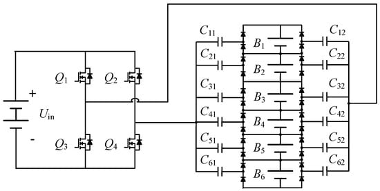
Figure 1.
The structure of the voltage equalizer based on boost full-bridge inverter and symmetrical voltage multiplier.
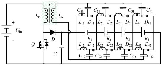
Figure 2.
The structure of the symmetric multi-boost-buck based equalizer, and the green part is the drive transformer.
Figure 1 shows the circuit topology of the conventional symmetric VM designed for long battery packs. The DC power supply uses an inverter to power the symmetric VM balance structure, driving the symmetric VM with alternating current. The symmetrical VM is mainly composed of diodes Dn1–Dn4 and transfer capacitors Cn1 and Cn2. The working process of the VM can be categorized into two distinct modes.
Mode I (t0 − t1) iC1_I flows into UC1 through the transmission capacitors C11 and C12 and diodes D11 and D14. iC2_I flow into UC2 through the transmission capacitors C21 and C22 and diodes D21 and D24, as shown in Figure 3.
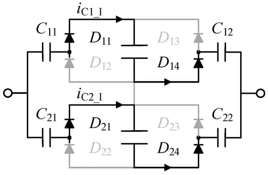
Figure 3.
The working process of the symmetric VM in mode I.
Mode II (t1 − t2) iC1_II flows into UC2 through the transmission capacitors C11 and C12 and diodes D12 and D13. iC2_II flows into UC2 through the transmission capacitors C21 and C22 and diodes D22 and D23, as shown in Figure 4.
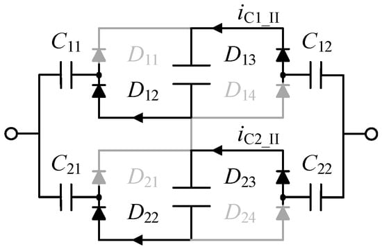
Figure 4.
The working process of the symmetric VM in mode II.
Figure 3 and Figure 4 demonstrate that the current path flows through two diodes, thereby ensuring a consistent path length under both positive and negative input voltages. Given a diode forward voltage drop of 0.53 V and a cell voltage of 2.5 V, the power loss solely from the diode accounts for nearly 29.7% in one cycle. When a cell voltage is 3.65 V, the power loss solely from the diode accounts for nearly 22.5% in one cycle, resulting in low energy transfer efficiency for the system.
To improve the equalization efficiency of symmetric VM at low voltage, a multi-Boost-Buck based equalizer is proposed. To avoid double voltage drops in one cycle, a diode is replaced by one inductor in the proposed structure. The working process of the VM is categorized into two distinct modes, presented in Figure 5 and Figure 6.
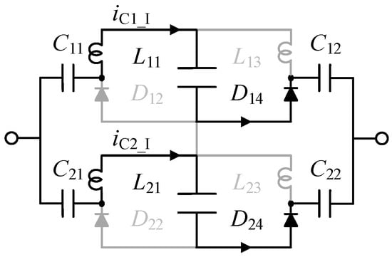
Figure 5.
The working process of the symmetric multi-boost-buck based equalizer in mode I.
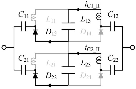
Figure 6.
The working process of the symmetric multi-boost-buck based equalizer in mode II.
Therefore, the amount of electricity flowing into the capacitor Cn1 is equal to the amount of electricity flowing out during each cycle.
As shown in Figure 5 and Figure 6, energy flow passes through one diode regardless of whether the input voltage is positive or negative. Given a diode forward voltage drop of 0.53 V and a cell voltage of 2.5 V, the power loss solely from the diode accounts for nearly 17.5% in one cycle. When a cell voltage of 3.65 V, the power loss solely from the diode accounts for nearly 12.6% in one cycle.
Compared to the traditional symmetric VM equalizer, the proposed topology effectively mitigates the detrimental impact of diode voltage drops on system efficiency. Therefore, the proposed equalizer achieves a 10–12% gain in balancing efficiency within large-scale energy storage systems. While inductors were not considered in this simplified analysis, their nature as energy storage components means that, their parameters can be optimized to further enhance system performance.
Design of the Proposed Integrated Equalizer
A scalable, multi-stacked buck-boost topology is introduced for voltage equalization in energy storage systems, as illustrated in Figure 7. The core balancing mechanism employs a symmetrical buck-boost converter design, where the equalizing current is confined to flow solely through its respective cell. The circuit incorporates transfer capacitors (C11–Cnm), a transformer secondary winding (LS), transfer inductors (L11–Lnm), and diodes (D11–Dnm). Battery units B1 through B4, with respective voltages UB1–UB4, are connected to the system. Additionally, a boost converter is formed by switch Q, diode D, the main inductor Lm, and capacitor C.
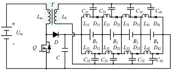
Figure 7.
The structure of the proposed equalizer, and the green part is the drive transformer.
Mode I [t0 − t1, Figure 8]: As depicted in Figure 8, when switch Q is turned on, the boost converter is activated, energizing inductor Lm. A voltage is then induced in the secondary winding LS, driving a current (in_I) that flows through batteries B1 to B4. This current loop is completed back to inductor Lm via components Cn2, Ln1, Dn2, and Cn1. Simultaneously, the current iLn_I through inductor Ln2 continues to conduct via battery Bn and diode Dn2.
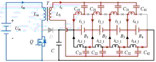
Figure 8.
Operating phases of the proposed equalizer at Mode I. The blue part is the battery charging circuit, and the red part is the balancing circuit.
The equation for the freewheeling current in_I is as follows:
where ILn_I is the initial current of the Ln2.
Mode II [t1 − t2, Figure 9]: As depicted in Figure 9, when switch S remains on, the current iLn_I becomes 0. The boost converter is activated, energizing inductor Lm. This current (in_I) is completed back to inductor Lm via components Cn2, Ln1, Dn2, and Cn1.
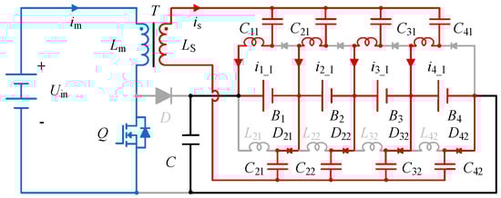
Figure 9.
Operating phases of the proposed equalizer at Mode II. The blue part is the battery charging circuit, and the red part is the balancing circuit.
When the power source energizes the inductor Lm, the charging current im increases. This current drives the transformer, and the voltage at the multi-winding ports is given by the following:
where N is the winding turns ratio of the transformer.
The voltage of the VLm satisfies the following:
where rn is the equivalent resistance of the balance circuit loop, and VDnm is the voltage drop of the Dnm. VCn1 and VCn2 represent the voltages across capacitors Cn1 and Cn2, respectively.
Balancing current iLn_I is given by the following:
Balance current ILn_I is given by the following:
Mode III [t2 − t3, Figure 10]: When switch Q is turned off, the boost converter enters the discharging phase, where the combined energy from the DC source and inductor Lm is delivered to charge the battery pack. During this period, a current ripple is observed in inductor Lm. Simultaneously, a reverse voltage is induced in the secondary winding LS, generating a current i1_II. This current flows out to charge the series-connected batteries B1 through B4 and subsequently passes through components Cn2, Ln2, Bn, and Dn1, before returning to inductor LS via Cn1. Meanwhile, inductor Ln1 maintains its current circulation through Bn and Dn1.
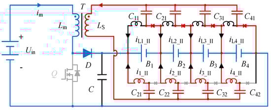
Figure 10.
Operating phases of the proposed equalizer at Mode III. The blue part is the battery charging circuit, and the red part is the balancing circuit.
Therefore, the continuous current equation for in_II.
where In_I is the initial current of the Ln1. Therefore, upon completion of this phase, the current in_I will drop to zero.
Mode IV [t3 − t4, Figure 11]: When switch Q remains off, this current flows out to charge the series-connected batteries B1 through B4 and subsequently passes through components Cn2, Ln2, Bn, and Dn1, before returning to inductor LS via Cn1.
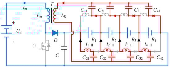
Figure 11.
Operating phases of the proposed equalizer at Mode IV. The blue part is the battery charging circuit, and the red part is the balancing circuit.
During the charging of inductor Lm by the power source, the rising magnetizing current im drives the transformer. The voltage it establishes across the multi-winding ports can be defined by the following:
The voltage of the VLnm is given by the following expression:
Balancing current inm is given by the following:
Balance current In_II is given by the following:
From (10), the current flowing into the battery over one cycle can be expressed as follows. The higher the actual voltage VBn, the greater the balancing current In_I and In_II. When VBn is smaller, the balance current is larger. Thus, the system enables battery charge balancing.
For the proposed topology, the reference directions for all currents and voltages are defined as follows (Figure 12):
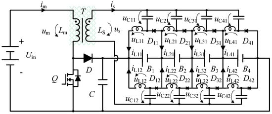
Figure 12.
Reference directions of currents and voltages in the proposed topology, and the green part is the drive transformer.
For the loop formed by Ls,Ci1, Li1, Li2, and Ci2, the Kirchhoff’s voltage equation is given by:
where uLi1 represents the voltage across inductor Li1, uLi2 denotes the voltage across inductor Li2, UCi1 is the average voltage across capacitor Ci1, and UCi2 is the average voltage across capacitor Ci2. According to the volt-second balance principle, the average value of the inductor voltage over one switching period must be zero under steady-state conditions to ensure proper core reset of the magnetic components. Therefore, the averaged form of Equation (11) is derived as follows:
Substituting the above expression into Equation (11) yields the following:
For Mode 1, the current flow direction in the circuit is illustrated in Figure 9 below when the circuit operates in DCM.
For the charging loop formed by Ls, Ci1, Li1, Bi, Di2, Ci2, the corresponding Kirchhoff’s voltage equation can be written as follows:
Substituting the above into Equation (14) gives the following:
Since the MOSFET is turned on at this stage, it follows that:
Substituting this equation back into Equation (15) results in the following:
Assuming the converter duty cycle is D, the final values of the inductor currents iLm.I, iLi1.I, and iLi2.I at the end of Mode 1 are given by the following:
If the turn-off time of the MOSFET prior to Mode 1 is sufficiently long, diodes Di1 and Di2 are both off before Mode 1 begins. Thus, in discontinuous conduction mode (DCM), the currents iLm.DCM, iLi1.DCM and iLi2.DCM are zero.
For Mode 2, the current flow direction in the circuit is shown in Figure 10.
Applying the same method, the KVL equation for the charging loop formed by Ls, Ci1, Li2, Bi, Di1, Ci2, can be written as follows:
This leads to the following:
At this stage, since the MOSFET is turned off the following:
Substituting into Equation (20) gives the following:
Meanwhile, the voltage across inductor Li1 satisfies the following:
Therefore, the final current values at the end of this mode can be given by the following:
where Da1 is the ratio of the time required for the current in inductor Li1 to decrease from iLi1.I to zero to the switching period in DCM, and Da2 is the corresponding ratio for the primary winding inductor current decreasing from iLm.I to zero. Setting iLi1.II and iLm.II to zero and combining Equations (18) and (24), we obtain the following:
After the inductor current iLi2.II in DCM 2 drops to zero, inductor Li2 freewheels through the battery and diode, resulting in the following:
Setting the final current iLi2.III to zero gives the following:
When the current in inductor Li2 decreases to zero, the current in the loop becomes discontinuous, and iLm.DCM, iLi1.DCM and iLi2.DCM are all zero.
Thus, the average currents of the respective inductors can be solved as follows:
From this, the following can be derived:
where K is given by:
Based on the average current levels of inductors Lm, Li1, and Li2, the required inductor parameters can be calculated.
The duty cycle is controlled to regulate both the input and charging voltages. The resulting relationship between the input and output voltage is derived as follows:
where D is the duty cycle.
A feedback control loop, utilizing the battery current (IB) and voltage (VB) as inputs, adjusts the duty cycle D of switch Q (see Figure 13). This mechanism guarantees that the boost circuit operates in constant-current or constant-voltage charging modes as required.
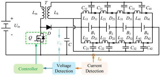
Figure 13.
Control block of the proposed method.
3. Implementation and Experimental Results
To demonstrate the proposed voltage equalizer, an experimental platform was built with eight WTGR7V55F00Z ultracapacitor cells (5 F, 0–7.5 V operating range per cell), as shown in Figure 14. The transformer utilizes an iron oxide toroidal core. The key parameters of the proposed design are listed in Table 1.
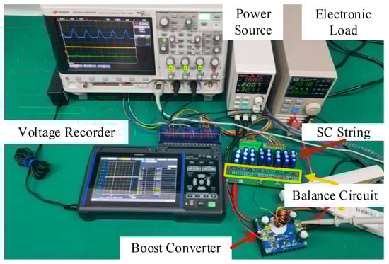
Figure 14.
Photograph of the experimental prototype for the eight-series UC modularized equalizer.

Table 1.
Specifications of the multi-stacked buck-boost based equalizer.
Figure 15 shows the balance current iLS in the secondary coil LS of the balancing transformer. The boost output voltage uB, and the boost output current iB.
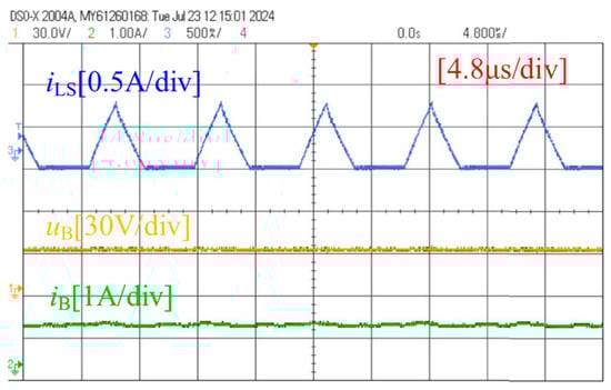
Figure 15.
The experimental waveforms currents iL, VB, and iB.
The inherent low capacity of the UC cell rules out single-cycle balancing. Therefore, verification was conducted by paralleling an electronic load (set to constant voltage mode) with the UC string and performing a series of tests under three different voltage distributions.
Case 1: Figure 16 demonstrates a notable convergence in the voltages of the eight UCs. Starting from a highly unbalanced state (3.6140, 3.4655, 3.4200, 3.3580, 4.0195, 3.8990, 3.7685, 3.6980 V), a 100 s balancing process effectively equalized the voltages to 3.6465, 3.6575, 3.6600, 3.6555, 3.6735, 3.6585, 3.6455, and 3.6375 V. This successfully narrowed the maximum voltage gap from 0.6615 V down to 0.036 V.
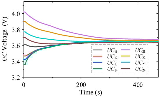
Figure 16.
The Multi-stacked buck-boost based equalizer balance eight series-connected UCs in Case 1.
Case 2: Figure 17 demonstrates a marked voltage convergence for the eight UCs. Starting from a significant imbalance (3.6670, 3.7870, 3.9140, 4.0320, 3.3430, 3.4105, 3.4985, 3.5880 V), a 350 s equalization phase successfully brought the voltages to 3.6485, 3.6655, 3.6660, 3.6650, 3.6645, 3.6485, 3.6390, and 3.6355 V. The result was a drastic reduction in the maximum voltage difference, from an initial 0.6890 V to a final 0.030 V.
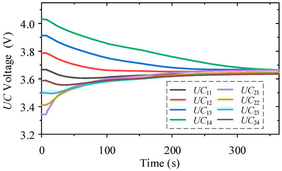
Figure 17.
The multi-stacked buck-boost based equalizer balance eight series-connected UCs in Case 2.
Case 3: The voltage change in the batteries during charging is shown in Figure 18. The UC cells’ initial voltages are 3.5650, 3.9750, 3.8560, 3.6550, 3.3830, 3.7615, 3.4590, and 3.5835V, respectively. After about 1000s of charging balance, the voltages become 3.6425, 3.6725, 3.6640, 3.6585, 3.6655, 3.6520, 3.6390, and 3.6375V. The maximum voltage difference reduces from 0.5920V to 0.035 V. The results show that the voltages gradually tend to be consistent.
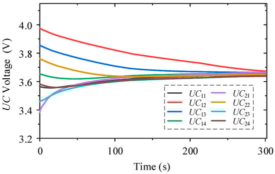
Figure 18.
The multi-stacked buck-boost based equalizer balance eight series-connected UCs in Case 3.
The measured system efficiency is illustrated in Figure 19. When the output power is 10–35 W, the system efficiency is about 87.5%.
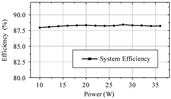
Figure 19.
The multi-stacked buck-boost based equalizer balance eight series-connected UCs in Case 4.
4. Comparison with Conventional Voltage Equalizers
This study models an 8-cell series string. The bidirectional switches, each combining two MOSFETs in inverse parallel, are driven by a single circuit. Since all battery systems require a charger/discharger as an essential component, Table 2 compares only the number of additional components needed for the balancing circuit. Components required for the charge/discharge system itself are excluded from this count. The component requirements, such as the number of MOSFETs, inductors, and capacitors, of the proposed design are benchmarked against prior equalizers in Table 2.
Table 2.
Comparison of proposed equalizer in terms of components.
The performance evaluation framework in Table 3 encompasses five comparison categories: control logic (CL), balance speed (BS), scalability, current stress, and system efficiency. A brief description of each characteristic is provided below.
Table 3.
Performance comparison between the multi-stacked buck-boost based equalizer and existing.
- Control Logic: The control logics are primarily classified into two categories. The first method (VB) involves activating the balancing function by controlling switch conduction based on measured cell voltages. The second method (Auto) achieves automatic cell voltage convergence by utilizing either a fixed-frequency/pulse-width PWM signal or the inherent ripple current from the charging process as the driving mechanism.
- Balance Speed: This refers to the convergence speed of a balancing system under a given voltage difference. A faster balance speed enables the system to reach its balancing target more quickly. Balance speeds are typically classified into several grades: Very Fast (VF), Fast (F), Medium (M), and Slow (S).
- Scalability: This refers to the system’s capability to be cost-effectively adapted for use with a long battery string while maintaining its balancing functionality. Scalability is typically classified into several grades: Excellent (E), Good (G), and Medium (M).
- Current Stress: Current stress refers to the current stress on individual cells during the series battery cell equalization process. Whether in integrated or self-equalizing circuits, the impact of charging current must be considered. Scalability is generally categorized into several levels: Large (L), Medium (M), and Small (S).
- Efficiency: The balancing efficiency of a self-balancing circuit refers to the effectiveness of the conversion and transfer process during which “balancing energy” is delivered from higher-energy cells to lower-energy ones. The integrated balancing efficiency refers to the effectiveness of energy distribution from the power source to each individual cell.
5. Conclusions
A symmetric multi-boost-buck circuit for an integrated equalizer is proposed. Derived from the principle of current ripple in a boost converter, the symmetric structure ensures that each cell has an independent current path during balancing, which minimizes the current stress on individual cells. Additionally, the use of inductors instead of diodes significantly boosts the equalization efficiency under low voltage conditions. The proposed integrated equalization circuit was experimentally validated under various voltage distributions, with results demonstrating good voltage convergence performance.
A key challenge for future research is to extend this topology to long battery strings while maintaining the current voltage and current ratings of the components, in order to achieve effective charging balance and discharging balance.
Author Contributions
Conceptualization, Y.Q., X.P. and Z.W.; methodology, Y.Q., M.M. and Y.O.; investigation, Y.Q., M.M. and Y.O.; software, W.X. and X.L.; validation, W.X. and X.L.; writing—original draft preparation, Y.Q. and W.X.; writing—review and editing, Z.W. and X.Z. All authors have read and agreed to the published version of the manuscript.
Funding
This work was supported by the Science and Technology Project of the State Grid Sichuan Electric Power Company. The project is titled “Friendly Distributed Energy Storage Collaborative Technology and Application Considering the Differentiated Demand Coupling of New Distribution Network”. The project number is 521996240006.
Data Availability Statement
The original contributions presented in this study are included in the article. Further inquiries can be directed to the corresponding author.
Conflicts of Interest
Y.Q., X.L. and W.X. were employed by State Grid Sichuan Electric Power Company. X.P., M.M. and Y.O. were employed by State Grid Tianfu New Area Power Supply Company. The remaining authors declare that the research was conducted in the absence of any commercial or financial relationships that could be construed as a potential conflict of interest.
References
- Li, J.; Fang, Z.; Wang, Q.; Zhang, M.; Li, Y.; Zhang, W. Optimal Operation with Dynamic Partitioning Strategy for Centralized Shared Energy Storage Station with Integration of Large-scale Renewable Energy. J. Mod. Power Syst. Clean Energy 2024, 12, 359–370. [Google Scholar] [CrossRef]
- Chen, X.; Yang, Y.; Song, J.; Wang, J.; He, G. Hybrid Energy Storage System Optimization with Battery Charging and Swapping Coordination. IEEE Trans. Autom. Sci. Eng. 2023, 21, 4094–4105. [Google Scholar] [CrossRef]
- Chen, K.; Liu, L.; Zang, T.; Zhou, Y.; Yan, Z.; Xu, Y.; Xu, B.; Zhang, P.; Cai, C. Double-Layer Multi winding Transformer-Based Modular-Integrated Equalizer for Extended Battery String. IEEE Trans. Power Electron. 2023, 39, 2767–2776. [Google Scholar] [CrossRef]
- Jiang, Y.; Ke, Y.; Yang, F.; Ji, J.; Peng, W. State of Health Estimation for Second-Life Lithium-Ion Batteries in Energy Storage System with Partial Charging-Discharging Workloads. IEEE Trans. Ind. Electron. 2024, 71, 13178–13188. [Google Scholar] [CrossRef]
- Rasheed, M.; Hassan, R.; Kamel, M.; Wang, H.; Zane, R.; Tong, S.; Smith, K. Active Reconditioning of Retired Lithium-Ion Battery Packs from Electric Vehicles for Second-Life Applications. IEEE J. Emerg. Sel. Top. Power Electron. 2023, 12, 388–404. [Google Scholar] [CrossRef]
- Hu, X.; Deng, X.; Wang, F.; Deng, Z.; Lin, X.; Teodorescu, R.; Pecht, M.G. A Review of Second-Life Lithium-Ion Batteries for Stationary Energy Storage Applications. Proc. IEEE 2022, 110, 735–753. [Google Scholar] [CrossRef]
- Xu, B.; Yan, Z.; Xiong, L.; Zhang, L.; Zhou, W.; Mai, R.; He, Z.; Liu, L. A Double-Switch Single-Transformer Integrated Equalizer for the Recycled Power Battery String of Automatic Guided Vehicles. IEEE Trans. Ind. Electron. 2022, 70, 2596–2606. [Google Scholar] [CrossRef]
- Gallardo-Lozano, J.; Romero-Cadaval, E.; Milanes-Montero, M.I.; Guerrero-Martinez, M.A. Battery equalization active methods. J. Power Sources 2014, 246, 934–949. [Google Scholar] [CrossRef]
- Shang, Y.; Xia, B.; Lu, F.; Zhang, C.; Cui, N.; Mi, C.C. A Switched Coupling-Capacitor Equalizer for Series-Connected Battery Strings. IEEE Trans. Power Electron. 2017, 32, 7694–7706. [Google Scholar] [CrossRef]
- Ye, Y.; Cheng, K.W.E. Modeling and Analysis of series–parallel switched-capacitor voltage equalizer for battery/supercapacitor strings. IEEE J. Emerg. Sel. Top. Power Electron. 2015, 3, 977–983. [Google Scholar] [CrossRef]
- Zhou, G.; Zhang, X.; Gao, K.; Tian, Q.; Xu, S. Two-Mode Active Balancing Circuit Based on Switched-Capacitor and Three-Resonant-State LC Units for Series-Connected Cell Strings. IEEE Trans. Ind. Electron. 2021, 69, 4845–4858. [Google Scholar] [CrossRef]
- Lee, S.-W.; Lee, K.-M.; Choi, Y.-G.; Kang, B. Modularized Design of Active Charge Equalizer for Li-Ion Battery Pack. IEEE Trans. Ind. Electron. 2018, 65, 8697–8706. [Google Scholar] [CrossRef]
- Xu, G.; Chen, E.; Liu, F.; Liu, Y.; Xiong, W.; Su, M. Multicell-to-Multicell Equalizer with Hybrid Pulsewidth Modulation and Phase-Shift Modulation. IEEE Trans. Power Electron. 2023, 39, 4400–4411. [Google Scholar] [CrossRef]
- Wang, S.; Wang, Y.; Chen, G.; Wei, D.; Shang, Y. An Efficient and Compact Equalizer Based on Forward-Flyback Conversion for Large-Scale Energy Storage Systems. IEEE Trans. Transp. Electrif. 2023, 10, 1222–1232. [Google Scholar] [CrossRef]
- Liu, L.; Yan, Z.; Xu, B.; Zhang, P.; Cai, C.; Yang, H. A Highly Scalable Integrated Voltage Equalizer Based on Parallel-Transformers for High-Voltage Energy Storage Systems. IEEE Trans. Ind. Electron. 2023, 71, 595–603. [Google Scholar] [CrossRef]
- Zou, R.; Liu, F.; Liu, Y.; Xu, G.; Liu, F. An LLC-Based Battery Equalizer with Inherent Current Limitation. IEEE Trans. Power Electron. 2021, 37, 1828–1840. [Google Scholar] [CrossRef]
- Qi, X.; Wang, Y.; Fang, M.; Wang, H.; Wang, Y.; Chen, Z. A Family of Integrated Cascade Multiport Converters for Centralized Equalization Systems: Derivation, Analysis, and Verification. IEEE Trans. Power Electron. 2023, 38, 7398–7415. [Google Scholar] [CrossRef]
- Qi, X.; Wang, Y.; Fang, M. An Integrated Cascade Structure-Based Isolated Bidirectional DC–DC Converter for Battery Charge Equalization. IEEE Trans. Power Electron. 2020, 35, 12003–12021. [Google Scholar] [CrossRef]
- Wei, Z.; Wang, H.; Lu, Y.; Shu, D.; Ning, G.; Fu, M. Bidirectional Constant Current String-to-Cell Battery Equalizer Based on L2C3 Resonant Topology. IEEE Trans. Power Electron. 2022, 38, 666–677. [Google Scholar] [CrossRef]
- Peng, F.; Wang, H.; Wei, Z. An LLC-Based Highly Efficient S2M and C2C Hybrid Hierarchical Battery Equalizer. IEEE Trans. Power Electron. 2019, 35, 5928–5937. [Google Scholar] [CrossRef]
- Uno, M.; Yashiro, K.; Hasegawa, K. Modularized Equalization Architecture with Voltage Multiplier-Based Cell Equalizer and Switchless Switched Capacitor Converter-Based Module Equalizer for Series-Connected Electric Double-Layer Capacitors. IEEE Trans. Power Electron. 2018, 34, 6356–6368. [Google Scholar] [CrossRef]
- Mai, R.; Xu, B.; Yan, Z.; Zhou, W.; Liu, L. A Compact-Size Multi-Winding Transformer-Based Discharge Equalizer for Electric Two-Wheelers and Three-Wheelers Vehicles Power Battery. IEEE Trans. Veh. Technol. 2022, 71, 4889–4897. [Google Scholar] [CrossRef]
- Yang, X.; Qi, Y.; Liu, J.; Jia, Z.; Wang, D. Bidirectional Converter Integrating Voltage Equalizer Based on Symmetrical Voltage Multiplier by Sharing a Magnetic Component for Series-Connected Cells. IEEE Trans. Transp. Electrif. 2021, 7, 1074–1087. [Google Scholar] [CrossRef]
- Liu, L.; Li, B.; Xu, Y.; Wang, W.; Zang, T.; Zhou, Y.; Zhang, P. A Multiple-Receiver-IPT-Based Voltage Equalizer With Voltage Doublers for Battery-String Charging. IEEE J. Emerg. Sel. Top. Power Electron. 2025, 13, 1339–1348. [Google Scholar] [CrossRef]
- Zhang, P.; Zhang, T.; Yu, X.; Yuan, Z.; Cai, C.; Lin, H.; Xu, Y.; Liu, L. An LCC Wireless Charger with Embedded Cell Equalization via a Shared Compensation Inductor. IEEE Trans. Power Electron. 2025, 1–10. [Google Scholar] [CrossRef]
- Fu, M.; Zhao, C.; Song, J.; Ma, C. A Low-Cost Voltage Equalizer Based on Wireless Power Transfer and a Voltage Multiplier. IEEE Trans. Ind. Electron. 2017, 65, 5487–5496. [Google Scholar] [CrossRef]
- Pascual, C.; Krein, P.T. Switched capacitor system for automatic series battery equalization. In Proceedings of the APEC 97—Applied Power Electronics Conference, Atlanta, GA, USA, 27 February 1997; Volume 2, pp. 848–854. [Google Scholar]
- Ye, Y.; Cheng, K.W.E. Analysis and Design of Zero-Current Switching Switched-Capacitor Cell Balancing Circuit for Series-Connected Battery/Supercapacitor. IEEE Trans. Veh. Technol. 2017, 67, 948–955. [Google Scholar] [CrossRef]
- Shang, Y.; Cui, N.; Duan, B.; Zhang, C. Analysis and Optimization of Star-Structured Switched-Capacitor Equalizers for Series-Connected Battery Strings. IEEE Trans. Power Electron. 2017, 33, 9631–9646. [Google Scholar] [CrossRef]
- Wei, Z.; Peng, F.; Wang, H. An LCC Based String-to-Cell Battery Equalizer with Simplified Constant Current Control. IEEE Trans. Power Electron. 2021, 37, 1816–1827. [Google Scholar] [CrossRef]
- Xu, B.; Yan, Z.; Zhou, W.; Zhang, L.; Yang, H.; Liu, Y.; Liu, L. A Bidirectional Integrated Equalizer Based on the Buck-boost converter–Zeta Converter for Hybrid Energy Storage System. IEEE Trans. Power Electron. 2022, 37, 12659–12668. [Google Scholar] [CrossRef]
- Uno, M.; Kukita, A. Single-Switch Single-Transformer Cell Voltage Equalizer Based on Forward–Flyback Resonant Inverter and Voltage Multiplier for Series-Connected Energy Storage Cells. IEEE Trans. Veh. Technol. 2014, 63, 4232–4247. [Google Scholar] [CrossRef]
- Uno, M.; Hasegawa, K. Modular Equalization System Based on Star-Connected Phase-Shift Switched Capacitor Converters with Inherent Constant Current Characteristics for Electric Double-Layer Capacitor Modules. IEEE Trans. Power Electron. 2020, 35, 10271–10284. [Google Scholar] [CrossRef]
- Zhang, P.; Yu, X.; Yang, Q.; Li, Z.; Yuan, Z.; Cai, C.; Lin, H.; Xu, Y.; Liu, L. Dual-Layer Equalization Architecture for Anti-misalignment Capability Enhancement in Multiple-Receiver-Based WPT Equalizer. IEEE Trans. Power Electron. 2024, 39, 14027–14038. [Google Scholar] [CrossRef]
- Cai, C.; Wang, J.; Luo, Y.; Rao, Y.; Zhang, P.; Zang, T.; Lin, H.; Liu, L. Multi-State Voltage Balancing of UAV’s Cell String: A Reconfigurable WPT Based Multiport Hybrid Charging Approach. IEEE Trans. Ind. Electron. 2024, 72, 266–277. [Google Scholar] [CrossRef]
- Liu, L.; Chen, K.; Xu, Y.; Zang, T.; Zhou, Y.; Xiong, L.; Xu, B.; Zhang, P.; Cai, C. Modular Equalization System Based on Double-Layer Voltage Multipliers for Series-Connected Ultra-Capacitors String. IEEE J. Emerg. Sel. Top. Power Electron. 2023, 12, 3280–3289. [Google Scholar] [CrossRef]
- Uno, M.; Tanaka, K. Single-Switch Cell Voltage Equalizer Using Multistacked Buck-Boost Converters Operating in Discontinuous Conduction Mode for Series-Connected Energy Storage Cells. IEEE Trans. Veh. Technol. 2011, 60, 3635–3645. [Google Scholar] [CrossRef]
- Uno, M.; Xu, Q.; Sato, Y. Multi-Stacked Superbuck Converter-Based Single-Switch Charger Integrating Cell Voltage Equalizer for Series-Connected Energy Storage Cells. Energies 2022, 15, 3619. [Google Scholar] [CrossRef]
Disclaimer/Publisher’s Note: The statements, opinions and data contained in all publications are solely those of the individual author(s) and contributor(s) and not of MDPI and/or the editor(s). MDPI and/or the editor(s) disclaim responsibility for any injury to people or property resulting from any ideas, methods, instructions or products referred to in the content. |
© 2025 by the authors. Licensee MDPI, Basel, Switzerland. This article is an open access article distributed under the terms and conditions of the Creative Commons Attribution (CC BY) license (https://creativecommons.org/licenses/by/4.0/).