
Enhanced Simulation Accuracy and Design Optimization in Power Semiconductors Through Individual Aluminum Metallization Layer Modeling


Abstract
1. Introduction
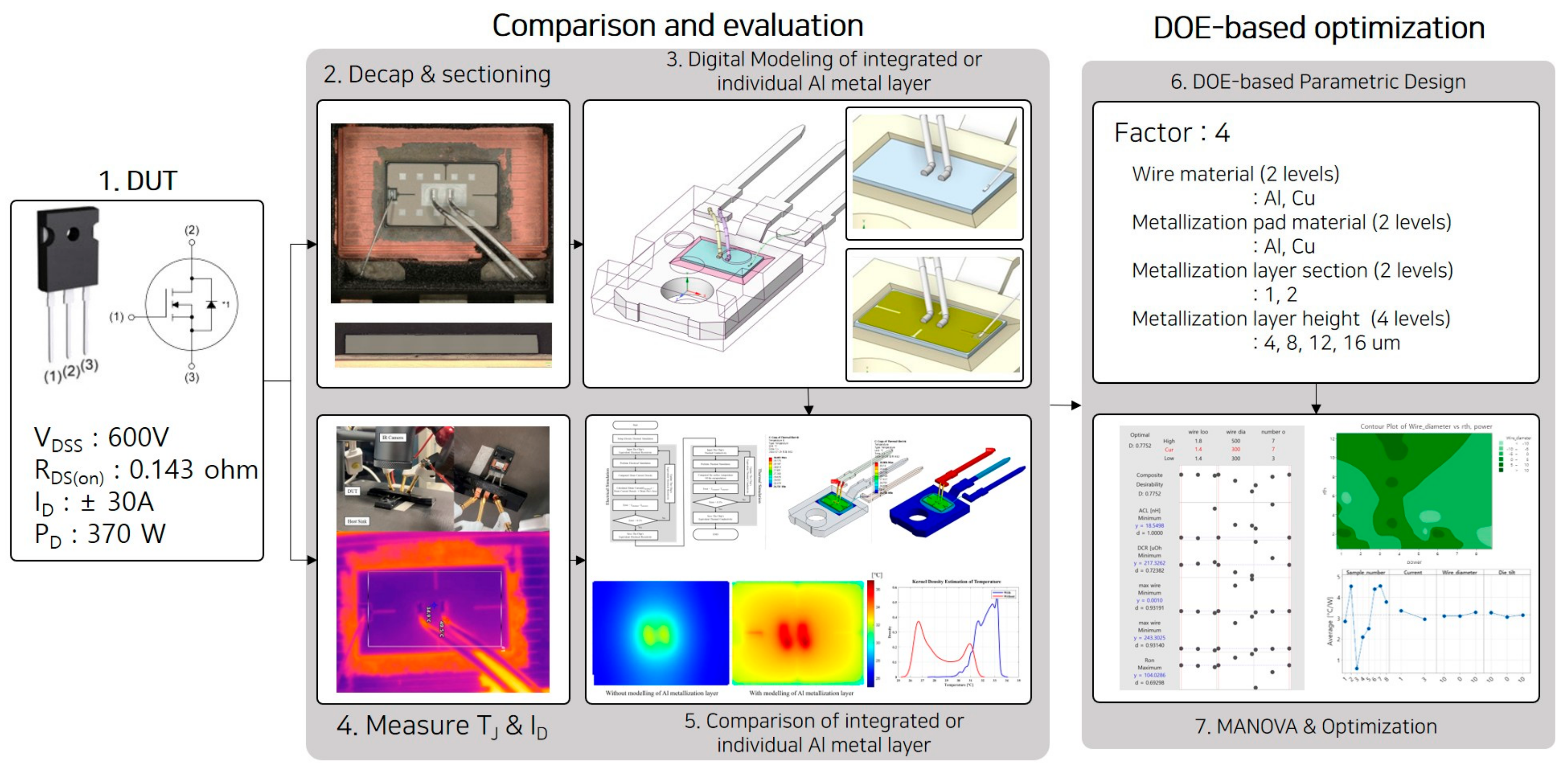
2. Comparison and Evaluation of Integrated vs. Individual Al Metallization Layer Modeling Approaches
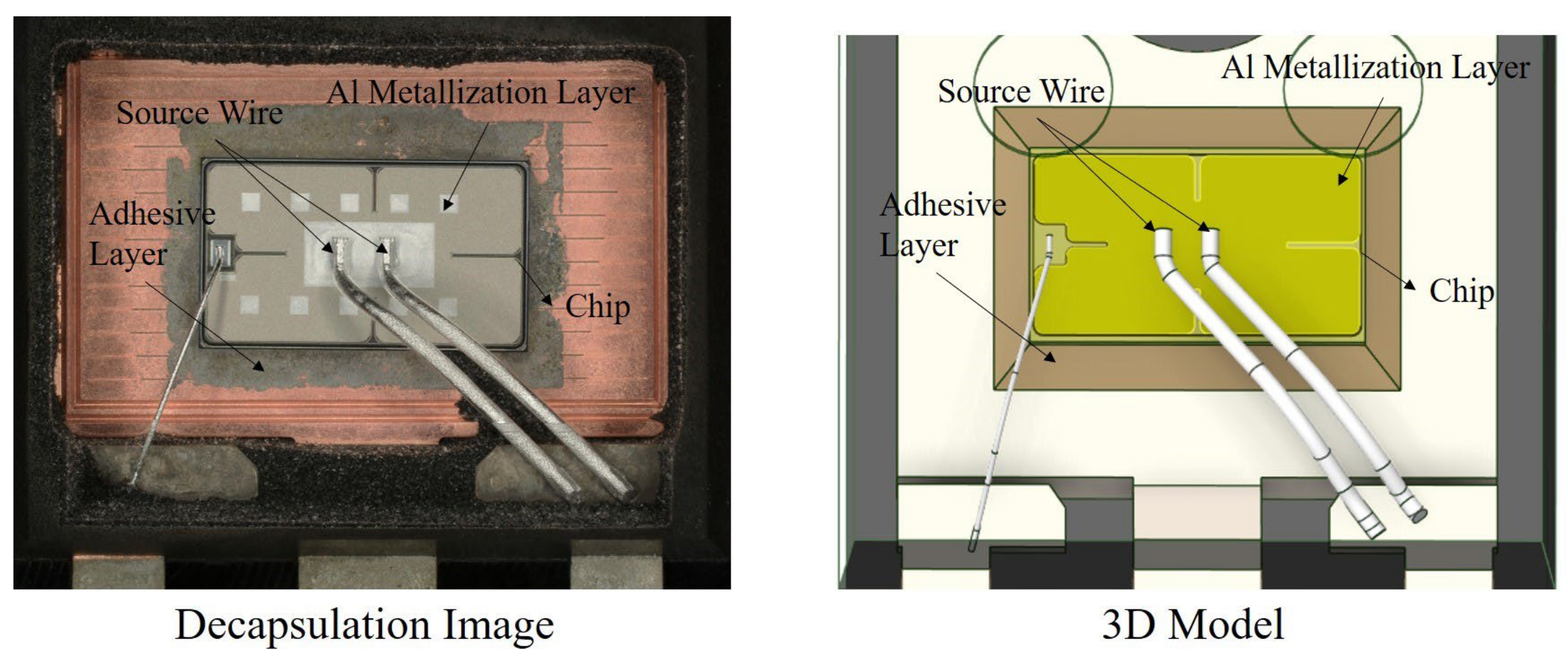
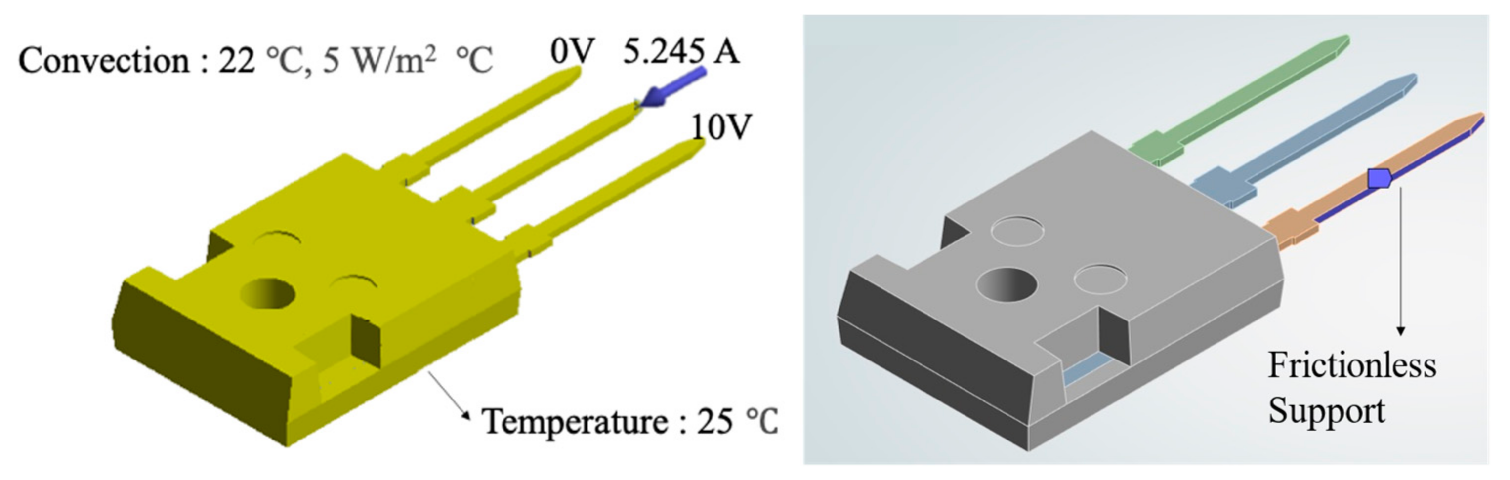
2.1. Preparation and Test
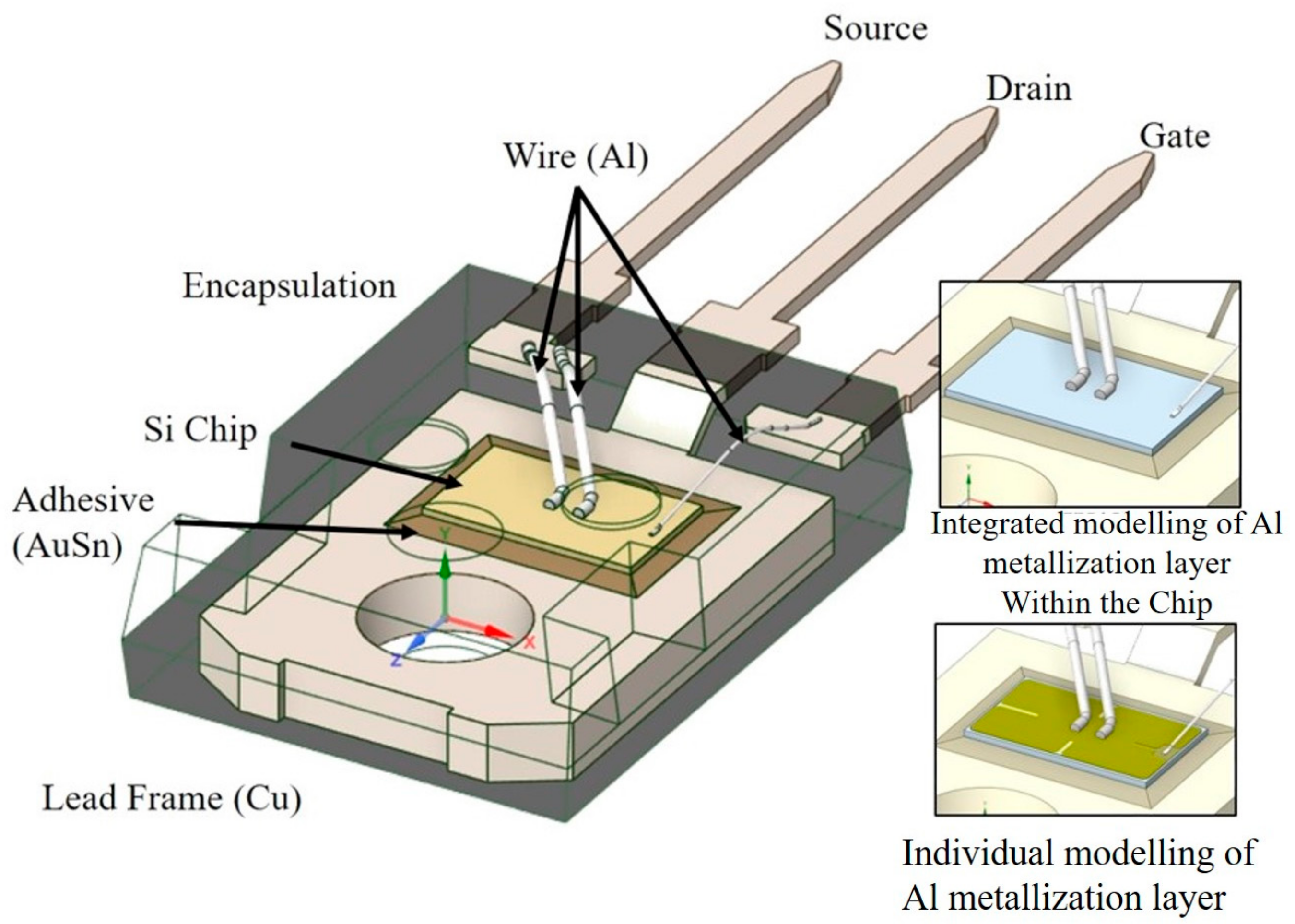
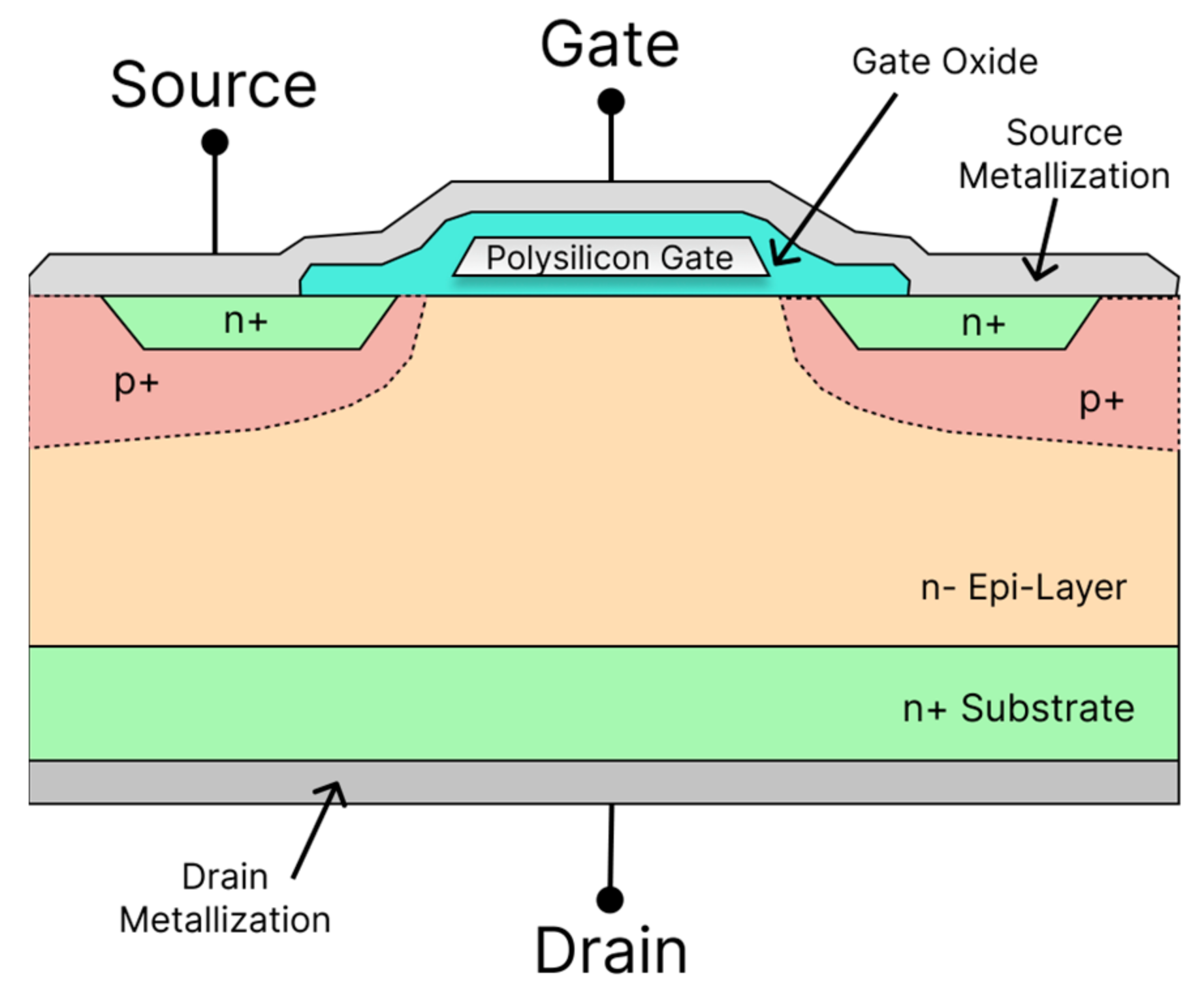
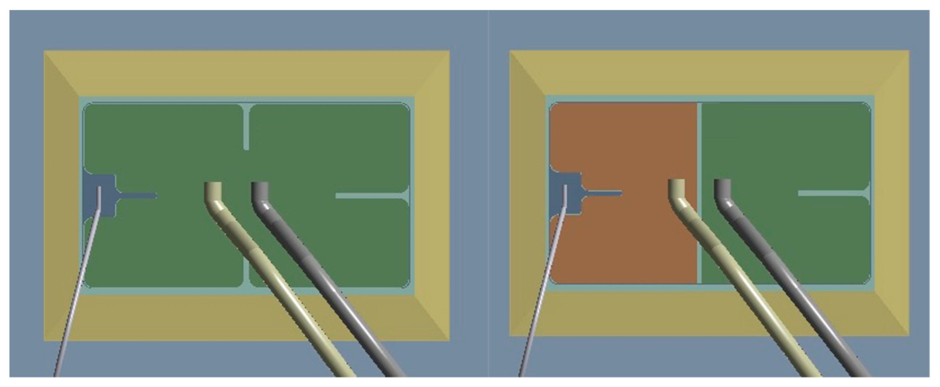
2.2. 3D Geometry
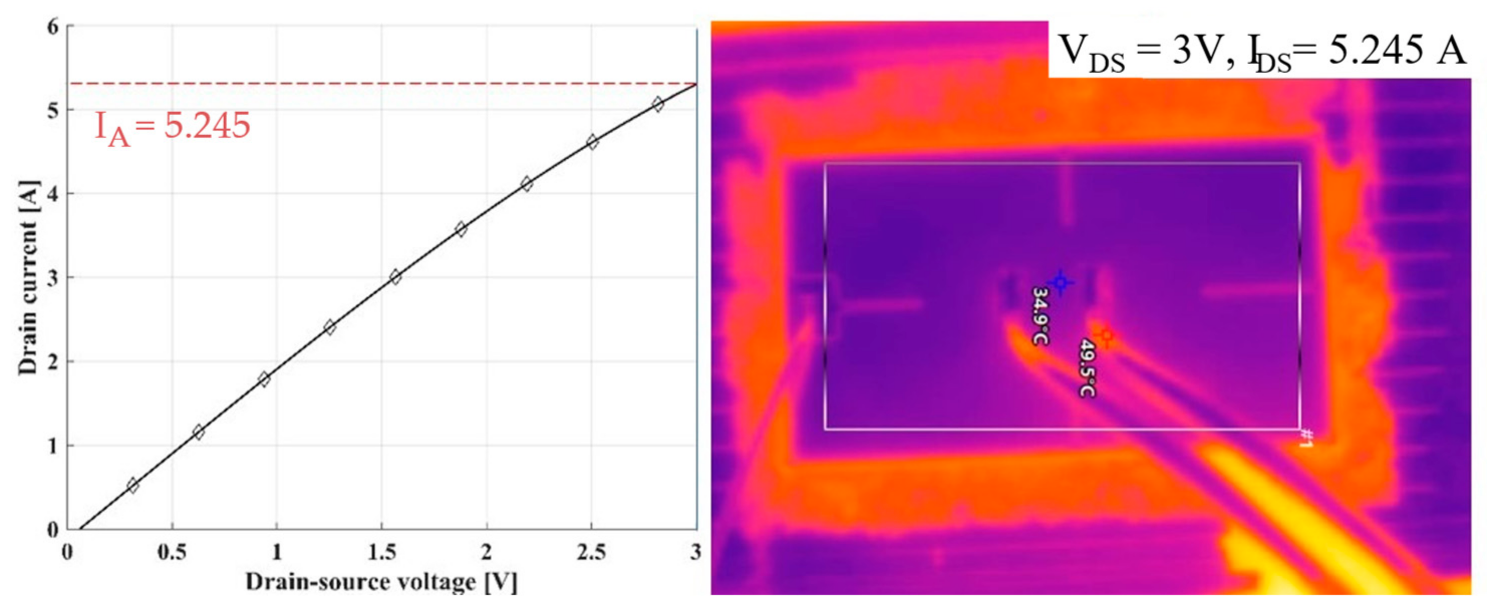
2.3. Measurement of Junction Temperature & Drain Current
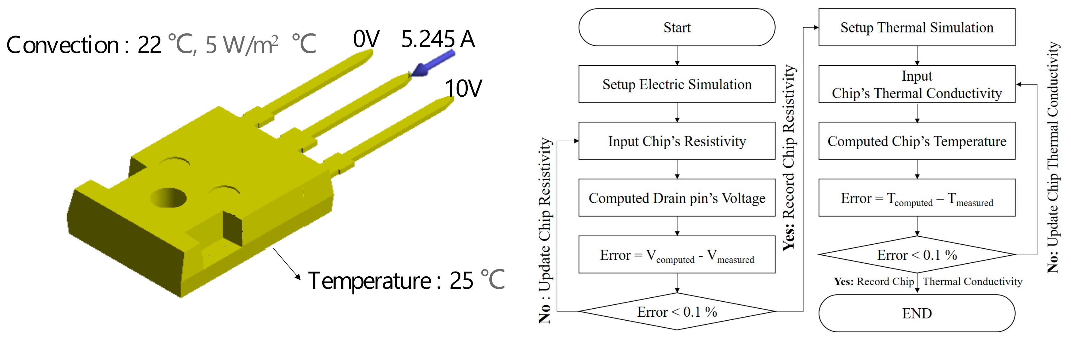
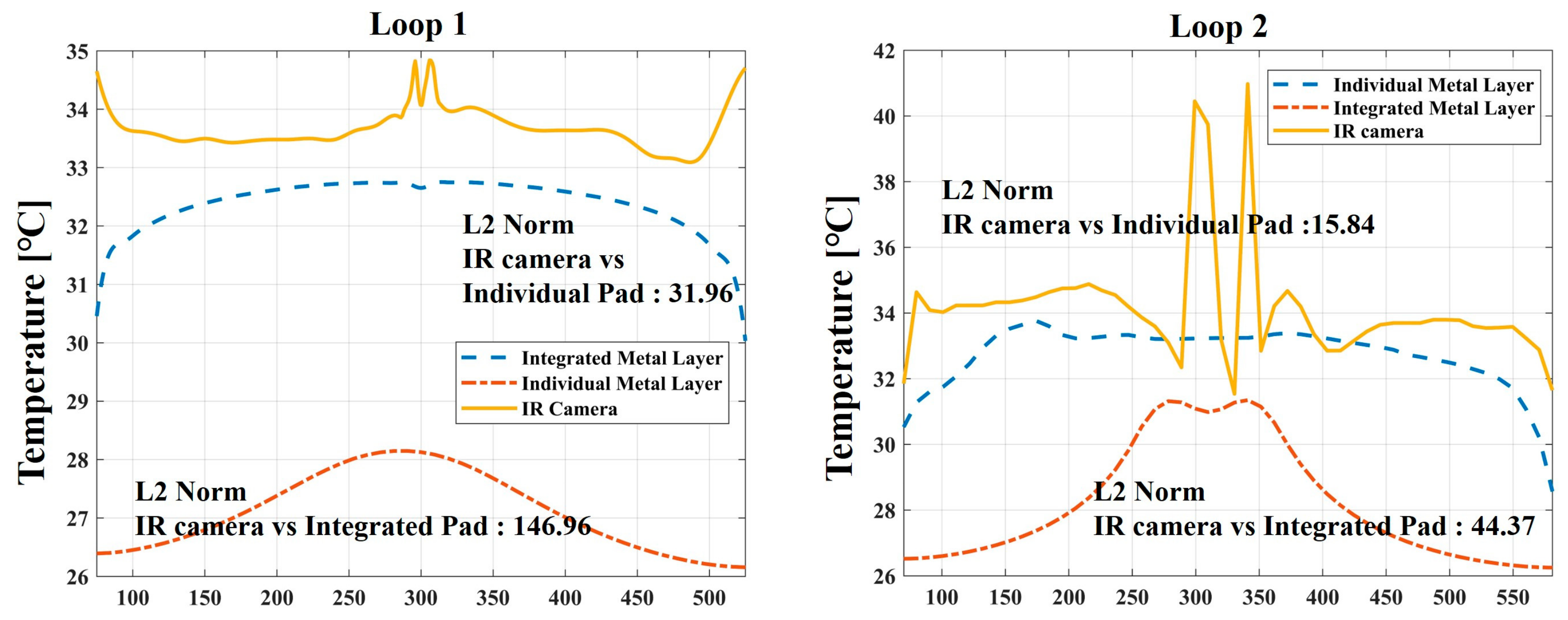
2.4. Calibration of FEM Model Using Experimental Data
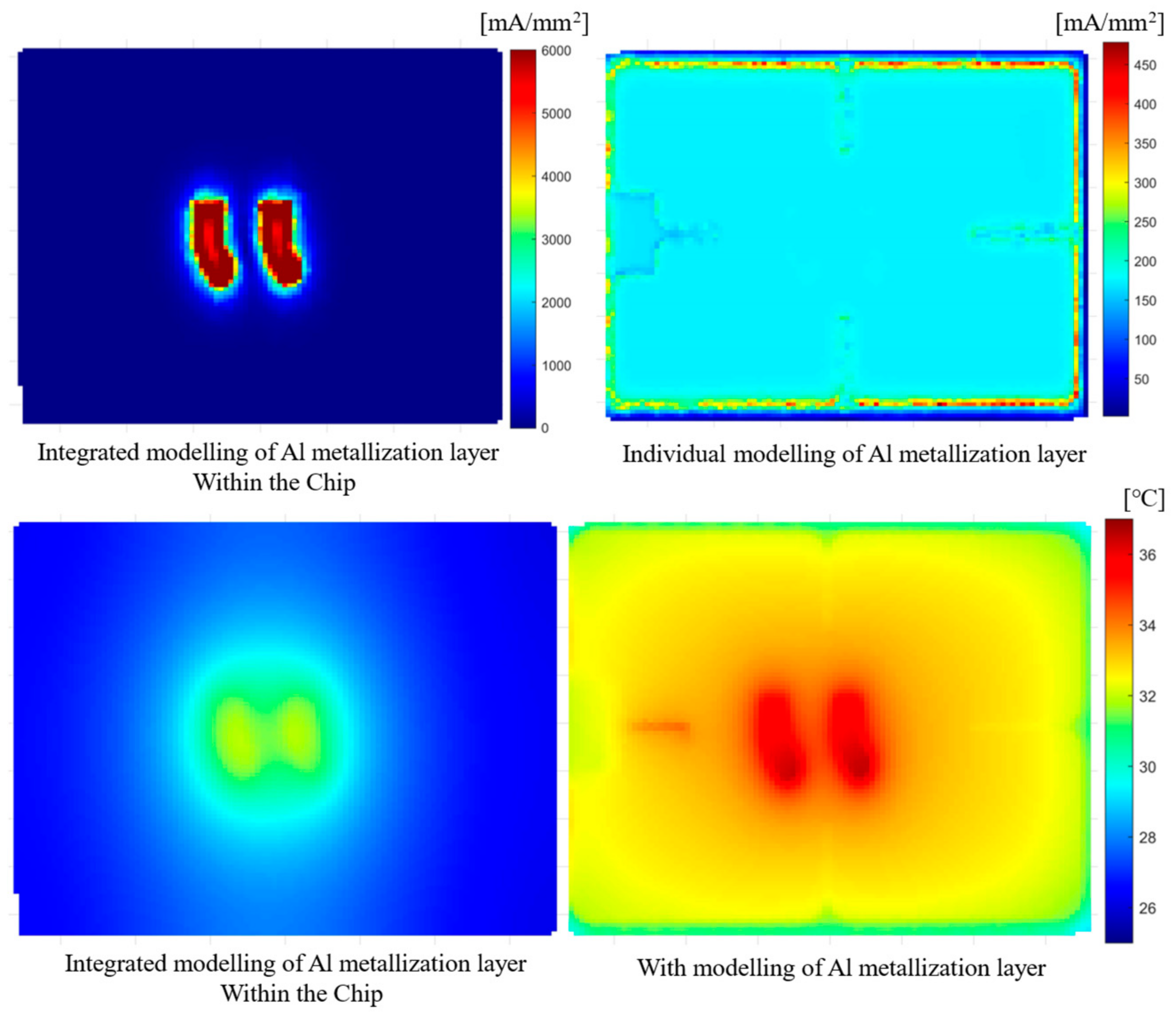
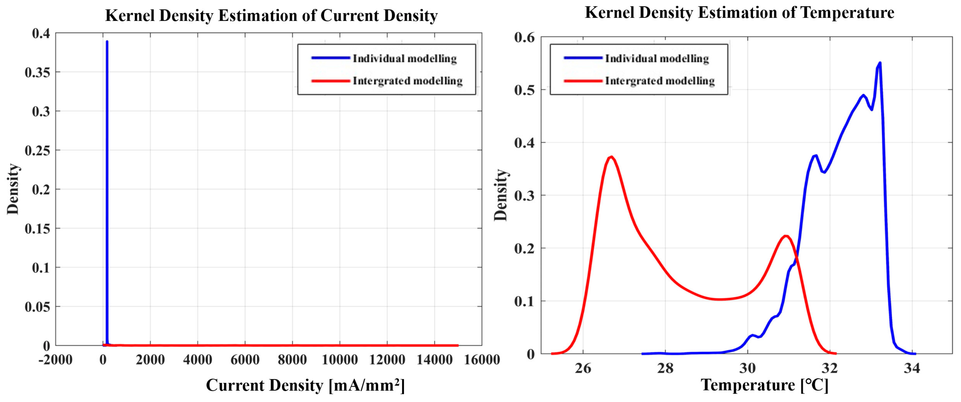
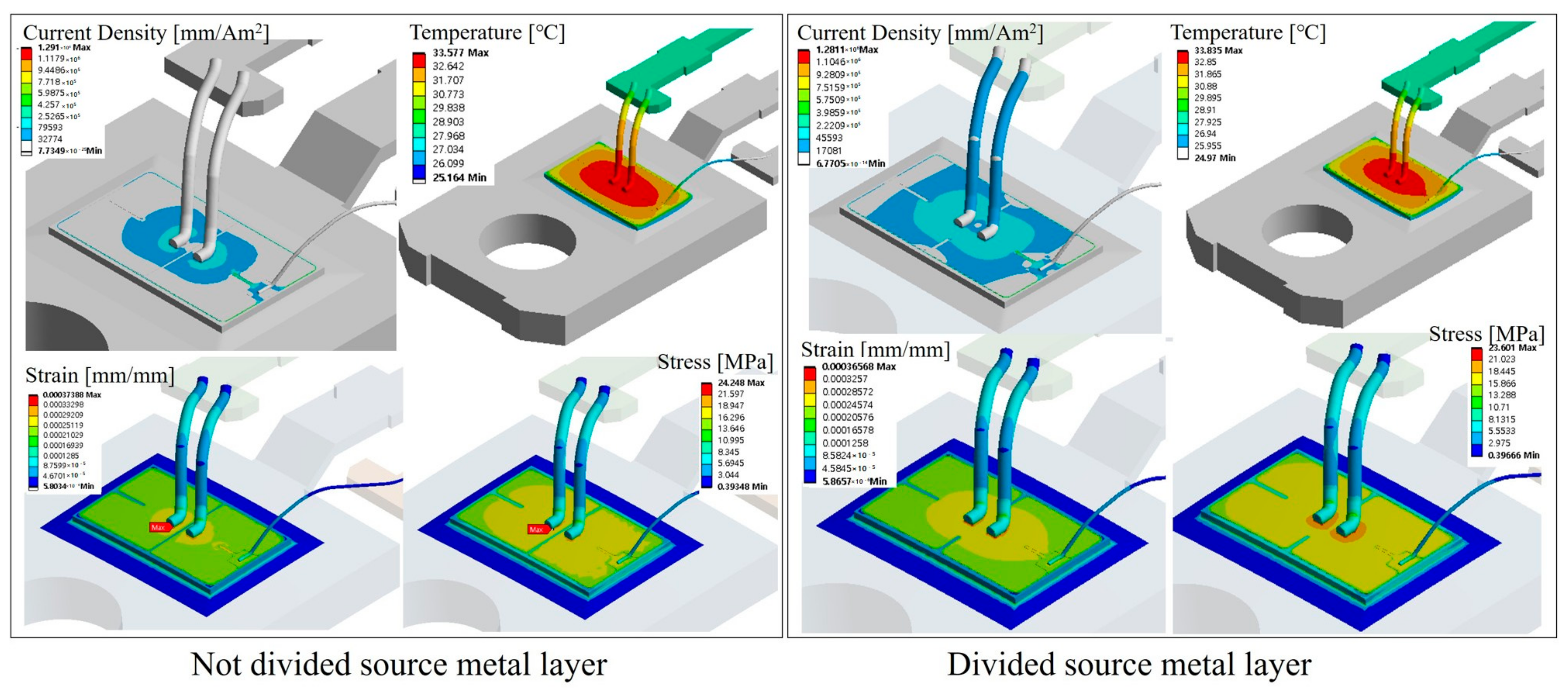
2.5. Results and Discussion
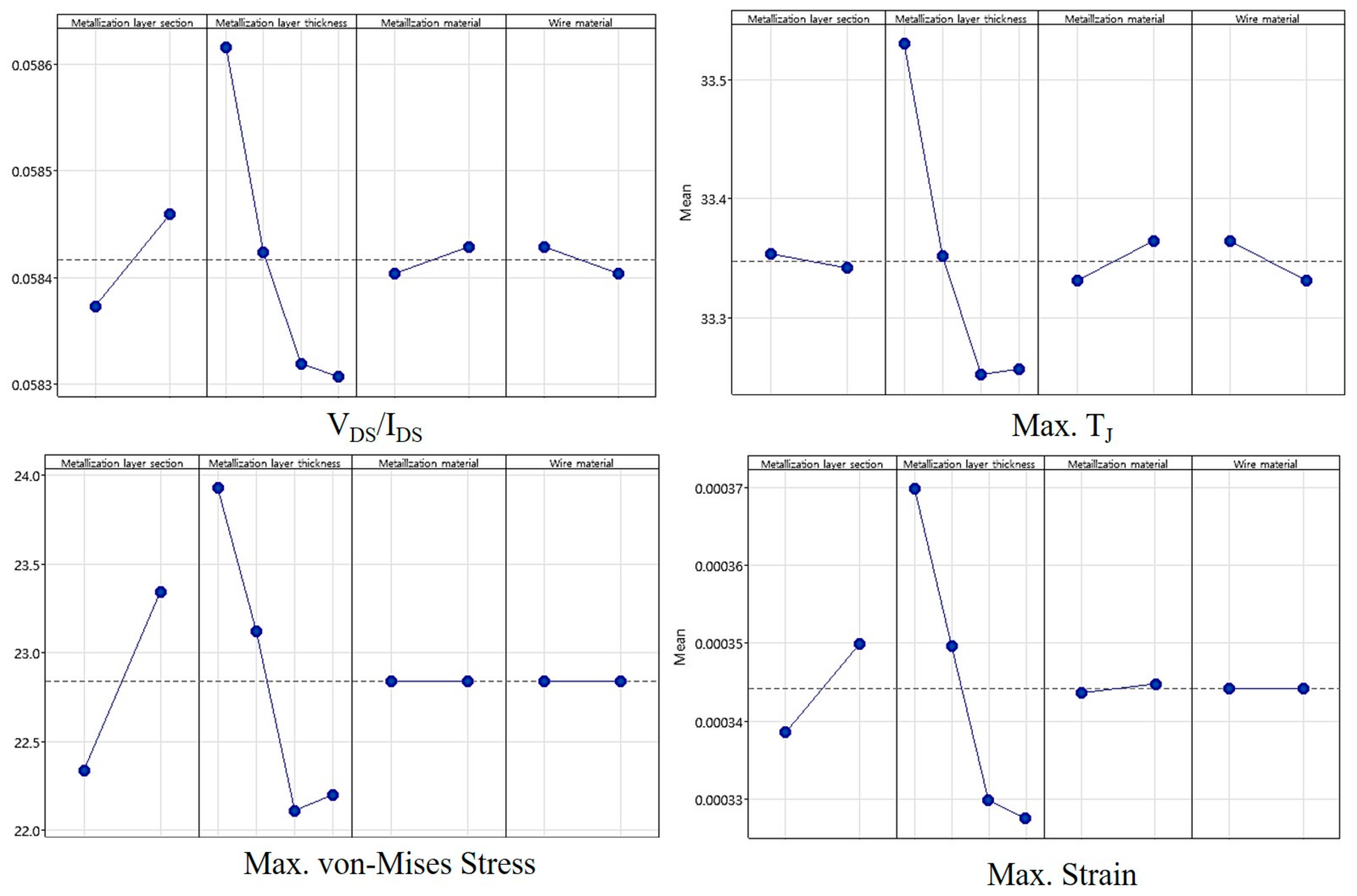
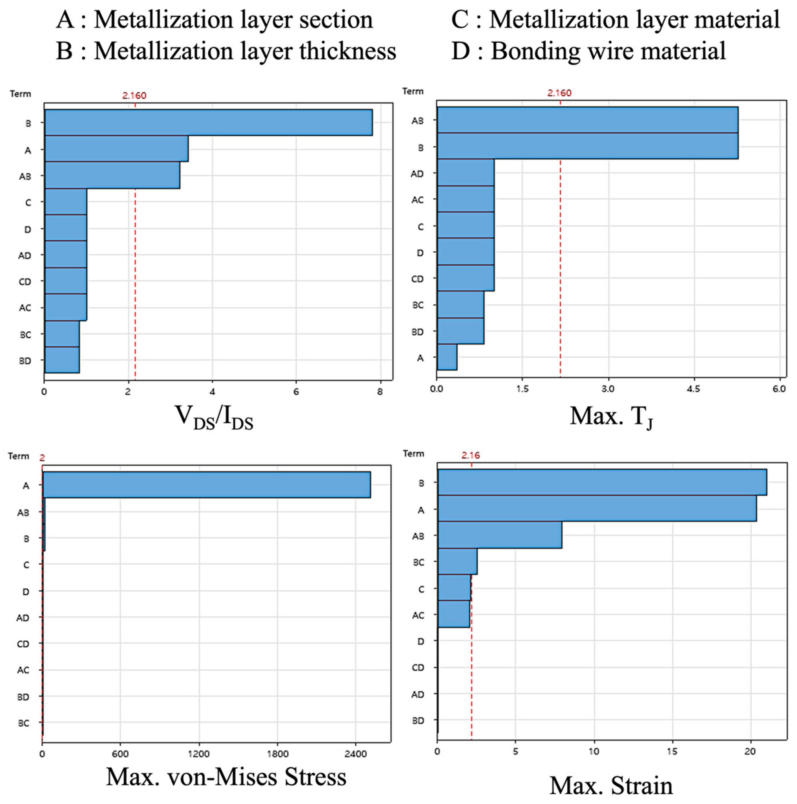
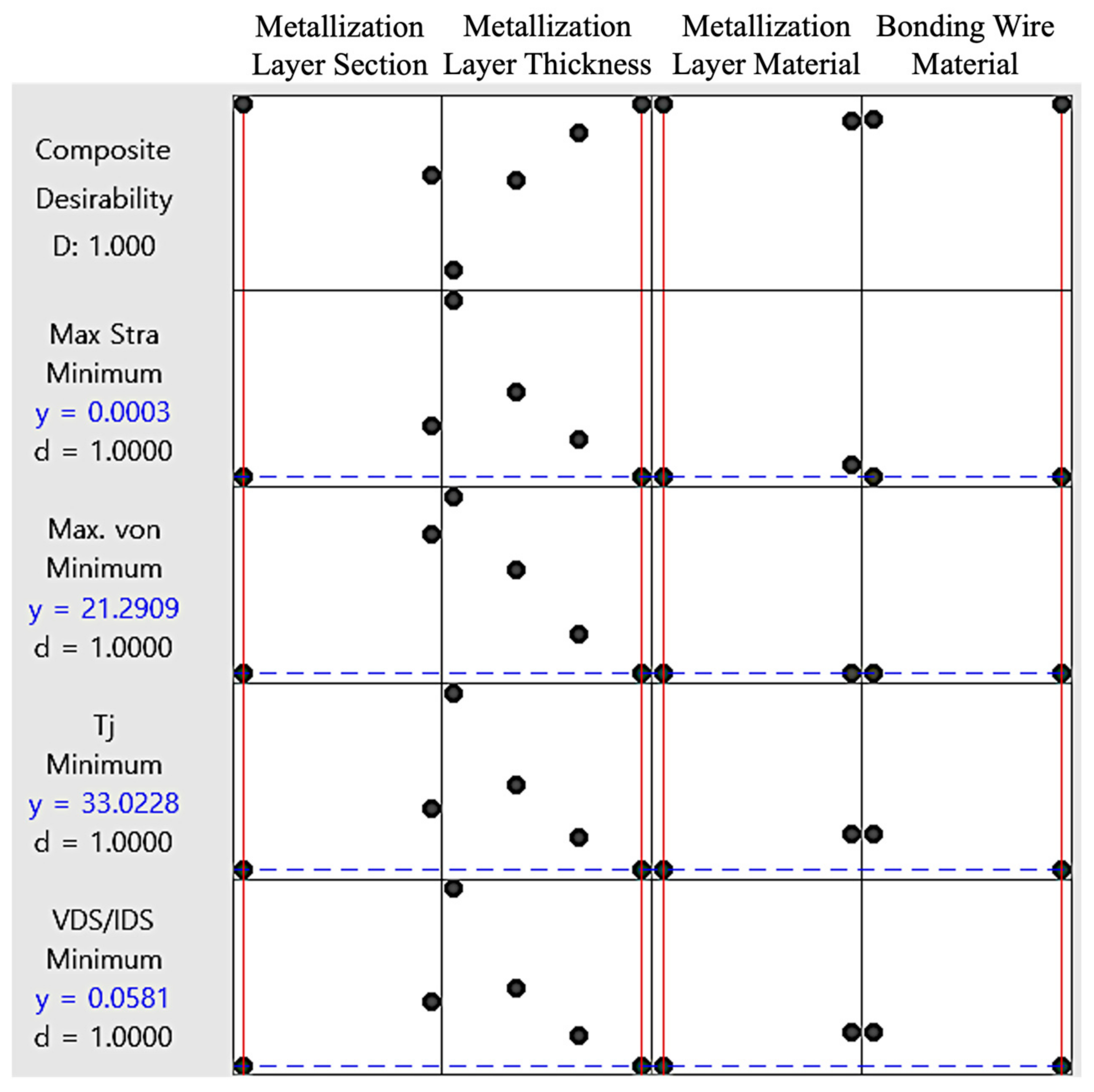
3. Optimal Design for Wire and Metallization Layer Variations
3.1. Setup and Factor Analysis for Metallization Layer and Bonding Wire Optimization
3.2. Results and Discussion
4. Conclusions
Author Contributions
Funding
Data Availability Statement
Conflicts of Interest
References
- Blaabjerg, F.; Wang, H.; Vernica, I.; Liu, B.; Davari, P. Reliability of Power Electronic Systems for EV/HEV Applications. Proc. IEEE 2021, 109, 1060–1076. [Google Scholar] [CrossRef]
- Calabretta, M.; Renna, M.; Vinciguerra, V.; Messina, A.A. Power Packages Interconnections for High Reliability Automotive Applications. In Proceedings of the ESSDERC 2019—49th European Solid-State Device Research Conference (ESSDERC), Cracow, Poland, 23–26 September 2019; pp. 35–39. [Google Scholar] [CrossRef]
- Wang, Y.; Ding, Y.; Yin, Y. Reliability of Wide Band Gap Power Electronic Semiconductor and Packaging: A Review. Energies 2022, 15, 6670. [Google Scholar] [CrossRef]
- Li, Q.; Li, Y.-B.; Fu, H.-D.; Tu, C.-M.; Xiao, B.; Xiao, F.; Zhai, D.-Y.; Lu, J.-W. Review of the Failure Mechanism and Methodologies of IGBT Bonding Wire. IEEE Trans. Compon. Packag. Manuf. Technol. 2023, 13, 1045–1057. [Google Scholar] [CrossRef]
- Ye, H.; Lin, M.; Basaran, C. Failure modes and FEM analysis of power electronic packaging. Finite Elem. Anal. Des. 2002, 38, 601–612. [Google Scholar] [CrossRef]
- Otiaba, K.C.; Bhatti, R.; Ekere, N.; Mallik, S.; Ekpu, M. Finite element analysis of the effect of silver content for Sn–Ag–Cu alloy compositions on thermal cycling reliability of solder die attach. Eng. Fail. Anal. 2013, 28, 192–207. [Google Scholar] [CrossRef]
- Celaya, J.R.; Saxena, A.; Saha, S.; Goebel, K.F. Prognostics of power MOSFETs under thermal stress accelerated aging using data-driven and model-based methodologies. Annu. Conf. PHM Soc. 2011, 3, 1. [Google Scholar] [CrossRef]
- Naghibi, J.; Mehran, K.; Foster, M.P. An online failure assessment approach for SiC-based MOSFET power modules using iterative condition monitoring technique. In Proceedings of the 2020 IEEE 21st Workshop on Control and Modeling for Power Electronics (COMPEL), Aalborg, Denmark, 9–12 November 2020; pp. 1–5. [Google Scholar] [CrossRef]
- Entzminger, C.; Qiao, W.; Qu, L.; Hudgins, J.L. A high-accuracy, low-order thermal model of SiC MOSFET power modules extracted from finite element analysis via model order reduction. In Proceedings of the 2019 IEEE Energy Conversion Congress and Exposition (ECCE), Baltimore, MD, USA, 29 September–3 October 2019; pp. 4950–4954. [Google Scholar] [CrossRef]
- Zhao, J.; An, T.; Fang, C.; Bie, X.; Qin, F.; Chen, P.; Dai, Y. A Study on the Effect of Microstructure Evolution of the Aluminum Metallization Layer on Its Electrical Performance During Power Cycling. IEEE Trans. Power Electron. 2019, 34, 11036–11045. [Google Scholar] [CrossRef]
- Fukuda, Y.; Kohda, S.; Kitano, Y. A new aluminum pattern formation using substitution reaction of aluminum for polysilicon and its application to MOS device fabrication. IEEE Trans. Electron Devices 1984, 31, 828–832. [Google Scholar] [CrossRef]
- Singh, M.; Ramasubramanian, L.N.; Singh, R.N. Influence of processing conditions on the titanium–aluminum contact metallization on a silicon wafer for thermal management. J. Vac. Sci. Technol. B 2023, 41, 4. [Google Scholar] [CrossRef]
- Pfost, M.; Boianceanu, C.; Lascau, I.; Simon, D.-I.; Sosin, S. Measurement and investigation of thermal properties of the on-chip metallization for integrated power technologies. In Proceedings of the 2013 IEEE International Conference on Microelectronic Test Structures (ICMTS), Osaka, Japan, 25–28 March 2013; pp. 121–126. [Google Scholar]
- Ackaert, J.; Colpaert, T.; Malik, A.; Gonzalez, M. Metallization scheme optimization of plastic-encapsulated electronic power devices. In Proceedings of the 2015 International Conference on IC Design & Technology (ICICDT), Leuven, Belgium, 1–3 June 2015; pp. 1–4. [Google Scholar] [CrossRef]
- Kawashiro, F.; Takao, K.; Kobayashi, T.; Yoshikawa, M.; Miyake, E.; Endo, Y.; Tonedachi, T.; Nishikawa, H. Effect of copper over-pad metallization on reliability of aluminum wire bonds. Microelectron. Reliab. 2019, 99, 168–176. [Google Scholar] [CrossRef]
- Broll, M.S.; Geissler, U.; Höfer, J.; Schmitz, S.; Wittler, O.; Lang, K.D. Microstructural evolution of ultrasonic-bonded aluminum wires. Microelectron. Reliab. 2015, 55, 961–968. [Google Scholar] [CrossRef]
- Cioban, R.; Szöke, S.; Kórádi, Z.; Zaharie, B.D.; Leordean, C. Validated Model Calibration for Simulation Aided Thermal Design. In Proceedings of the 2020 36th Semiconductor Thermal Measurement, Modeling & Management Symposium (SEMI-THERM), San Jose, CA, USA, 16–20 March 2020; pp. 114–123. [Google Scholar] [CrossRef]
- Choi, N.-Y.; Zhang, S.-U. Numerical Evaluation of Thermal Resistance for Power MOSFET Packaged in Hermetic Method. J. Electr. Eng. Technol. 2022, 17, 1915–1920. [Google Scholar] [CrossRef]
- Choi, N.-Y.; Zhang, S.-U. Numerical Evaluation of P-Channel MOSFETs Depending on the TID Effect Using Electric-Thermal Analysis. In Proceedings of the 2024 25th International Conference on Thermal, Mechanical and Multi-Physics Simulation and Experiments in Microelectronics and Microsystems (EuroSimE), Catania, Italy, 7–10 April 2024. [Google Scholar]
- Nam, S.; Zhang, S.-U. Comparative Thermo-electric Analysis of Void and Wire Diameter Variation for Two Packages TO-251 and TO-252 Using Die-attach Sintered Ag. Trans. Korean Inst. Electr. Eng. 2024, 73, 1344–1350. [Google Scholar] [CrossRef]
- Choi, N.; Zhang, S.-U. Numerical Analysis of Cu Clip and Al Wire Bonding for MOSFET Packaging. Trans. Korean Inst. Electr. Eng. 2024, 73, 320–326. [Google Scholar] [CrossRef]
- Choi, N.; Zhang, S.-U. Numerical Study of GaN HEMT Devices with Variations in Wire Bonding and Die Bonding Using Finite Element Analysis. Trans. Korean Inst. Electr. Eng. 2024, 73, 1351–1359. [Google Scholar] [CrossRef]
- Swan, I.R.; Bryant, A.T.; Parker-Allotey, N.A.; Mawby, P.A. 3-D Thermal Simulation of Power Module Packaging. In Proceedings of the 2009 IEEE Energy Conversion Congress and Exposition (ECCE), San Jose, CA, USA, 20–24 September 2009; pp. 1247–1254. [Google Scholar] [CrossRef]
- Zhao, X.; Xu, Y.; Hopkins, D.C. Advanced Multi-Physics Simulation for High-Performance Power Electronic Packaging Design. In Proceedings of the 2016 International Symposium on 3D Power Electronics Integration and Manufacturing (3D-PEIM), Raleigh, NC, USA, 13–15 June 2016; IEEE: Piscataway, NJ, USA, 2016. [Google Scholar]
- Inyushkin, A.V. Thermal Conductivity of Group IV Elemental Semiconductors. J. Appl. Phys. 2023, 134, 221102. [Google Scholar] [CrossRef]
- Zhang, A.; Li, Y. Thermal Conductivity of Aluminum Alloys—A Review. Materials 2023, 16, 2972. [Google Scholar] [CrossRef]
- Ma, L.; Chen, H. Failure Analysis and Case Study of Wire Bonding. In Proceedings of the 2018 19th International Conference on Electronic Packaging Technology (ICEPT), Shanghai, China, 8–11 August 2018; IEEE: Piscataway, NJ, USA, 2018. [Google Scholar]
- Vath, C.J.; Holliday, R. Bonding Wire Options and Their Impact on Product Reliability. In Proceedings of the 2011 IEEE 13th Electronics Packaging Technology Conference, Singapore, 7–9 December 2011; IEEE: Piscataway, NJ, USA, 2011. [Google Scholar]
- Chen, L.; Liu, Y. Modeling and Optimization of Mechanical Performance for Cu Wire Bonding Process. In Proceedings of the 2023 IEEE 73rd Electronic Components and Technology Conference (ECTC), Orlando, FL, USA, 30 May–2 June 2023; IEEE: Piscataway, NJ, USA, 2023. [Google Scholar]
- Unger, A.; Hunstig, M.; Meyer, T.; Brökelmann, M.; Sextro, W. Intelligent Production of Wire Bonds Using Multi-Objective Optimization—Insights, Opportunities and Challenges. In Proceedings of the International Symposium on Microelectronics, Pasadena, CA, USA, 8–11 October 2018; Volume 1, pp. 000572–000577. [Google Scholar]
- Dornic, N.; Ibrahim, A.; Khatir, Z.; Degrenne, N.; Mollov, S.; Ingrosso, D. Analysis of the Aging Mechanism Occurring at the Bond-Wire Contact of IGBT Power Devices During Power Cycling. Microelectron. Reliab. 2020, 114, 113873. [Google Scholar] [CrossRef]
- England, L.; Jiang, T. Reliability of Cu Wire Bonding to Al Metallization. In Proceedings of the 2007 57th Electronic Components and Technology Conference, Sparks, NV, USA, 29 May–1 June 2007; pp. 1604–1613. [Google Scholar] [CrossRef]
- Ruffilli, R.; Berkani, M.; Dupuy, P.; Lefebvre, S.; Weber, Y.; Warot-Fonrose, B.; Marcelot, C.; Legros, M. Aluminum Metallization and Wire Bonding Aging in Power MOSFET Modules. Mater. Today Proc. 2018, 5, 14641–14651. [Google Scholar] [CrossRef]
- Chen, Y.; Fu, Y.; Cheng, X.; Wu, T.X.; Shen, Z.J. Modeling and Analysis of Metal Interconnect Resistance of Power ICs. In Proceedings of the 19th International Symposium on Power Semiconductor Devices and ICs (ISPSD), Jeju, Republic of Korea, 27–31 May 2007; pp. 253–256. [Google Scholar] [CrossRef]
- Kovacevic-Badstuebner, I.; Race, S.; Luethi, N.; Nagel, M.; Grossner, U. Fail-to-Open Short Circuit Failure Mode of SiC Power MOSFETs: 2-D Thermo-Mechanical Modeling. Solid State Phenom. 2024, 358, 121–126. [Google Scholar] [CrossRef]
- Mack, S.; Ourinson, D.; Meßmer, M.; Teßmann, C.; Krieg, K.; Benick, J.; Huyeng, J.D.; Greulich, J.; Wolf, A. Approaches for Reducing Metallization-Induced Losses and Cost in Industrial TOPCon Solar Cells. EPJ Photovoltaics 2025, 16, 5. [Google Scholar] [CrossRef]
- Losbichler, D.; Klingler, M.; Orso, S.; Wunderle, B. Lifetime Modeling of Copper Metallization for SiC Power Electronics. In Proceedings of the 2023 24th International Conference on Thermal, Mechanical and Multi-Physics Simulation and Experiments in Microelectronics and Microsystems (EuroSimE), Graz, Austria, 16–19 April 2023; pp. 1–9. [Google Scholar] [CrossRef]
- Ruffilli, R. Fatigue Mechanisms in Al-Based Metallizations in Power MOSFETs. Ph.D. Thesis, Université Paul Sabatier-Toulouse III, Toulouse, France, 2017. [Google Scholar]
- Garosshen, T.J.; Stephenson, T.A.; Slavin, T.P. Aluminum Metallization Technology for Semiconductor Devices. JOM 1985, 37, 55–59. [Google Scholar] [CrossRef]
- Pietranico, S.; Lefebvre, S.; Pommier, S.; Berkani Bouaroudj, M.; Bontemps, S. A Study of the Effect of Degradation of the Aluminium Metallization Layer in the Case of Power Semiconductor Devices. Microelectron. Reliab. 2011, 51, 1824–1829. [Google Scholar] [CrossRef]
- Dupont, L.; Khatir, Z.; Lefebvre, S.; Bontemps, S. Effects of Metallization Thickness of Ceramic Substrates on the Reliability of Power Assemblies under High Temperature Cycling. Microelectron. Reliab. 2006, 46, 1766–1771. [Google Scholar] [CrossRef]


| Type | Si N-MOSFET |
|---|---|
| Part number | R6030JNZ4 |
| specification | 0.143 ohm, 600 V, ±30 A, 370 W |
| Package type | TO-247G |
| Component | Material | Isotropic Electrical Resistivity [ohm·m] | Thermal Conductivity [W/m·K] |
|---|---|---|---|
| Encapsulation | EMC | 1 × 10¹³ | 3 |
| Wire | Aluminum | 2.22 × 10⁻⁷ | 317 |
| Solder | AuSn | 1.64 × 10⁻⁷ | 57 |
| Metallization layer | Al-Si-Cu | 1.88 × 10⁻⁷ | 265 |
| Lead Frame | Cu | 1.71 × 10⁻⁸ | 401 |
| Modeling of Al Metallization Layer in Dummy Chip | |||
|---|---|---|---|
| Integrated Modeling (With) | Individual Modeling (Without) | ||
| Calculated Input Parameter | Calculated equivalent resistivity of chip [ohm·mm] | 2.533 | 69.296 |
| Calculated equivalent thermal conductivity of chip [W/m·K] | 2450 | 12.5 | |
| VDS/IDS [V/A] | 0.572 | 0.587 | |
| Output Value | Maximum TJ | 31.332 | 33.84 |
| Power Dissipation [W] | 15.52234 | 16.152 | |
| Thermal Resistance | 0.41 | 0.57 | |
| Factor | Level |
|---|---|
| Section of source metallization layer | Undivided, divided (2 levels) |
| Metallization layer thickness | 4 µm, 10 µm, 16 µm, 22 µm (4 levels) |
| Metallization layer material | Al-Si-Cu, Cu (2 levels) |
| Bonding wire material | Al, Cu (2 levels) |
Disclaimer/Publisher’s Note: The statements, opinions and data contained in all publications are solely those of the individual author(s) and contributor(s) and not of MDPI and/or the editor(s). MDPI and/or the editor(s) disclaim responsibility for any injury to people or property resulting from any ideas, methods, instructions or products referred to in the content. |
© 2025 by the authors. Licensee MDPI, Basel, Switzerland. This article is an open access article distributed under the terms and conditions of the Creative Commons Attribution (CC BY) license (https://creativecommons.org/licenses/by/4.0/).
Share and Cite
Choi, N.-Y.; Kim, S.-G.; Zhang, S.-U. Enhanced Simulation Accuracy and Design Optimization in Power Semiconductors Through Individual Aluminum Metallization Layer Modeling. Energies 2025, 18, 2457. https://doi.org/10.3390/en18102457
Choi N-Y, Kim S-G, Zhang S-U. Enhanced Simulation Accuracy and Design Optimization in Power Semiconductors Through Individual Aluminum Metallization Layer Modeling. Energies. 2025; 18(10):2457. https://doi.org/10.3390/en18102457
Chicago/Turabian StyleChoi, Na-Yeon, Sang-Gi Kim, and Sung-Uk Zhang. 2025. "Enhanced Simulation Accuracy and Design Optimization in Power Semiconductors Through Individual Aluminum Metallization Layer Modeling" Energies 18, no. 10: 2457. https://doi.org/10.3390/en18102457
APA StyleChoi, N.-Y., Kim, S.-G., & Zhang, S.-U. (2025). Enhanced Simulation Accuracy and Design Optimization in Power Semiconductors Through Individual Aluminum Metallization Layer Modeling. Energies, 18(10), 2457. https://doi.org/10.3390/en18102457