Abstract
Due to the influence of parasitic internal parameters and junction capacitance, the silicon carbide (SiC) power devices are frequently marred by significant overshoots in current and voltage, as well as high-frequency oscillations during the switching process. These phenomena can severely compromise the reliability of SiC-based power electronic converters during operation. This study delves into the switching transient of the SiC MOSFET with the goal of establishing a quantitative correlation between the gate driving current and the overshoot in both the drain-source voltage and the drain current. In light of these findings, the innovative active gate drive (AGD) circuit, which features an adjustable gate current, is introduced. Throughout the switching process, the AGD circuit employs a dynamic monitoring and feedback mechanism that is responsive to the gate voltage and rate of change in the drain-source voltage and drain current of the SiC MOSFET. This adjustment enables gate driving current to be actively modified, thereby effectively mitigating the occurrence of overshoots and oscillations. To empirically validate the efficacy of the proposed AGD circuit in curbing voltage and current overshoots and oscillations, a double-pulse experimental setup was meticulously constructed and tested.
1. Introduction
Silicon carbide (SiC) is a new semiconductor material with a wide bandgap and high breakdown voltage. Its bandgap width is approximately three times that of silicon (Si), and its breakdown voltage exceeds that of Si by over 10 times [1]. SiC MOSFETs are also renowned for their exceptional properties, including a high blocking voltage capacity, minimal on-state resistance, superior thermal conductivity, and rapid switching speeds [2]. Consequently, the implementation of SiC MOSFET has been recognized and adopted across a broad spectrum of industrial applications. This includes areas like the propulsion systems of electric vehicles, the technology-laden aerospace sector, and the burgeoning field of renewable energy [3,4]. However, with the escalation of the switching frequency in SiC MOSFETs, the susceptibility of these devices to internal parasitic elements and junction capacitance is amplified. According to the literature [5], the rate of voltage change (dV/dt) for 10 kV SiC MOSFETs can exceed 140 V/ns. This figure is the voltage rate immunity threshold of a majority of driver-integrated circuits (ICs). Concurrently, the high-speed transition of states leads to significant overshoots in both voltage and current, accompanied by oscillatory phenomena [6,7], leading to intensified electromagnetic interference (EMI), increased device loss, and shortened lifetimes [8,9]. Therefore, to enhance the security and dependability of SiC-based circuit systems, research on suppression methods for the overshoot and oscillation has important theoretical value.
Active gate drive (AGD) is a circuit composed of active devices based on a conventional drive circuit (CGD), which changes the structure of the gate drive circuit at specific stages of the switching procedure to optimize switching characteristics of SiC MOSFETs [10]. Therefore, AGD has been extensively studied by scholars in recent years, and three driving schemes have been proposed: variable driving resistance [11,12], variable driving voltage [13,14,15], and variable driving current [10,16,17]. A short-circuit resistance method is proposed in [11]. By controlling the gate drive resistance at different stages, the drive resistance is increased as the current ascends during the turn-on stage and decreased as the voltage ascends during the turn-off stage. Such an approach is instrumental in diminishing the peak reverse recovery current experienced by the body-diode, but the gate voltage detection is easily disturbed by gate loop oscillation, causing erroneous switching actions. A multi-stage AGD drive circuit is proposed in [15], equipped with two-level circuits, a main drive and an auxiliary drive. However, this circuit is relatively complex, and the switching of the drive circuit requires software implementation, which reduces the reliability and practicality of the system. An AGD circuit based on a mirror current source is presented in [16]. During various stages of the switching operation, the phenomena of the overshoot and oscillation of the voltage or current can be effectively mitigated through the strategic modulation of the driving current. A proposed solution involves the implementation of an AGD for SiC MOSFETs, characterized by a segmented and dynamic adjustment mechanism for the driving current. This system is capable of making real-time adjustments to the gate current based on the transient feedback received at different stages of the switching process, as referenced in [10]. However, this design is somewhat complex and involves the use of an excessive number of active switching components. An alternative AGD is crafted with a focus on the principal factors that contribute to current and voltage overshoot and oscillation, as indicated in [17]. This driver is engineered to counteract these issues by selectively increasing the gate resistance and decreasing the gate driving current at specific intervals. However, this solution will increase losses. The essence of the AGD method of variable drive resistance and variable drive voltage is adjusting the gate drive current, so the variable drive current solution is simpler and more practical. Since the switching process is very short, the generation mechanism of the drive circuit control signal is a difficult part of the AGD solution. At the same time, it is necessary to prevent incorrect operation of the AGD circuit due to switching signal jitter or oscillation of voltage and current.
Based on the characteristics analysis for the turn-on and turn-off process of the SiC MOSFET, an AGD circuit for dynamic adjustment of the drive current is proposed. With the transient detecting the gate voltage, change rate of the drain current, dynamically controlled to mitigate overshoots and the drain-source voltage of SiC MOSFET, the gate drive current is and prevent oscillations. This circuit has the advantage of a simple structure, high detection accuracy, accurate control signal generation time, and high reliability. To validate its performance, a double-pulse experimental setup was constructed to test the AGD circuit’s effectiveness in mitigating voltage and current overshoots and oscillations.
2. Analysis of SiC MOSFET Switching Characteristics
Figure 1 illustrates the double-pulse circuit model, which accounts for the parasitic parameters inherent to the SiC MOSFET, where M1 and M2 are the ideal models of the SiC MOSFET and diode, respectively. Cgd, Cgs, and Cds represent the gate-drain, gate-source, and drain-source capacitances, respectively. Rg denotes the gate resistance, and Lg, Ld, Ls and LS correspond to the parasitic inductances associated with the gate lead, drain-gate connection, Kelvin sense terminals, and power source. Meanwhile, the circuit incorporates the notions of input capacitance Ciss, output capacitance Coss, and reverse transfer capacitance Crss to delineate the inter-capacitance relationships at each junction.
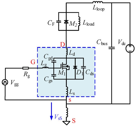
Figure 1.
Equivalent circuit model for the double-pulse test configuration.
2.1. Analysis of Turn-on Characteristics
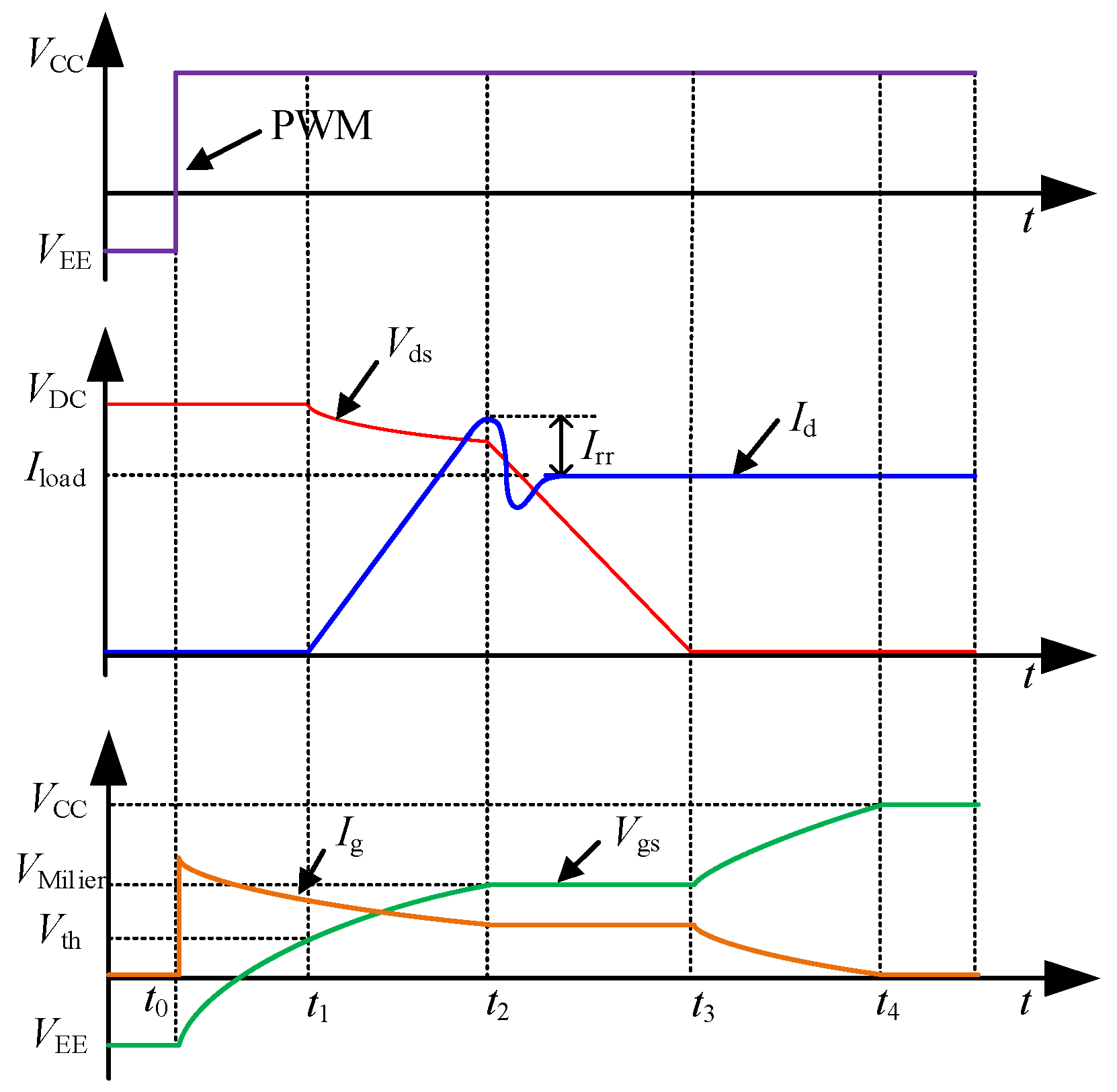
The characteristic curves of the turn-on process, depicted as Figure 2, are primarily divided into four stages:
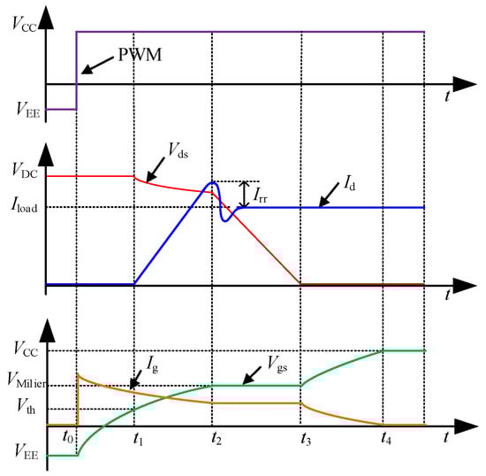
Figure 2.
The turn-on characteristics of SiC MOSFET.
Stage (t0~t1): When the gate charging is delayed, the gate-source voltage Vgs transitions from VEE (negative voltage) to VCC (positive voltage), with Ciss being charged via the gate drive resistor. During this stage, Vgs is less than the threshold voltage Vth, resulting in no change to Vds (drain-source voltage) and Id (drain current), which remain in a static state.
Stage (t1~t2): At t1, upon Vgs attaining the threshold voltage Vth, the gate current persists in charging the input capacitor Ciss, and the drain current Id incrementally ascends towards IL (load current). This rise can be subject to the influence of the reverse recovery current Ir from the anti-parallel diode. Id will continue to increase and reach the current spike Id_peak at t2. Id_peak can be expressed as follows:
Ir is positively related to the drain current change rate dId/dt:
where Qrr signifies the reverse recovery charge associated with the anti-parallel diode. The change rate of Id, denoted as dId/dt, can be approximated as follows:
According to (2) and (3), the relationship between Ir and Ig can be expressed as
It can be seen from Equation (4) that Ir is positively correlated with Ig. Therefore, reducing Ig can effectively reduce the drain current spike.
Stage (t2~t3): The reverse recovery charge is completely released, Id returns to IL and remains unchanged, and Vgs is clamped at the Miller voltage Vmiller. The gate-drain capacitor Cgd is charged with a constant gate current Ig, and the anti-parallel diode begins to block Vds. Vds gradually decreases to zero. Ig can be articulated by the following expression:
The rate of change for Vds is given by the expression:
Substituting Equation (6) into Equation (5), tdown, the duration of the Vds drop process, can be obtained as
Stage (t3~t4): The gate current continues to charge Cgs until the device is saturated. Vgs rises exponentially to the reference gate voltage VCC, Vds drops to a value close to zero, and Id is maintained at IL.
2.2. Analysis of Turn-off Characteristics
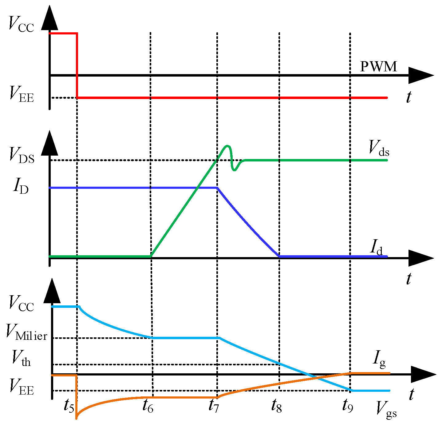
The characteristic curves of the turn-off process, depicted in Figure 3, are primarily divided into four stages:
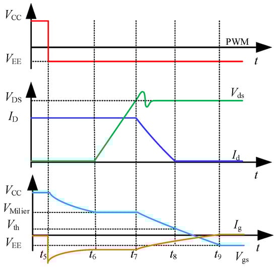
Figure 3.
The turn-off characteristics of SiC MOSFET.
Stage (t5~t6): The drive voltage transitions from VCC to VEE, and Ciss starts to discharge through the gate resistance Rg and source resistance Ls. Id and Vds remain unchanged. At t6, Vgs drops to the Miller voltage VMiller.
Stage (t6~t7): Vds gradually increases, but Id remains unchanged.
Stage (t7~t8): As Vgs descends to the threshold voltage, Id diminishes swiftly, thereby generating an induced voltage across the circuit’s parasitic inductance. This induced voltage, when combined with the DC-bus voltage, results in a voltage spike, denoted as Vds_peak. The spike can be formulated as
where Lloop represents the total parasitic inductance of the whole double-pulse circuit. The change rate of Id is
According to (9), diminishing the gate current Ig serves as an effective approach to curtailing voltage overshoot during the voltage increase stage.
Stage (t8~t9): Vgs drops to the negative voltage VEE. The overvoltage will oscillate, attenuated until stable.
In light of the preceding analysis, during the ascent of Id in the turn-on stage, the surge in Id can be mitigated by extracting Ig. Likewise, during the increase in Vds in the turn-off stage, the excess in Vds can be curtailed by injecting Ig. To minimize switching losses, the original Ig should be restored in other phases of the switching process. This restoration can shorten the charging and discharging duration of Cgd within the Miller plateau, thus enhancing the switching rate. This study introduces an active gate current adjustment circuit that leverages the transient feedback of the change rates of Vgs, Id, and Vds for dynamic regulation.
3. Hardware Implementation of the Proposed AGD Circuit
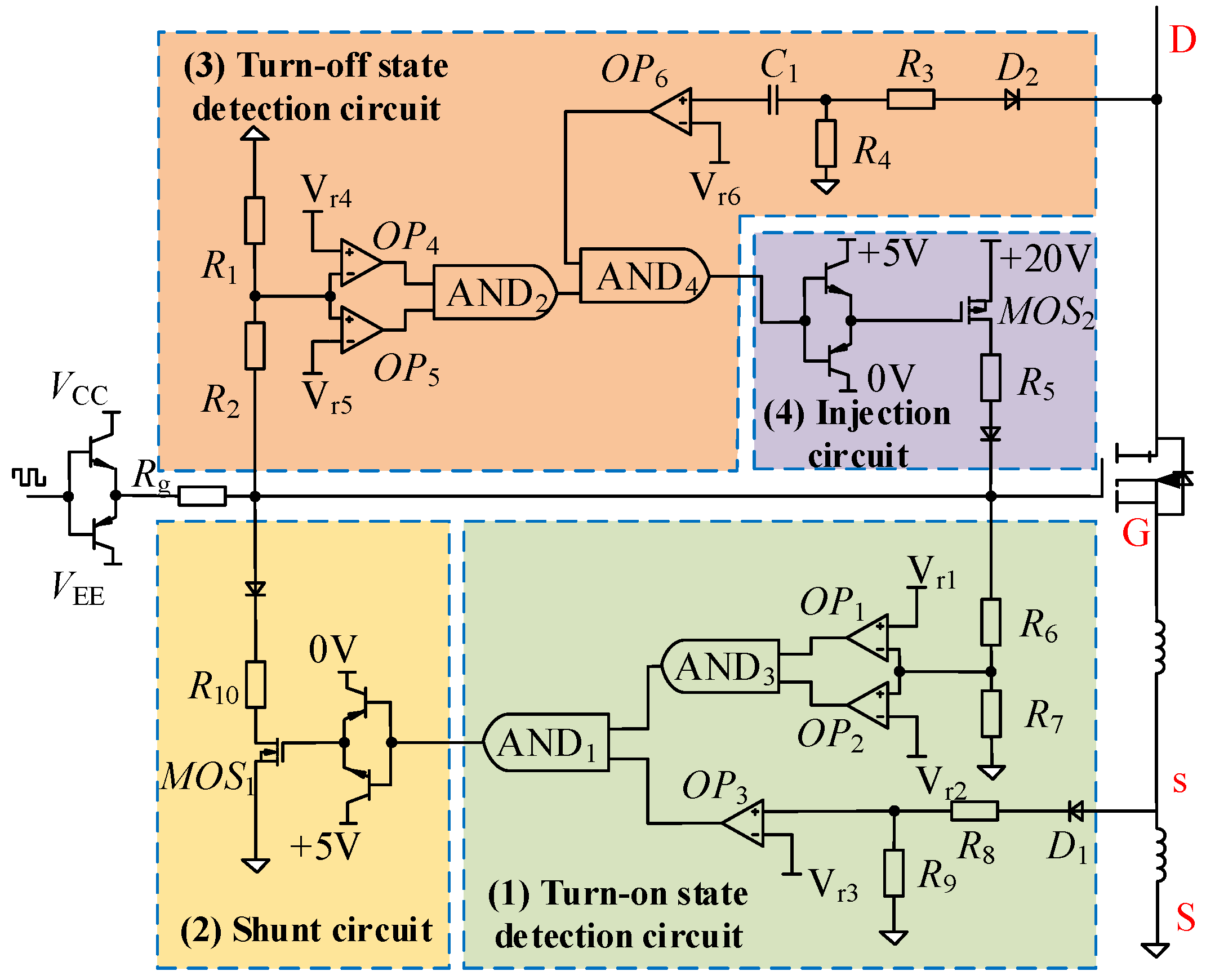
The proposed AGD circuit is shown in Figure 4. It is divided into four parts: (1) detection circuit of turn-on current rising state; (2) turn-off voltage rising state detection circuit; (3) current shunt circuit; and (4) current injection circuit. The specific implementation schemes of each circuit are as follows:
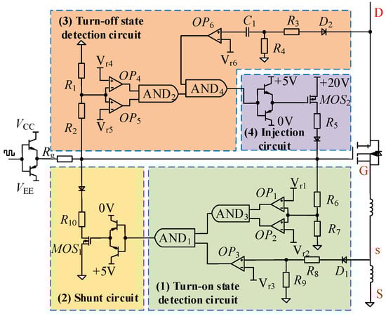
Figure 4.
Schematic of the proposed AGD.
(1) The detection circuit of the turn-on current rising state comprises a dId/dt detection circuit and a Vgs-on voltage detection circuit. The dId/dt detection circuit utilizes LsS, the parasitic inductance between the Kelvin source and the power source, which generates an induced voltage VsS due to the change in current, so the signal of dId/dt is converted into a voltage signal for detection. To detect the voltage signal during the current rising stage in the turn-on process, a diode D1 is employed to filter out spurious signals that may arise from the descent of the current during the turn-off stage. The induced voltage of LsS is detected when the SiC MOSFET is turned on, and is compared with the reference voltage Vr3 to generate a corresponding logic signal. The value of Vr3 is defined by the following equation:
The Vgs-on voltage detection circuit, with voltage dividing resistors (R6 and R7), comparators (OP1 and OP2) and AND gate (AND3), eliminates the interference from the current rising stage and Id oscillation after device turn-on. By detecting whether Vgs is within the interval [Vth, Vmiller] and using the logic signal from the dId/dt detection circuit, the phase of current increase during the turn-on process is accurately identified. The values of comparison voltages Vr1 and Vr2 are defined by the following equations, respectively.
(2) Voltage rising state detection circuit for turn-off stage: It consists of two parts, dVds/dt detection circuit and Vgs-off detection circuit. The detection circuit of the dVds/dt utilizes a differential circuit to calculate the voltage change rate of Vds during the turn-off stage, then the dVds/dt is converted into a voltage signal. This signal is compared with the reference voltage Vr6 through a comparator. It should be noted that the diode D2 is employed to block the interference signals generated during the turn-on stage. Vr6 is defined by the following equation:
Similarly to the turn-on part, the Vgs-off voltage detection circuit, consisting of voltage dividing resistors (R3 and R4), comparators (OP4 and OP5) and an AND gate (AND2), is designed to eliminate interference caused by Vds oscillation after the device is turned on. By detecting whether Vgs is within the interval [Vr4, Vr5] and cooperating with the logic output signal from the dVds/dt detection circuit, the phase of voltage increase during the turn-off process is accurately identified. The values of the comparison voltages Vr4 and Vr5 are determined by the following equations, respectively.
(3) Extraction circuit: It includes a push–pull amplifier circuit, MOS1, diode and resistor. The detection signal, generated by the current rising state detection circuit, is amplified by the push–pull circuit and drives the MOS1 to conduct. A portion of the gate current flows out through MOS1 and R10.
(4) Injection circuit: The structure is similar to that of the shunt circuit. The detection signal, generated by the turn-off voltage rising state detection circuit, drives the MOS2 to conduct through the push–pull circuit. Reversed gate current is injected into the gate, reducing the discharge current during the turn-off process.
4. Active Drive Control Process
4.1. Turn-on Process Control
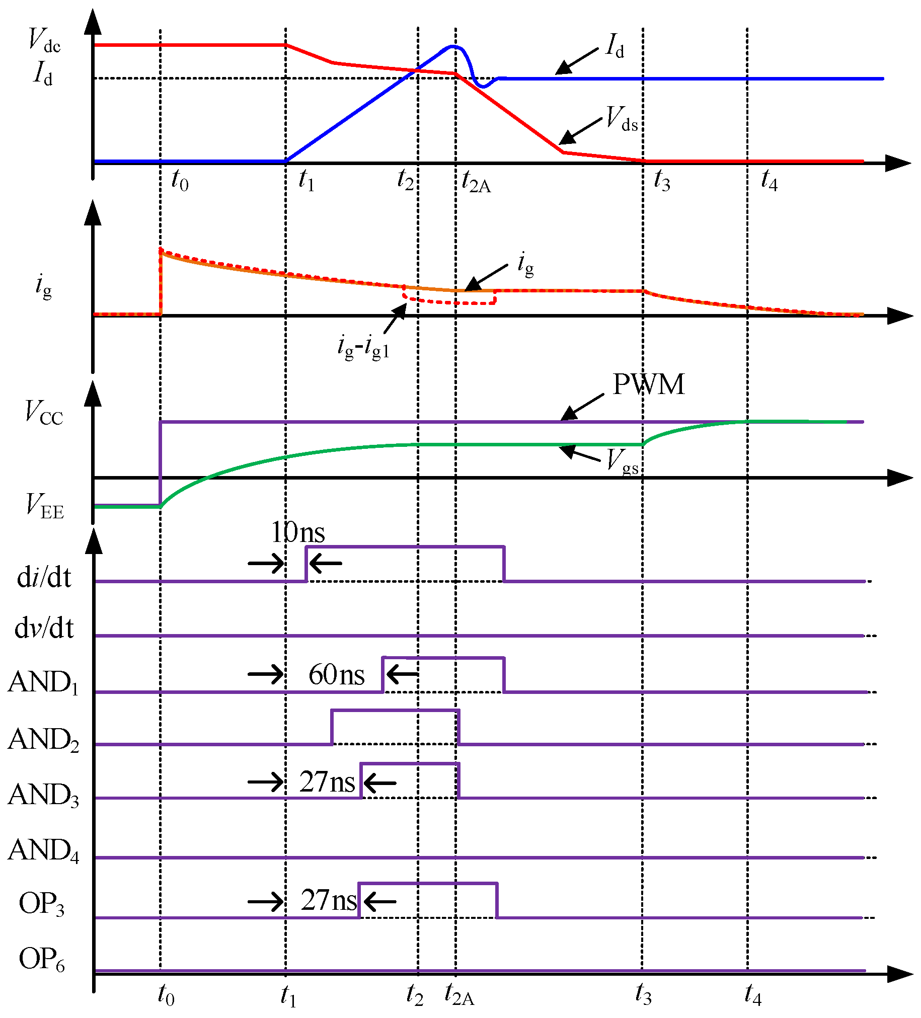
As the SiC MOSFET is turned on, Vgs, Id, Vds and other signal waveforms of each detection circuit are as shown in Figure 5. The control process is categorized into four stages.
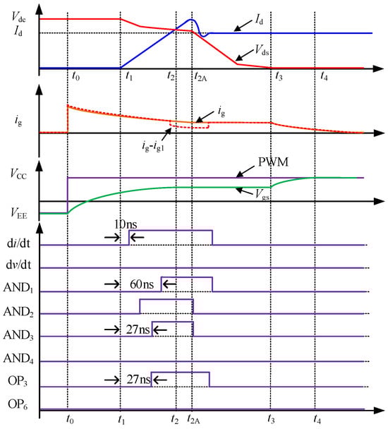
Figure 5.
The turn-on characteristics of AGD.
(1) During the delay stage (t0–t1), the external drive signal transitions from VEE to VCC, and Vgs gradually rises. At this stage, Vgs does not reach the lowest set voltage Vr2, so the AND3 outputs the low-level voltage. Both the dId/dt detection circuit and dVds/dt detection circuit have no induction signal output.
(2) During the current rising stage (t1–t2), when Vgs satisfies the math condition (Vr2 < Vgs < Vr1), the AND3 outputs the high-level voltage. At the same time, the rapidly rising gate current generates an induced voltage on the auxiliary source inductor LsS. After voltage division, when the induced voltage VsS satisfies the following condition:
(3) During the current oscillation stage (t2–t3), several cycles of oscillation will occur, causing the dId/dt detection circuit OP3 to generate a high-level signal again. However, since Vgs is larger than Vmiller, AND3 outputs the low-level voltage and MOS1 is turned off at this moment, so the circuit of the current extraction is blocked. Meanwhile, the gate drive current returns to Ig.
(4) During the stage (t3–t4), when the SiC MOSFET is fully turned on, the induction signal of the dId/dt detection circuit outputs a low-level voltage, the control circuit does not work, and MOS1 remains in the turn-off state.
4.2. Turn-off Process Control
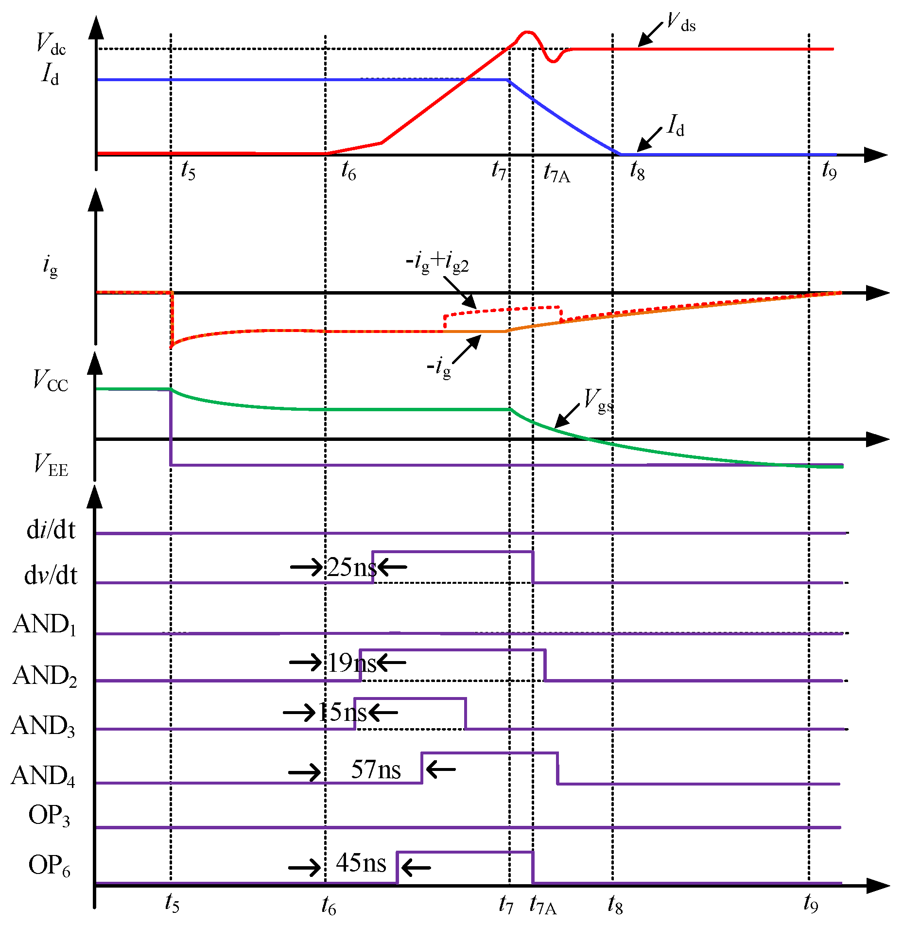
As the SiC MOSFET is turned off, Vgs, Id, Vds and other signal waveforms of each detection circuit are as shown in Figure 6. The control of the turn-off process mainly includes four stages.
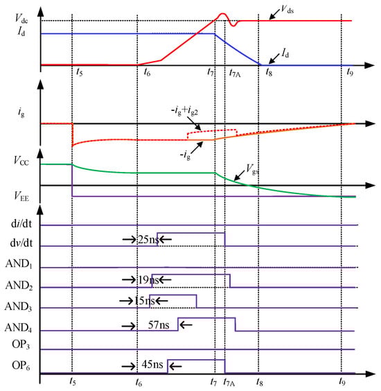
Figure 6.
The turn-off characteristics of AGD.
(1) During the turn-off delay stage (t5–t6), the external drive signal transitions from VEE to VCC, and Vgs gradually decreases. At this stage, Vgs is greater than Vr4, the maximum reference value set for the turn-off state detection circuit, and AND2 outputs the low-level voltage. The SiC device is in the turn-off delay stage, Both the dId/dt detection circuit and the dVds/dt detection circuit have no induction signal output.
(2) During the voltage rising stage (t6–t7), when the gate voltage satisfies the math condition (Vr5 < Vgs < Vr4), the AND2 of the turn-off detection circuit outputs high-level voltage. The drain-source voltage Vds rises rapidly, and the dVds/dt detection circuit generates an induced signal. The induced voltage signal is greater than the threshold voltage Vr6 after being divided by the resistor R3 and R4, and the comparator OP6 outputs high-level voltage. Then, the AND4 receives two high-level signals and outputs high-level voltage. After the push–pull amplifier circuit increases the current, the MOS2 is controlled to be turned on, the current injection circuit is turned on, and Ig2 is injected into the gate terminal. At the moment, the gate current is −Ig + Ig2, so the corresponding turn-off voltage overshoot is reduced.
(3) During the voltage oscillation stage (t7–t8), after the rising stage of Vds, Vds tends to stabilize after oscillating. The dVds/dt detection circuit will output a high-level signal again during the oscillation process. However, Vgs is less than Vr5 after voltage division. The AND4 outputs a low-level voltage, and MOS2 is turned off in time. The current injection circuit is blocked, and the gate drive current returns to Ig.
(4) During the stage (t8–t9), when the device is fully turned off, Vds and Ig tend to have a constant value, and the output of each detection circuit is low-level voltage. At this time, the control circuit does not work, and MOS2 remains in the turn-off state.
5. Experimental Results and Analysis
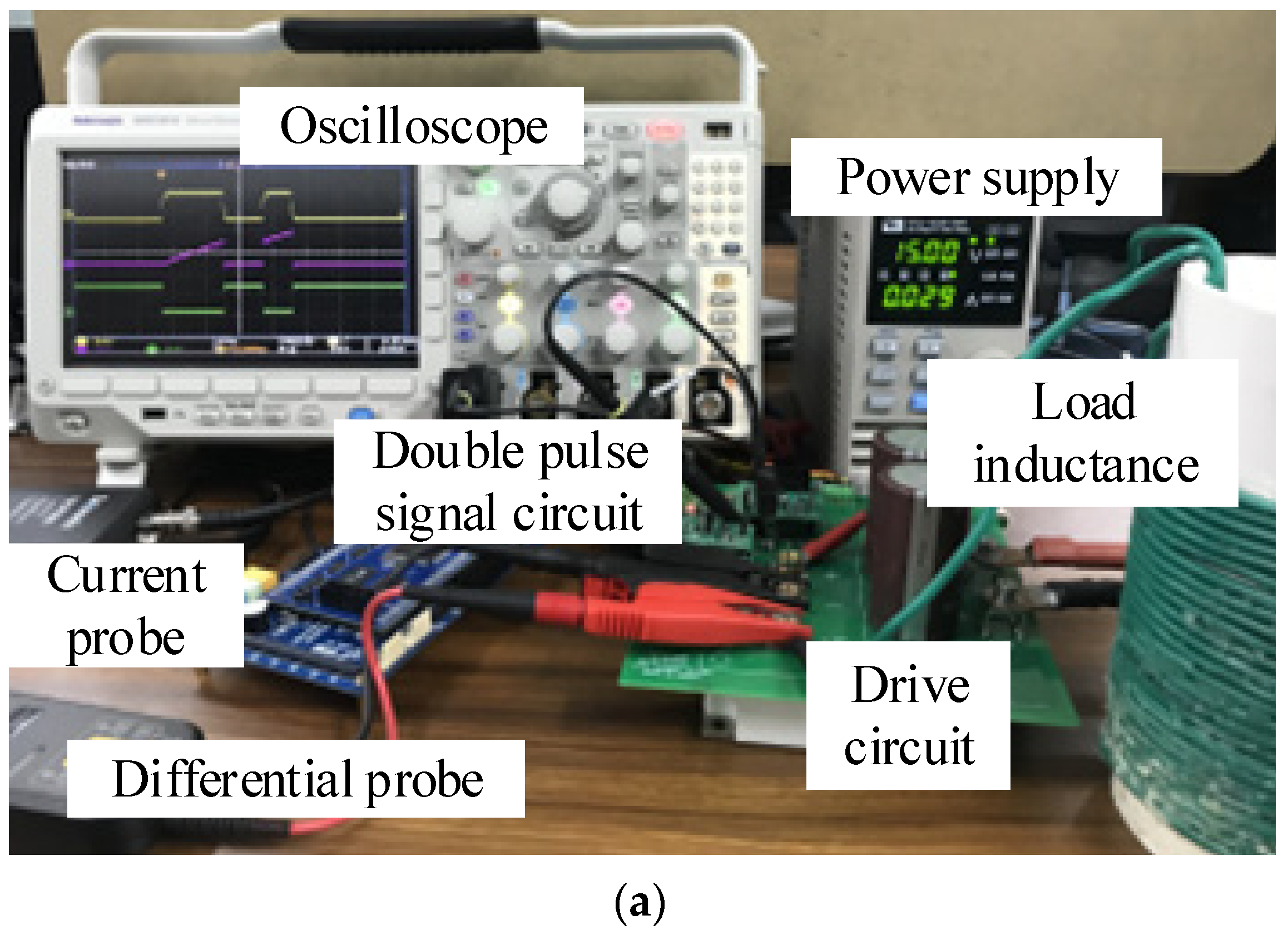
To substantiate the efficacy of the AGD circuit designed and proposed in this paper, an experimental setup of the double-pulse topology was established, as shown in Figure 7a. The SiC MOSFET module model was CAS300M12BM2, with its parameters provided in Table 1. The oscilloscope was a Tektronix MDO3024. A DSP28335 control board was utilized to produce the double-pulse signal, and the load inductance value was 48.5 μH. The proposed active gate drive circuit, as shown in Figure 7b, includes the detection and control circuit for the turn-on and turn-off processes, and the SiC MOSFET module is soldered under the circuit board.
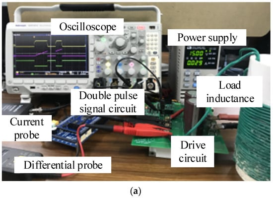
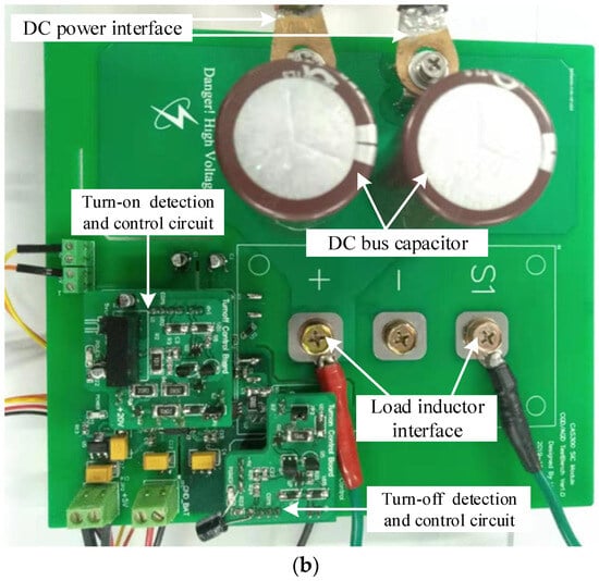
Figure 7.
The double-pulse testing experimental platform and circuit. (a) Experimental platform; (b) proposed active gate drive circuit.

Table 1.
The parameter values for the CAS300M12B2M module.
The models of the devices adopted in the AGD are listed in Table 2.
Table 2.
Models of devices used in the IC.
The experiment compared the current, voltage overshoot, oscillation and losses during the switching process for the proposed AGD and the conventional drive circuit (CGD) under different DC bus voltage levels, gate resistance and load current conditions. A total of nine groups of experimental operation conditions were established in this study, as shown in Table 3.
Table 3.
Experimental operation conditions.
5.1. Comparative Analysis of Different Gate Resistances
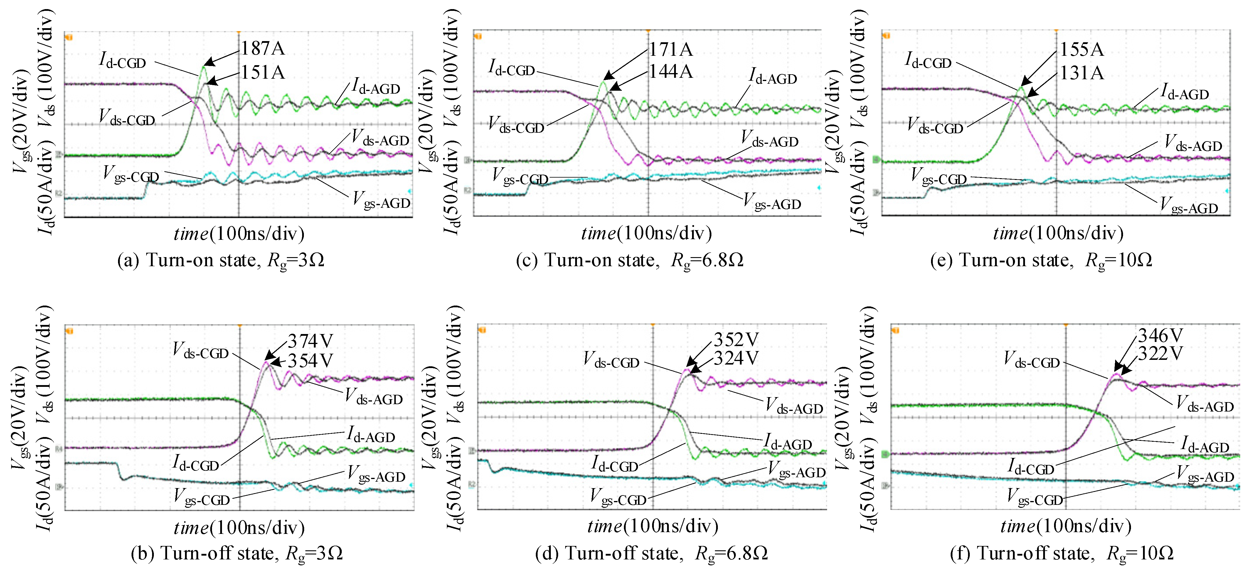
To validate the effectiveness of the proposed AGD circuit under different gate resistance conditions, the experimental conditions were set as follows: bus voltage 300 V, load current 110 A, and three different gate resistances of 3 Ω, 6.8 Ω and 10 Ω, respectively. Under the same operating conditions, the experimental waveforms of Id, Vds and Vgs under the proposed AGD circuit and under the CGD are as shown in Figure 8.
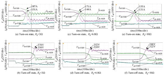
Figure 8.
Experimental waveforms of AGD and CGD under different values of Rg.
Figure 8a~f demonstrate that the proposed AGD has a significant suppression effect on overshoot and oscillation under different gate resistances. Among them, when the gate resistance is 3 Ω, the peak of Id decreases from 187 A to 151 A. When the SiC MOSFET is turned off, the peak of Vds decreases from 374 V to 354 V. When Rg is set as 6.8 Ω and 10 Ω, the current overshoot decreases by 27 A (44.3%) and 24 A (53.3%), respectively. The voltage overshoot decreases by 28 V (53.8%) and 24 V (52.1%), respectively. Meanwhile, the current and voltage of AGD can be quickly restored to steady state, with a smaller oscillation amplitude and shorter oscillation time.
5.2. Comparative Analysis of Different Voltage Levels
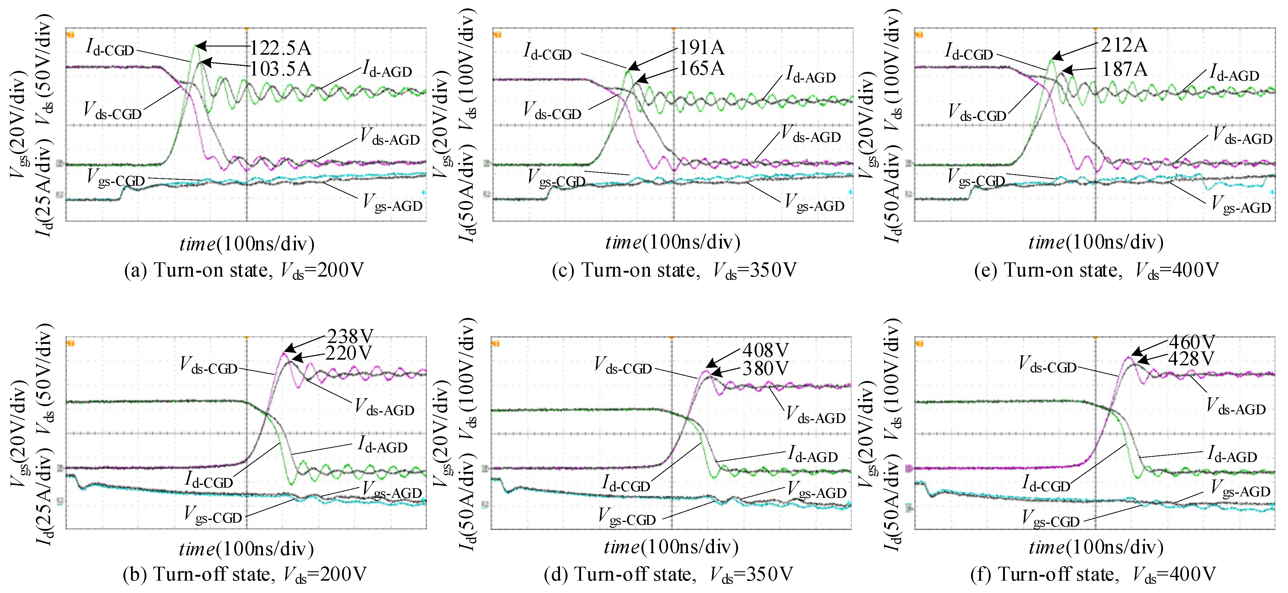
To verify that the designed active drive circuit has superiority at different voltage levels, the gate resistance was set to 6.8 Ω, the DC-bus voltage levels were set to 200 V, 300 V, 350 V, and 400 V, and the corresponding load currents were 74 A, 110 A, 129 A, and 147 A, respectively. The experimental results for AGD and CGD are shown in Figure 9a~f.
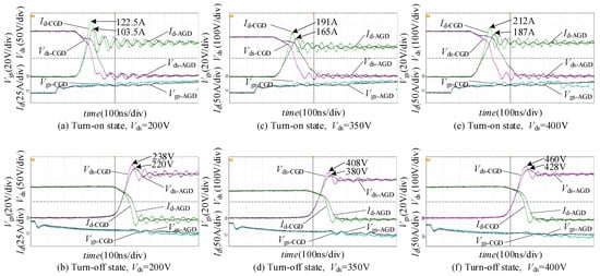
Figure 9.
Turn-on and turn-off waveforms at different values of Vds.
Figure 9a~f and Figure 8c,d illustrate that under the four different voltage level conditions, in the turn-on process, compared to CGD, the current overshoot of AGD decreases by 19 A, 26 A, 26 A, and 25 A, respectively, with an average decrease of 40.4%. In the turn-off process, compared to CGD, the suppression effect on the current and voltage oscillation is obvious.
5.3. Comparative Analysis of Different Load Current
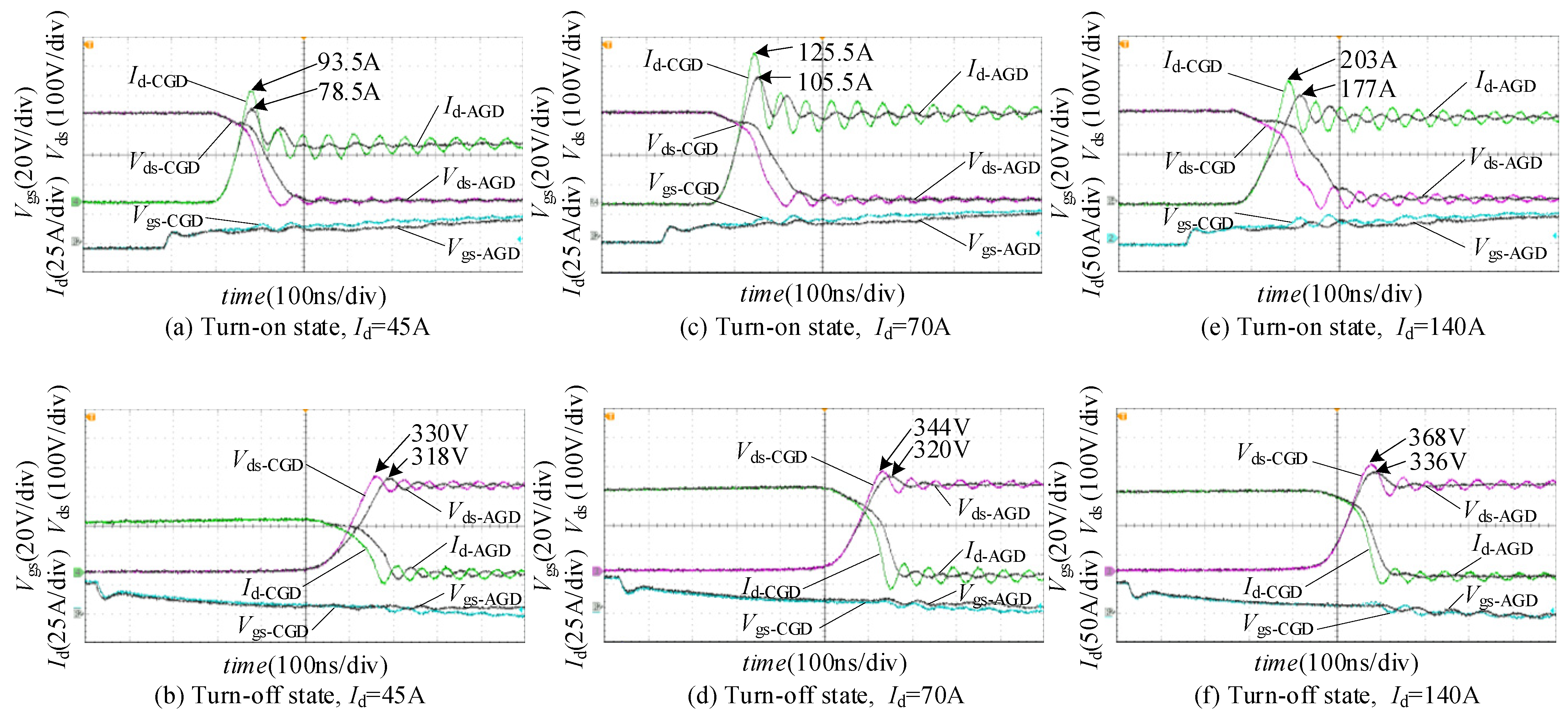
To verify that the proposed AGD circuit is effective under various load current conditions, the gate resistance and DC-bus voltage were set as 6.8 Ω and 300 V, respectively. Four different load currents of 45 A, 70 A, 110 A, and 140 A were obtained by changing the first pulse time. The results of the comparative experiment are depicted in Figure 10a~f.
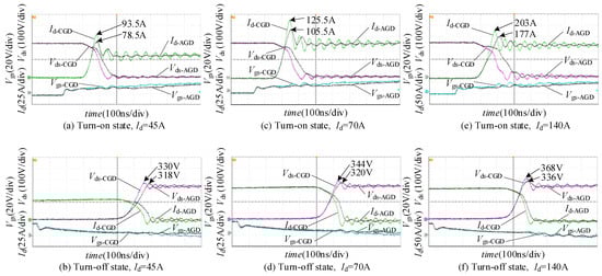
Figure 10.
Turn-on and turn-off waveforms at different values of Id.
Figure 10a~f and Figure 9c,d indicate that under the same gate resistance and bus voltage conditions, the current and voltage overshoot, oscillation amplitude, and oscillation time under the proposed AGD are significantly smaller than those under CGD. During the turn-on process, compared to CGD, the current overshoot of AGD decreases by 15 A, 20 A, 27 A and 26 A, respectively, with an average decrease of 39.1%. In the turn-off process, the voltage overshoot decreases by 12 V, 24 V, 28 V and 32 V, respectively, with an average decrease of 48.9%.
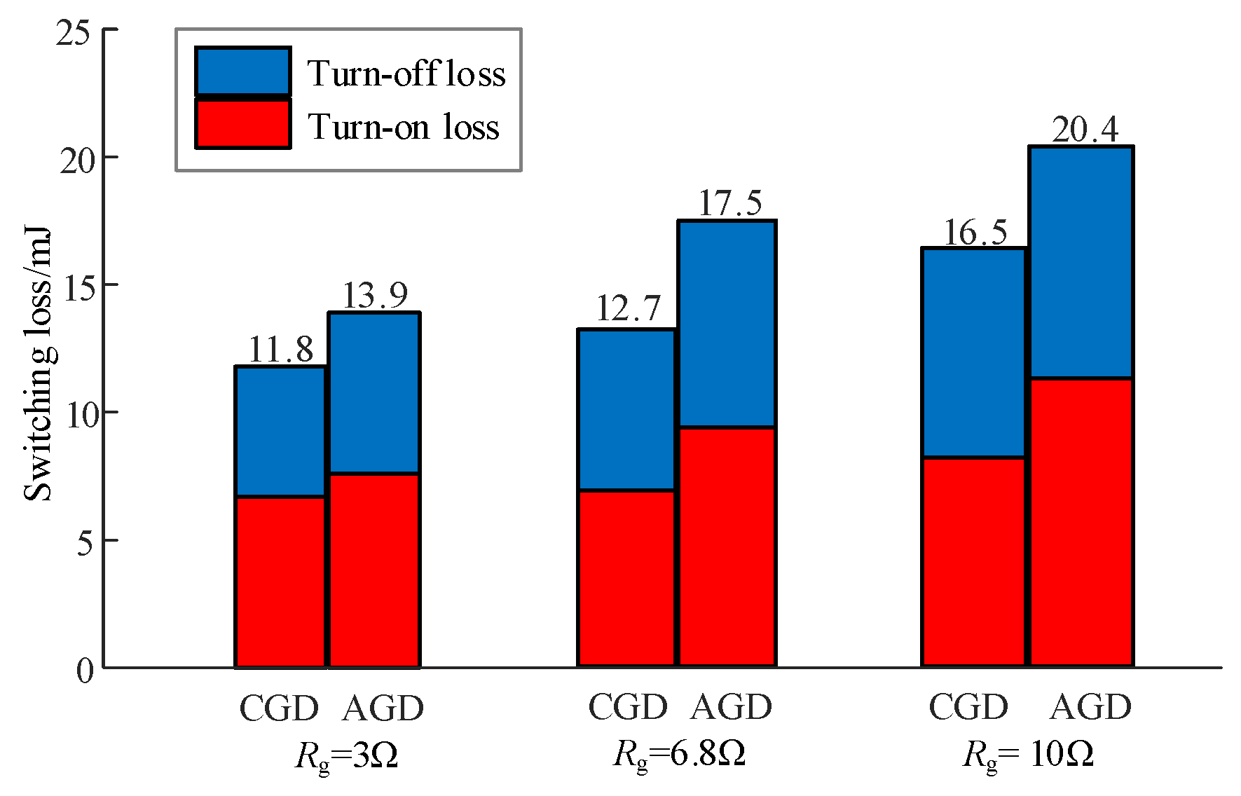
5.4. Comparative Analysis of Switching Loss under Different Conditions
The switching loss comparisons under different gate resistances are shown in Figure 11. Based on three group experiments under the same gate resistance condition, compared with CGD, the average switching loss of the proposed AGD only increased by 26.41%. Comparing Figure 8a with Figure 8e, it should be noted that the current suppression effect of the proposed AGD under Rg = 3 Ω, was the same as that of CGD under Rg = 10 Ω. However, the switching loss was 20.4 mJ, increasing by 46.76%.

Figure 11.
Switching loss at different gate resistances.
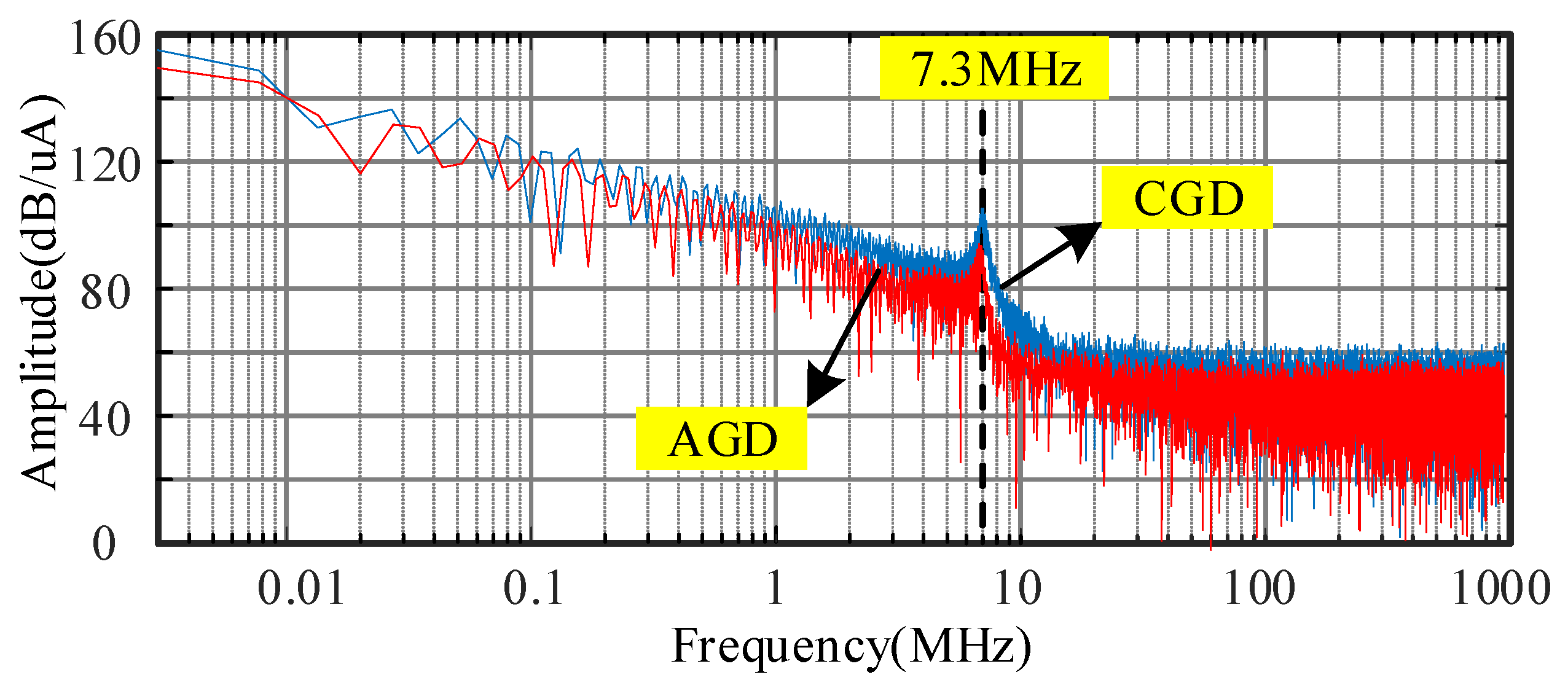
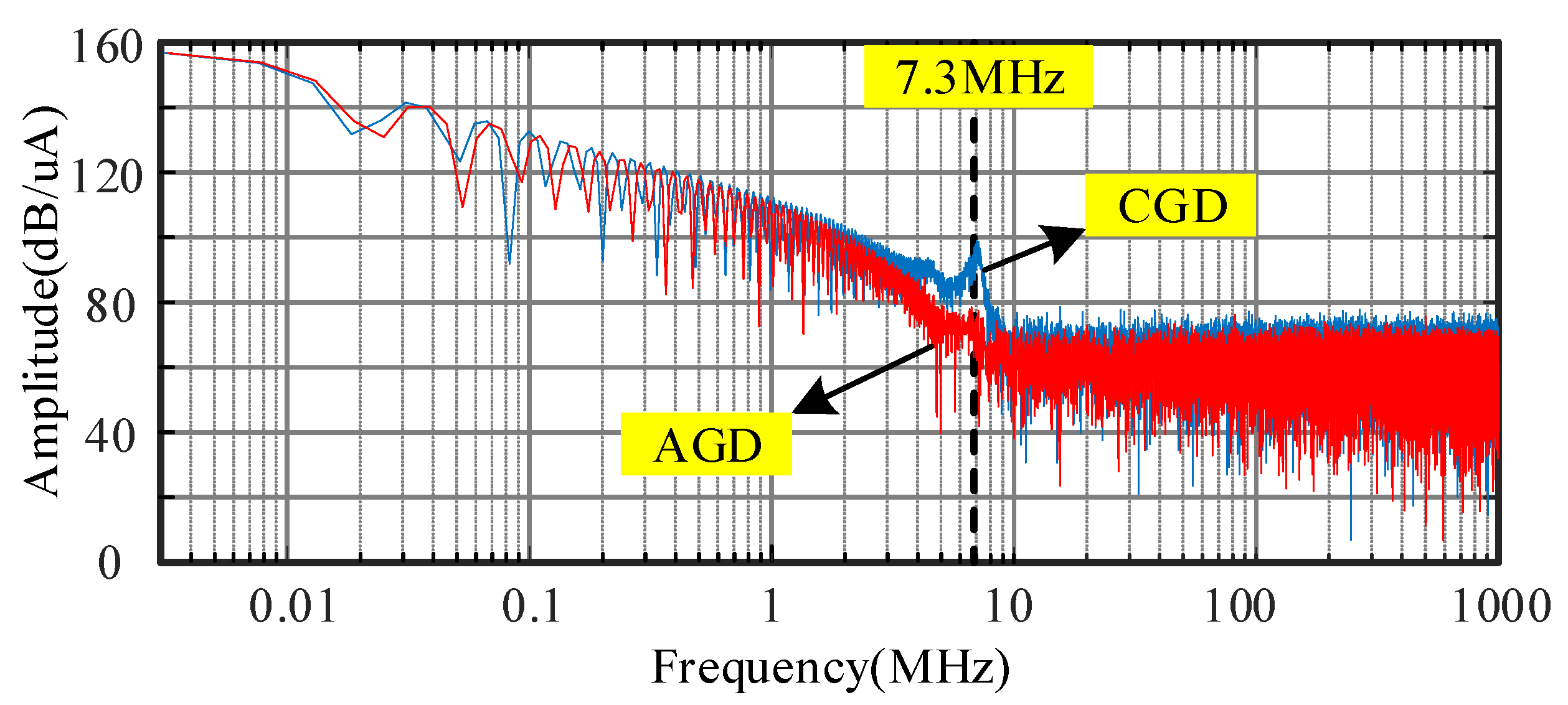
5.5. Comparative Analysis of EMI
By reducing the overshoot of Id and Vds during the turn-on and turn-off stages, the emission of high-frequency electromagnetic interference from the SiC MOSFET can be reduced. Under the conditions of Vds = 300 V, Id = 110 A, and Rg = 6.8 Ω, the spectrum analysis and comparison results for Id and Vds under the AGD and CGD circuits are as presented in Figure 12 and Figure 13, respectively. It is obvious that the current and voltage oscillations of CGD all generate spikes around 7.3 MHz, and the positions of the spikes are basically consistent with the oscillation frequency. However, the spectrum amplitude of AGD is significantly reduced, which verifies that the proposed AGD circuit can effectively mitigate electromagnetic interference in the SiC MOSFET switching process.
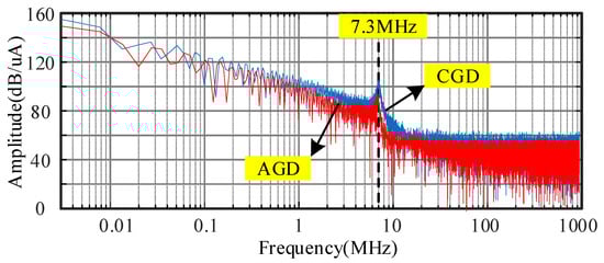
Figure 12.
Comparison of Id spectrum under different drivers.

Figure 13.
Comparison of Vds spectrum under different drivers.
6. Conclusions
Based on the switching transient state feedback, an active gate drive (AGD) circuit for SiC MOSFETs was proposed in this paper. Experimental results showed that the proposed AGD circuit can effectively reduce the overshoot and oscillations of the SiC MOSFET drain current and drain-source voltage. The following conclusions were formed:
- (1)
- This paper proposes a high-precision transient detection method. The gate voltage and change rate of the drain current together serve as the basis for determining the current rise stage during the turn-on process, and the gate voltage and change rate of the drain-source voltage together serve as the basis for determining the voltage-rising stage during the turn-off process.
- (2)
- This experiments in this paper only reduced the gate drive current during the current-rising stage, injected the gate current during the voltage-rising stage, and did not perform any operations during other stages of the switching process. Therefore, as the experimental results indicate, without affecting the switching speed, the overshoot and oscillation of the drain current and drain-source voltage can be effectively suppressed.
- (3)
- The AGD scheme proposed in this paper has a simple structure and strong universality, eliminating the need for a digital signal processor. The resistance of the current extraction circuit and current injection circuit and the threshold voltage can be adjusted to satisfy the requirements of the switching speed, switching loss, current and voltage overshoot.
Author Contributions
Conceptualization, C.X.; methodology, Y.M.; software, Y.M.; validation, C.X.; formal analysis, C.X.; investigation, Y.M.; writing—original draft preparation, Y.M.; writing—review and editing, C.X.; project administration, C.X.; funding acquisition, C.X. and Y.M. All authors have read and agreed to the published version of the manuscript.
Funding
This work is supported by the grant of Ji Hua Laboratory (No. X220271XE220), and the natural sciences funding project of Fujian Province (No. 2022J05109).
Data Availability Statement
The original contributions presented in the study are included in the article, further inquiries can be directed to the corresponding author.
Conflicts of Interest
The authors declare no conflict of interest.
References
- Zhao, S.; Zhao, X.; Dearien, A.; Wu, Y.; Zhao, Y.; Mantooth, H.A. An Intelligent Versatile Model-Based Trajectory-Optimized Active Gate Driver for Silicon Carbide Devices. IEEE J. Emerg. Sel. Top. Power Electron. 2020, 8, 429–441. [Google Scholar] [CrossRef]
- Karout, M.A.; Taha, M.; Fisher, C.A.; Deb, A.; Mawby, P.; Alatise, O. Impact of Diode Characteristics on 1.2 kV SiC MOSFET and Cascode JFET Efficiency: Body Diodes Vs SiC Schottky Barrier Diodes. In Proceedings of the 2023 IEEE Applied Power Electronics Conference and Exposition (APEC), Orlando, FL, USA, 19–23 March 2023; pp. 202–208. [Google Scholar]
- Dong, Z.; Song, Z.; Wang, W.; Liu, C. Improved Zero-Sequence Current Hysteresis Control-Based Space Vector Modulation for Open-End Winding PMSM Drives With Common DC Bus. IEEE Trans. Ind. Electron. 2023, 70, 10755–10760. [Google Scholar] [CrossRef]
- Woldegiorgis, D.; Wu, Y.; Wei, Y.; Mantooth, H.A. A High Efficiency and Low Cost ANPC Inverter Using Hybrid Si/SiC Switches. IEEE Open J. Ind. Appl. 2021, 2, 154–167. [Google Scholar] [CrossRef]
- Zhao, S.; Dearien, A.; Wu, Y.; Farnell, C.; Rashid, A.; Luo, F.; Alan, H. Adaptive Multi-Level Active Gate Drivers for SiC Power Devices. IEEE Trans. Power Electron. 2020, 35, 1882–1898. [Google Scholar] [CrossRef]
- Miryala, V.K.; Dhanasekaran, S.; Ganesan, P.; Hatua, K.; Bhattacharya, S. Active Gate Driving Technique for Series Connecting SiC MOSFETs in the Presence of Gate Pulse Delay Mismatch. IEEE Trans. Ind. Electron. 2022, 69, 12402–12413. [Google Scholar] [CrossRef]
- Yoon, H.; Seok, O. Design of a 1.2 kV SiC MOSFET with Buried Oxide for Improving Switching Characteristics. Electronics 2024, 13, 962. [Google Scholar] [CrossRef]
- Henn, J.; Lüdecke, C.; Laumen, M.; Beushausen, S.; Kalker, S.; Engelmann, G. Intelligent Gate Drivers for Future Power Converters. IEEE Trans. Power Electron. 2022, 37, 3484–3503. [Google Scholar] [CrossRef]
- Shao, T.; Zheng, T.; Li, H.; Liu, J.; Li, Z.; Huang, B.; Qiu, Z. The Active Gate Drive Based on Negative Feedback Mechanism for Fast Switching and Crosstalk Suppression of SiC Devices. IEEE Trans. Power Electron. 2022, 37, 6739–6754. [Google Scholar] [CrossRef]
- Liu, P.; Li, H.; Miao, Y.; Chen, C.; Chen, Z.; Meng, J. Low Overshoot and Low Loss Active Gate Driver for SiC MOSFET based on Driving Current Dynamic Regulation. Proc. CSEE 2020, 31, 142–152. [Google Scholar]
- Camacho, A.P.; Sala, V.; Ghorbani, H.; Martinez, J.L.R. A Novel Active Gate Driver for Improving SiC MOSFET Switching Trajectory. IEEE Trans. Ind. Electron. 2017, 64, 9032–9042. [Google Scholar] [CrossRef]
- Yamaguchi, K.; Katsura, K.; Yamada, T.; Sato, Y. Comprehensive Evaluation of Gate Boost Driver for SiC-MOSFETs. In Proceedings of the 2016 IEEE Energy Conversion Congress and Exposition (ECCE), Milwaukee, WI, USA, 18–22 September 2016; pp. 1–8. [Google Scholar]
- Yang, Y.; Wen, Y.; Gao, Y. A Novel Active Gate Driver for Improving Switching Performance of High-Power SiC MOSFET Modules. IEEE Trans. Power Electron. 2019, 34, 7775–7787. [Google Scholar] [CrossRef]
- Wen, Y.; Yang, Y.; Gao, Y. Active Gate Driver for Improving Current Sharing Performance of Paralleled High-power SiC MOSFET Modules. IEEE Trans. Power Electron. 2021, 36, 1491–1505. [Google Scholar] [CrossRef]
- Dymond, H.C.P.; Liu, D.; Wang, J. Multi-level Active Gate Driver for SiC MOSFETs. In Proceedings of the 2017 IEEE Energy Conversion Congress and Exposition (ECCE), Cincinnati, OH, USA, 1–5 October 2017; pp. 5107–5112. [Google Scholar]
- Sukhatme, Y.; Miryala, V.K.; Ganesan, P.; Hatua, K. Digitally Controlled Gate Current Source-Based Active Gate Driver for Silicon Carbide MOSFETs. IEEE Trans. Ind. Electron. 2020, 67, 10121–10133. [Google Scholar] [CrossRef]
- Li, X.; Lu, Y.; Ni, X.; Wang, S.; Zhang, Y.; Tang, X. An Active Gate Driver for Improving Switching Performance of SiC MOSFET. Proc. CSEE 2020, 40, 5760–5769. [Google Scholar]


Disclaimer/Publisher’s Note: The statements, opinions and data contained in all publications are solely those of the individual author(s) and contributor(s) and not of MDPI and/or the editor(s). MDPI and/or the editor(s) disclaim responsibility for any injury to people or property resulting from any ideas, methods, instructions or products referred to in the content. |
© 2024 by the authors. Licensee MDPI, Basel, Switzerland. This article is an open access article distributed under the terms and conditions of the Creative Commons Attribution (CC BY) license (https://creativecommons.org/licenses/by/4.0/).