Abstract
The influence of Bi doping on the structural and thermoelectric properties of Cu2Se is presented in this work. Cu2−xBixSe (x = 0.00, 0.004, 0.008, 0.012) samples were prepared using conventional solid-state reaction techniques. According to room temperature XRD results, Cu2−xBixSe samples have a monoclinic crystal structure. Doping Bi to the Cu site acts as a donor, lowering the hole concentration, except for the sample with x = 0.004. The resistivity of the Cu2−xBixSe sample increases with an increase in Bi content. Seebeck coefficient data confirm that the holes are the charge carriers in Cu2−xBixSe samples. At 700 K, the Cu1.988Bi0.012Se sample has the highest power factor of 1474 μWm−1K−2, showing great potential in developing high-performance Cu2Se based thermoelectric materials.
1. Introduction
The increasing demand for energy caused by the expanding global population places extreme strain on the available energy supplies. Due to the finite supply of fossil fuels and their detrimental effects on the environment, the research community is exploring sustainable energy harvesting techniques to satisfy the world's current energy needs. The globe paradoxically faces a shortage of renewable energy resources on the one hand. On the other side, a tremendous quantity of heat is produced by our industrial operations, car exhaust, and building heating systems, which is wasted in the environment. Such waste heat may be converted into energy (electricity) to assist us in satisfying our energy needs while also preserving the environment [1]. Thermoelectric materials can directly convert temperature differences to electricity, making them a viable solution to energy problems and pollution [2]. Thermoelectric devices are solid-state devices with no moving parts, and they have the benefits of cheap maintenance, high dependability, and exceptional scalability. The thermoelectric (TE) devices emit no greenhouse gases, making them environmentally beneficial. The scientific world has been attracted to thermoelectric materials for decades due to all their unique properties. Nevertheless, TE devices are insufficient when compared to their traditional counterparts due to their low efficiency. For the scientific community, creating TE materials with greater efficiency has remained a challenging part [1]. In the mid-1990s, theoretical predictions suggested that nanostructure engineering might considerably improve thermoelectric efficiency, prompting experimental efforts to demonstrate proof-of-principle and high-efficiency materials [3]. Thermoelectric materials convert heat into electricity through Seebeck effect. Utilizing the Peltier effect, they act as cooling devices when they are used in a reverse manner.
The power factor, , is used to evaluate the efficiency of thermoelectric materials where σ and S are electrical conductivity, and the Seebeck coefficient respectively [4]. Because of their potential for good thermoelectric performance, many materials have been investigated. Bi-Te alloys [5,6], Half-Heusler compounds [7,8], PbTe [9,10], SnSe [11,12], and skutterudites [13] are a few of the most well-known. Cu2Se-based compounds have recently received much attention because of their low thermal conductivity, toxicity, earth abundance, and cheapness [14]. Recent years have seen the development of a number of novel methods, including Phonon-Glass-Electron-Crystal (PGEC) paradigm, the use of band resonant states to enhance the density of states, formation of bulk nano-composite structures, increasing the band degeneracy by prompting band convergence by varying the composition or temperature, using ultrafast solidification techniques, seeking material with extreme anharmonicity of lattice vibration and even Phonon-Liquid-Electron Crystal (PLEC) concepts have all been proposed to enhance the efficiency of thermoelectric materials. It seems to work well in super-ionic compounds such as Cu2−xX (X = S, Se, Te). Although having a straightforward chemical formula, copper chalcogenides have a very complicated crystal structure. Heyding was the first to report on the structure and phase diagram of Cu2Se; various groups thereafter conducted thorough structural investigations [15].
Cu2Se has two distinct crystal structures: the α-phase at low temperatures and the β-phase at high temperatures. Doping is one of the most significant methods for improving a material's thermoelectric characteristics. Several dopants have been suggested to improve the chemical stability, the Seebeck coefficient, or the electrical conductivity of copper selenide to improve its thermoelectric performance [14]. Many researches were done on doping different dopants like Mg [16], Na [17], Ni [14], Te [1], K [18], etc in Cu2Se system. The power factor of Cu1.99Mg0.01Se ~ 1200 μWm−1K−2 [16], Cu1.96Na0.04Se ~ 900 μWm−1K−2 [17], Cu2Se ~ 1100 μWm−1K−2 [2], Cu1.99K0.01Se~900 μWm−1K−2 [18] at 700 K. Heavy-element dopants have piqued our interest, implying that doping heavy-element is a viable technique to increase the complexity system [2]. Recently Liao et al. [19] studied Bi-doped α-Cu2Se near room temperature, and Lisha Xue et al. studied the impact of Bi doping on the thermoelectric characteristics of Cu2Se materials [2]. Bismuth is doped into Cu2Se to enhance its electrical property.
The fabrication of pure copper selenide and doped material has been proposed using various techniques, such as high-temperature, high-pressure technology, mechanical alloying, melting followed by spark plasma sintering, and the conventional solid-state sintering method [1,2,14,19,20]. S. Mangavati et al. used a solid-state reaction technique to prepare Te-doped Cu2Se and obtained a power factor of ~ 800 μWm−1K−2 at 350 K [1]. Zhiming Geng et al. used the solid-state reaction technique to prepare Cu2Se and obtained a power factor of ~ 780 μWm−1K−2 at 350K [20]. The present work uses the solid-state reaction technique to synthesize Cu2−xBixSe (x = 0.00, 0.004, 0.008, 0.012) samples. The effects of Bi doping on electrical, structural, and other thermoelectric properties of Cu2Se are investigated.
2. Experiment Details
Material Synthesis
Polycrystalline Cu2Se and Bi-doped Cu2−xBixSe samples were produced using a standard solid-state reaction approach. Cu (99.7%, Loba Chemie, Mumbai, India), Se (99%, Molychem, Mumbai, India), and Bi (99%, Molychem, Mumbai, India) powders were taken and mixed using a mortar pestle according to stoichiometric ratios. The powders were compressed into rectangular pellets using a hydraulic press with a 5 MPa pressure. These pellets were sealed in quartz tubes under a high vacuum (10−6 mBar). The sealed quartz tube was placed in furnace at 973 K for 72 h. Later, the furnace was allowed to cool to room temperature naturally. Further, the obtained pellets were ground, pelletized, vacuum sealed, and sintered at 473 K for 48 h. Two-step sintering was performed to obtain more homogeneous compounds. Figure 1 shows the schematic representing the synthesis process of Cu2−xBixSe samples.
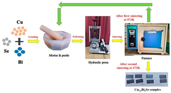
Figure 1.
Schematic representing the synthesis process of Cu2−xBixSe samples.
To examine the crystallographic details of the prepared samples, X-ray diffraction (Rigaku miniflex 600) using wavelength of Cu Kα (λ = 1.5406 Å) studies at room temperature were performed. Rietveld refinement technique with the Fullproof program was used to acquire crystallographic information. To study the morphology of the compound Scanning Electron microscope (SEM) (JEOL, JSM-7610FPlus) micrographs were taken. Energy Dispersive X-ray Spectroscopy (EDS) analysis was carried out to study the chemical composition of the prepared sample. The room-temperature Hall effect measurement was carried out using Ecopia HMS—5500 system to determine the carrier concentration and mobility using a field strength of 0.5 T. High-temperature electrical resistivity and thermopower are measured simultaneously using the Linseis LSR—3 system.
3. Results and Discussion
3.1. X-ray Diffraction (XRD) Analysis
The powder X-ray diffraction studies of the Cu2−xBixSe (x = 0,0.004,0.008,0.012) samples show that all the materials are polycrystalline in nature. The structure of the undoped sample is found to be monoclinic with the space group of Cm. Also, all the doped samples exhibited monoclinic structure with the space group P21/c [1]. The Rietveld refinement technique with the Fullprof program was used to acquire the crystallographic information of pure and Bi-doped Cu2Se samples. The XRD pattern of the Rietveld refined graph is represented in Figure 2. Vertical lines are used to represent all permitted peaks, and blue lines are used to depict the difference between the observed and fitted patterns for each peak. For all the four samples the major peak is located at θ = 44º. From the Rietveld refinement technique the values of lattice parameters, χ2 and other goodness of fitting parameters (Rp, Rwp, Rexp) are estimated. Table 1 lists the values of several parameters of Cu2−xBixSe samples calculated from the refinement. Here, a, b and c are the lattice parameters. Since the Cu2−xBixSe samples are monoclinic a ≠ b ≠ c, and α = β = 90°, γ = 101°. The obtained χ2 value of Cu2Se is 1.995, Cu1.996Bi0.004Se is 2.289, Cu1.992Bi0.008Se is 1.538, Cu1.988Bi0.012Se is 1.531.
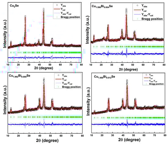
Figure 2.
Rietveld refinement X-ray plots of Cu2−xBixSe samples.

Table 1.
Rietveld refined crystallographic parameters and fitting parameters for Cu2−xBixSe samples.
XRD data was further analyzed to understand the effect of crystallite size and strain on the physical characteristics of the examined samples. It is widely known that the strain and crystallite size within the unit cell affects the XRD peak broadening. To distinguish the contribution of both effects multiple approaches, including Scherrer, modified Scherrer, and size strain plot (SSP), were used to identify the contribution of both effects, which are described in the following sections.
3.1.1. Scherrer Method
The peak broadening with crystallite size and lattice strain resulting from dislocation may be assessed using the straightforward and effective XRD peak profile analysis. Based on the Scherrer equation, the average crystallite size was determined from the XRD peak [21],
where β is full width at half maximum, D is crystallite size, θ is diffraction angle, K is shape factor (here the value of K is taken as 0.9), λ = 1.5406 Å. The crystallite size varies from 16 nm to 36 nm, tabulated in Table 2. Dislocation density (δ), defined as the length of dislocation per unit volume of crystal, represents the number of flaws in the sample. The equation for calculating dislocation density is as follows [21]:
Table 2.
Crystallite size, dislocation density, and strain of the sample calculated from Scherrer, modified Scherrer method, and size strain plot.
the strain (ε) is estimated using the following equation:
3.1.2. Modified Scherrer Method
The modified Scherrer formula is based on the concept that applying the least square approach reduces the source of error, and one can obtain the average values of D through all the peaks. The equation used in the modified Scherrer method is [22],
hence the plot of lnβ versus ln(1/cosθ) for all or part of the specified peaks can be linear, as presented in Figure 3. The value of ln(Kλ/D) can be calculated from the intercept after establishing the best linear plot. The value of crystallite size is calculated using the equation given below [23],
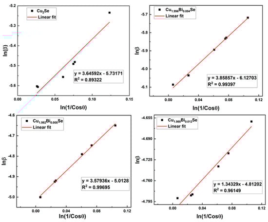
Figure 3.
Modified Scherrer plots of Cu2−xBixSesamples.
In modified Scherrer method the crystallite size varies between 17–64 nm and the dislocation density vary from 0.5 to 4 × 10¹⁵ lines/m2.
3.1.3. Size-Strain Plot (SSP)
The role of strain for broadening is excluded in Scherrer and modified Scherrer methods. As a result, SSP is used to compute the crystallite size, which considers both size and strain contributions. One of the advantages of this strategy is that data from the high-angle reflections are given less weightage, where precision is typically low [21]. The strain profile is expected to be explained by the Gaussian function and crystallite size profile by the Lorentzian function and is given by [21],
and a graph of versus is plotted as shown in Figure 4. Slope and intercept were obtained from this graph which was further used to calculate crystallite size and strain respectively. The slope and intercept were obtained from this graph. The crystallite size is evaluated by,
the Strain is estimated by the following Equation [21],
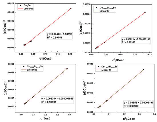
Figure 4.
Size-Strain plots of Cu2−xBixSe samples.
In SSP method, the crystallite size varies from 17–32 nm. Figure 4 displays a better fit, where all the data points are in a straight line. The conclusion drawn from the various approaches is that the crystallite size and micro-strain measurements acquired using the SSP are more accurate than those made using the other two methods for the materials used in the current study.
3.2. SEM and EDS Analysis
Figure 5A shows the SEM images of Cu2−xBixSe (x = 0.00, 0.004, 0.008, 0.012) samples. All the samples exhibit polycrystalline nature with randomly oriented grains. Due to the low dopant concentration, all samples have a similar morphology. Since sintering was performed at low temperatures, the examined samples do not exhibit clear grain development. Less porosity is observed in all the examined samples implying that the synthesized samples are dense, and grains are well connected. A high grain density can increase the number of grain boundaries in the material, which can act as a barrier to the movement of charge carriers (electrons or holes) and increase their scattering. This, in turn, can increase the Seebeck coefficient of the material. The presence of small grains between larger grains indicates grain size non-uniformity, which could scatter phonons and lower lattice heat conductivity [1].
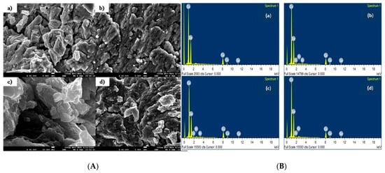
Figure 5.
(A) SEM images of (a) Cu2Se, (b) Cu1.996Bi0.004Se, (c) Cu1.992Bi0.008Se, (d) Cu1.988Bi0.012Se samples. (B) EDS spectrum of (a) Cu2Se, (b) Cu1.996Bi0.004Se, (c) Cu1.992Bi0.008Se, (d) Cu1.988Bi0.012Se samples.
The chemical composition of the prepared sample is estimated using Energy Dispersive X-ray Spectroscopy (EDS). EDS spectra of Cu2−xBixSe are shown in Figure 5B, and corresponding results are tabulated in Table 3. EDS data reveals that the chemical composition of prepared samples is close to the nominal composition within experimental limits. Figure 6a–d shows the elemental composition of Cu2−xBixSe samples.
Table 3.
EDS results of Cu2−xBixSe (x = 0.00, 0.004, 0.008, 0.012) samples.
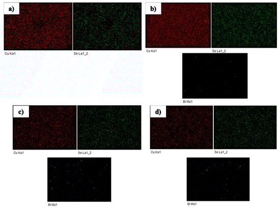
Figure 6.
EDS map of (a) Cu2Se, (b) Cu1.996Bi0.004Se, (c) Cu1.992Bi0.008Se, (d) Cu1.988Bi0.012Se.
3.3. Electrical and Thermelectric Transport Properties
3.3.1. Hall Measurement
The room temperature mobility and carrier concentration of all the samples is given in Table 4. The positive sign of the carrier concentration indicates that pristine and Bi-doped samples are p-type semiconductors. The plot of carrier concentration and mobility versus Bi content is shown in Figure 7. It is observed that carrier concentration and mobility follow the opposite trend except for x = 0.012. The carrier concentration of the pristine Cu2Se sample is 18 × 1020 cm−3. Bi acts as an electron donor [16]. It reduces the carrier concentration up to x = 0.008. After that, it significantly increases. This is due to the incorporation of trivalent Bismuth compensating for the Cu deficiency. The solubility of Bi is low in the Cu-Se matrix; hence after x = 0.008, it can regenerate the Cu deficiency, thereby enhancing the carrier concentration for x = 0.012 [19].
Table 4.
Carrier concentration and mobility of Cu2−xBixSe samples.
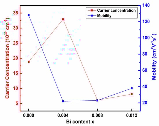
Figure 7.
Plot of mobility and carrier concentration at 300K as a function of Bi doping content.
3.3.2. Resistivity Measurement
The electrical resistivity of Cu2−xBixSe (x = 0.00, 0.004, 0.008, 0.012) is carried out in the temperature range 300–700 K. The corresponding plot is shown in Figure 8a. The resistivity of all the samples increases linearly with temperature, indicating highly degenerate semiconducting characteristics. In comparison with the pristine, addition of Bi content has increased the resistivity in the measured temperature range. The obtained values in the range of 4.6 to 12.9 μΩ-m which agrees with the reported values [2,24]. At 700 K, an increase in the resistivity is observed with an increase in Bi content as represented in Figure 8b. This is attributed to electron donor behavior of Bi+3, which results in recombination of charge carriers thereby reducing the carrier concentration and hence increase the resistivity. Also, the increased resistivity for the doped samples could be a result of increased boundary scattering of the carriers leading to reduction in the mobility (See Figure 7) [25]. The pristine and doped samples exhibited a phase transition from α-phase to β-phase at about 350 K which is due to the transition of crystal structure from low temperature monoclinic to high temperature cubic [26]. The resistivity of the Cu2−xBixSe sample at 300 K is given in Table 5. We attempted to study the behavior of electrical resistivity by various models. At high temperature region we attempted to fit the small polaron hopping (SPH) model. However, we observed that it was not valid for the presently investigated system. But the power law could well describe the resistivity data, as represented by Equation (9), for temperatures ranging from 400 K to 700 K [1]. The power-law fit is exhibited in Figure 9 and the parameters attained from the fit are tabulated in Table 6. Figure 8b shows the comparison of the resistivity of the synthesized composition with existing literature on Cu2Se with different dopants. From this graph, we can understand that the prepared samples of Cu2−xBixSe (x = 0.00, 0.004, 0.008, 0.012) have low resistivity compared to reported materials, which is one of the important criteria to get a high-power factor.
where T is the characteristic temperature.
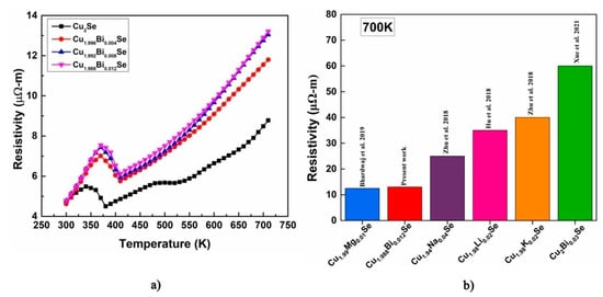
Figure 8.
(a) Temperature-dependent resistivity plot of Cu2−xBixSe (x = 0.00, 0.004, 0.008, 0.012) samples, (b) comparison of resistivity of the synthesized composition with existing literature on Cu2Se with different dopants [2,16,17,18,27].
Table 5.
Value of Resistivity, Seebeck coefficient, Power factor for Cu2−xBixSe (x = 0.00, 0.004, 0.008, 0.012) samples at 300 K.
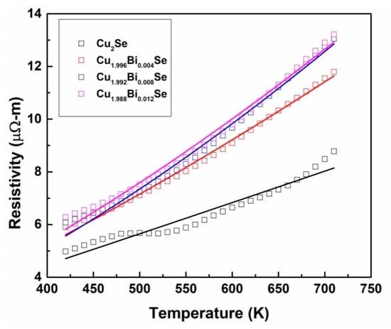
Figure 9.
Resistivity data fitted with Power law (Equation (9)).
Table 6.
Parameters obtained from power law (Equation (9)).
3.3.3. Seebeck Coefficient
The temperature-dependent Seebeck coefficient for Cu2−xBixSe (x = 0.00, 0.004, 0.008, 0.012) is measured in the temperature range 300–700 K. The variation is shown in Figure 10a. The positive sign of the Seebeck coefficient indicates that holes as dominant charge carriers which is confirmed with Hall measurements. It indicates that all the prepared samples are p-type semiconductors. The Seebeck coefficient of all the samples increases as the temperature rises, indicating the behavior of heavily doped semiconductors. With an increase in Bi concentration, the material's Seebeck coefficient increases due to the reduction in carrier concentration (See Figure 7) thereby verifying the Mott’s relation [28]. This trend is in agreement with the resistivity data. It shows that the dependency of carrier concentration is reflected in the nature of both the electrical resistivity and Seebeck coefficient. At room temperature, Seebeck coefficient for pristine sample is obtained as 49.5 μV/K which is in agreement with the reported values [29,30]. Room temperature Seebeck coefficient values of all the samples are listed in Table 5. Maximum Seebeck coefficient of 142 μV/K is obtained for the sample x = 0.012 at 700 K. Figure 10b represents comparison of Seebeck coefficient of synthesized Cu1.988Bi0.012Se to existing research on Cu2Se with various dopants.
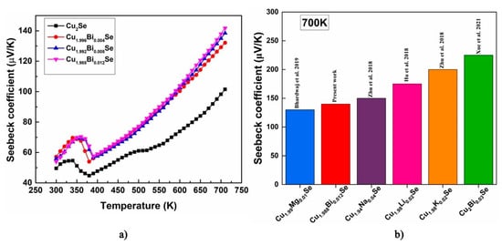
Figure 10.
(a) Temperature-dependent Seebeck coefficient for Cu2−xBixSe (x = 0.00, 0.004, 0.008, 0.012) samples, (b) comparison of Seebeck coefficient of the synthesized composition with existing literature on Cu2Se with different dopants [2,16,17,18,27].
3.3.4. Power Factor
The power factor of the Cu2−xBixSe is calculated in the temperature range 300–700 K by using the formula and represented in Figure 11a. The power factor of Cu2−xBixSe increases with an increase in Bi content. Enhancement in the thermopower is reflected in the power factor. It shows an increasing trend with increasing temperature. The highest power factor of 1474 μWm−1K−2 is observed at 700 K for the Cu1.988Bi0.012Se sample which is 30% higher than the pristine sample at 700 K. The power factor for the Cu2−xBixSe sample at 300 K is given in Table 5, and it can be observed that for Bi content x = 0.004 has the maximum power factor at room temperature. Due to high power factor Cu2−xBixSe can be considered as promising thermoelectric material. Comparison of power factor of the synthesized compound with existing research on Cu2Se with different dopants is represented in Figure 11b. It is observed that compared to other synthesized compounds present study has gained remarkable power factor.
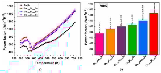
Figure 11.
(a) Temperature-dependent Power factor for Cu2−xBixSe (x = 0.00, 0.004, 0.008, 0.012) samples, (b) comparison of power factor of the synthesized composition with existing literature on Cu2Se with different dopants [1,16,17,18,27].
The comparison of power factors obtained from the current study and some previously studied compounds is given in Table 7. It provides the information about the power factor of various compounds which are prepared by different methods like solid state reaction technique, spark plasma sintering, hydrothermal method, high pressure synthesis, ball milling method etc. at 300 K and 700 K. The current study produced better outcomes than similar studies that have been published.
Table 7.
Comparing the power factor of various compounds.
4. Conclusions
Cu2−xBixSe (x = 0.00, 0.004, 0.008, 0.012) samples were prepared using the solid-state reaction technique with conventional sintering. From XRD data it is confirmed that Cu2−xBixSe has a monoclinic crystal structure and the space group changes from Cm to P21/c for pristine and doped samples respectively. All the samples exhibited less porous structures indicated the presence of well-connected grains. The resistivity of all the samples revealed phase transition at 350 K indicates the change in the structure from low temperature monoclinic to high temperature cubic. The positive value of Seebeck data confirms the p-type semiconductor nature with holes being the majority charge carriers. The resistivity and Seebeck coefficient of the sample increase with an increase in Bi content clearly indicates the dependency of carrier concentration. At 700 K, Cu1.988Bi0.012Se sample has the highest power factor of 1474 μWm−1K−2, which is 30% higher than the pristine sample at that temperature indicating that Bi-doped Cu2Se can be used as promising thermoelectric material for the thermoelectric applications.
Author Contributions
Conceptualization, P.P.; Methodology, A.A. and S.C.; Software, A., U.D.S., A.R. and S.C.; Validation, A.A., A.R. and S.C.; Formal analysis, C.P.B., A., A.A. and A.R.; Investigation, C.P.B. and P.P.; Data curation, U.D.S.; Writing—original draft, C.P.B.; Supervision, P.P.; Project administration, P.P. All authors have read and agreed to the published version of the manuscript.
Funding
This research received no external funding.
Data Availability Statement
The data presented in this study are available on request from the corresponding author.
Conflicts of Interest
The authors declare no conflict of interest.
References
- Mangavati, S.; Pal, A.; Rao, A.; Jiang, Z.-Z.; Kuo, Y.-K. Reduction in low-temperature thermal conductivity of Cu2Se via substitution of Se by Te atoms. J. Phys. Chem. Solids 2022, 160, 110301. [Google Scholar] [CrossRef]
- Xue, L.; Shen, W.; Zhang, Z.; Fang, C.; Zhang, Y.; Jia, X. Effects of Bi doping on thermoelectric properties of Cu2Se materials by high-pressure synthesis. Appl. Phys. A 2021, 127, 79. [Google Scholar] [CrossRef]
- Snyder, G.J.; Toberer, E.S. Complex thermoelectric materials. Nat. Mater. 2008, 7, 105–114. [Google Scholar] [CrossRef] [PubMed]
- Horike, S.; Wei, Q.; Akaike, K.; Kirihara, K.; Mukaida, M.; Koshiba, Y.; Ishida, K. Bicyclic-ring base doping induces n-type conduction in carbon nanotubes with outstanding thermal stability in air. Nat. Commun. 2022, 13, 3517. [Google Scholar] [CrossRef] [PubMed]
- Poudel, B.; Hao, Q.; Ma, Y.; Lan, Y.; Minnich, A.; Yu, B.; Yan, X.; Wang, D.; Muto, A.; Vashaee, D.; et al. High-thermoelectric performance of nanostructured bismuth antimony telluride bulk alloys. Science 2008, 320, 630–634. [Google Scholar] [CrossRef]
- Xie, W.; Tang, X.; Yan, Y.; Zhang, Q.; Tritt, T.M. Unique nanostructures and enhanced thermoelectric performance of melt-spun BiSbTe alloys. Appl. Phys. Lett. 2009, 94, 102111. [Google Scholar] [CrossRef]
- Joshi, G.; Yan, X.; Wang, H.; Liu, W.; Chen, G.; Ren, Z. Enhancement in Thermoelectric Figure-Of-Merit of an N-Type Half-Heusler Compound by the Nanocomposite Approach. Adv. Energy Mater. 2011, 1, 643–647. [Google Scholar] [CrossRef]
- Yan, X.; Liu, W.; Chen, S.; Wang, H.; Zhang, Q.; Chen, G.; Ren, Z. Thermoelectric property study of nanostructured p-type half-heuslers (Hf, Zr, Ti) CoSb0.8Sn0.2. Adv. Energy Mater. 2013, 3, 1195–1200. [Google Scholar] [CrossRef]
- Fu, T.; Yue, X.; Wu, H.; Fu, C.; Zhu, T.; Liu, X.; Hu, L.; Ying, P.; He, J.; Zhao, X. Enhanced thermoelectric performance of PbTe bulk materials with figure of merit zT & 2 by multi-functional alloying. J. Mater. 2016, 2, 141–149. [Google Scholar] [CrossRef]
- Heremans, J.P.; Jovovic, V.; Toberer, E.S.; Saramat, A.; Kurosaki, K.; Charoenphakdee, A.; Yamanaka, S.; Snyder, G.J. Enhancement of Thermoelectric Efficiency in PbTe by Distortion of the Electronic Density of States. Science 2008, 321, 554–557. [Google Scholar] [CrossRef]
- Zhao, L.-D.; Tan, G.; Hao, S.; He, J.; Pei, Y.; Chi, H.; Wang, H.; Gong, S.; Xu, H.; Dravid, V.P.; et al. Ultrahigh power factor and thermoelectric performance in hole-doped single-crystal SnSe. Science 2016, 351, 141–144. [Google Scholar] [CrossRef] [PubMed]
- Duong, A.; Nguyen, V.; Duvjir, G.; Duong, V.; Kwon, S.; Song, J.; Lee, J.; Lee, J.; Park, S.; Min, T.; et al. Achieving ZT = 2.2 with Bi-doped ntype SnSe single crystals. Nat. Commun. 2016, 7, 13713. [Google Scholar] [CrossRef] [PubMed]
- Benyahia, M.; Ohorodniichuk, V.; Leroy, E.; Dauscher, A.; Lenoir, B.; Alleno, E. High thermoelectric figure of merit in mesostructured In0.25Co4Sb12 n-type skutterudite. J. Alloys. Compd. 2018, 735, 1096–1104. [Google Scholar] [CrossRef]
- Ducka, A.; Trawiński, B.; Bochentyn, B.; Dubiel, A.; Kusz, B. Structure and thermoelectric properties of nickel-doped copper selenide synthesised in a hydrogen atmosphere. Mater. Res. Bull. 2020, 133, 111042. [Google Scholar] [CrossRef]
- Ballikaya, S.; Chi, H.; Salvador, J.R.; Uher, C. Thermoelectric Properties of Ag-Doped Cu2Se and Cu2Te. J. Mater. Chem. A 2013, 1, 12478. [Google Scholar] [CrossRef]
- Bhardwaj, R.; Bhattacharya, A.; Tyagi, K.; Gahtori, B.; Chauhan, N.S.; Vishwakarma, A.; Johari, K.K.; Bathula, S.; Auluck, S.; Dhar, A. Enhancement in thermoelectric performance of single step synthesized Mg doped Cu2Se: An experimental and theoretical study. Intermetallics 2019, 112, 106541. [Google Scholar] [CrossRef]
- Zhu, Z.; Zhang, Y.W.; Song, H.Z.; Li, X.J. Enhancement of the Thermoelectric Properties of Cu1.98Se by Na Doping. J. Electron. Mater. 2018, 47, 7514–7519. [Google Scholar] [CrossRef]
- Zhu, Z.; Zhang, Y.; Song, H.; Li, X.-J. Enhancement of thermoelectric performance of Cu2Se by K doping. Appl. Phys. A 2018, 124, 871. [Google Scholar] [CrossRef]
- Liao, W.-W.; Yang, L.; Chen, J.; Zhou, D.-L.; Qu, X.-L.; Zheng, K.; Han, G.; Zhou, J.-B.; Hong, M.; Chen, Z.-G. Realizing Bi-doped α-Cu2Se as a promising near-room-temperature thermoelectric material. Chem. Eng. J. 2019, 371, 593–599. [Google Scholar] [CrossRef]
- Geng, Z.; Shi, D.; Shi, L.; Li, Y.; Snyder, G.J.; Lam, K.-H. Conventional sintered Cu2-Se thermoelectric material. J. Materiomics 2019, 5, 626–633. [Google Scholar] [CrossRef]
- Bindu, P.; Thomas, S. Estimation of lattice strain in ZnO nanoparticles: X-ray peak profile analysis. J. Theor. Appl. Phys. 2014, 8, 123–134. [Google Scholar] [CrossRef]
- Monshi, A.; Foroughi, M.R.; Monshi, M.R. Modified Scherrer Equation to Estimate More Accurately Nano-Crystallite Size Using XRD. World J. Nano Sci. Eng. 2012, 2, 154–160. [Google Scholar] [CrossRef]
- Rabiei, M.; Palevicius, A.; Monshi, A.; Nasiri, S.; Vilkauskas, A.; Janusas, G. Comparing Methods for Calculating Nano Crystal Size of Natural Hydroxyapatite Using X-Ray Diffraction. Nanomaterials 2020, 10, 1627. [Google Scholar] [CrossRef] [PubMed]
- Zhang, T.; Song, Y.; Zhang, X.; He, X.; Jiang, J. Enhanced thermoelectric performance of Cu2Se by tuning the aligned lamella microstructure. Mater. Lett. 2019, 250, 189–192. [Google Scholar] [CrossRef]
- Thomas, R.; Rao, A.; Bhardwaj, R.; Wang, L.-Y.; Kuo, Y.-K. Reduction in Thermal Conductivity and Electrical Resistivity in Cu2SnSe3/Cu2Se Composite Thermoelectric System. Mater. Res. Bull. 2019, 120, 110607. [Google Scholar] [CrossRef]
- Mangavati, S.; Gurukrishna, K.; Rao, A.; Petwal, V.C.; Verma, V.P.; Dwivedi, J. Enhancement of Thermoelectric Power Factor in Cu2Se Superionic Conductor via High Energy Electron Beam Irradiation. J. Mater. Sci. Mater. Electron. 2023, 34, 1–10. [Google Scholar] [CrossRef]
- Hu, Q.; Zhu, Z.; Zhang, Y.; Li, X.-J.; Song, H.; Zhang, Y. Remarkably high thermoelectric performance of Cu2−XLiXSe bulks with nanopores. J. Mater. Chem. A 2018, 6, 23417–23424. [Google Scholar] [CrossRef]
- Gurukrishna, K.; Rao, A.; Jiang, Z.-Z.; Kuo, Y.-K. Enhancement of thermoelectric performance by tuning selenium content in the Cu2SnSe3 compound. Intermetallics 2020, 122, 106803. [Google Scholar] [CrossRef]
- Li, M.; Cortie, D.L.; Liu, J.; Yu, D.; Islam, S.M.K.N.; Zhao, L.; Mitchell, D.R.; Mole, R.A.; Cortie, M.B.; Dou, S.; et al. Ultra-High Thermoelectric Performance in Graphene Incorporated Cu2Se: Role of Mismatching Phonon Modes. Nano Energy 2018, 53, 993. [Google Scholar] [CrossRef]
- Zhao, L.; Islam, S.M.K.N.; Wang, J.; Cortie, D.L.; Wang, X.; Cheng, Z.; Wang, J.; Ye, N.; Dou, S.; Shi, X.; et al. Significant Enhancement of Figure-of-Merit in Carbon-Reinforced Cu2Se Nanocrystalline Solids. Nano Energy 2017, 41, 164. [Google Scholar] [CrossRef]
- Li, Y.; Wu, Z.; Lin, J.; Wang, Y.; Mao, J.; Xie, H.; Li, Z. Enhanced thermoelectric performance of hot-press Bi-doped n-type polycrystalline PbS. Mater. Sci. Semicond. Process. 2021, 121, 105393. [Google Scholar] [CrossRef]
- Kihoi, S.K.; Kahiu, J.N.; Kim, H.; Shenoy, U.S.; Bhat, D.K.; Yi, S.; Lee, H.S. Optimized Mn and Bi co-doping in SnTe based thermoelectric material: A case of band engineering and density of states tuning. J. Mater. Sci. Technol. 2021, 85, 76–86. [Google Scholar] [CrossRef]
- Zhao, L.; Yang, J.; Zou, Y.; Hu, J.; Liu, G.; Shao, H.; Zhang, X.; Shi, Z.; Hussain, S.; Qiao, G. Tuning Ag content to achieve high thermoelectric properties of Bi-doped p-type Cu3SbSe4-based materials. J. Alloy. Compd. 2021, 872, 159659. [Google Scholar] [CrossRef]
- Jiang, J.; Yang, C.; Niu, Y.; Song, J.; Wang, C. Enhanced Stability and Thermoelectric Performance in Cu1.85Se-Based Compounds. ACS Appl. Mater. Interfaces 2021, 13, 37862–37872. [Google Scholar] [CrossRef] [PubMed]
Disclaimer/Publisher’s Note: The statements, opinions and data contained in all publications are solely those of the individual author(s) and contributor(s) and not of MDPI and/or the editor(s). MDPI and/or the editor(s) disclaim responsibility for any injury to people or property resulting from any ideas, methods, instructions or products referred to in the content. |
© 2023 by the authors. Licensee MDPI, Basel, Switzerland. This article is an open access article distributed under the terms and conditions of the Creative Commons Attribution (CC BY) license (https://creativecommons.org/licenses/by/4.0/).