1. Introduction
Low-Dropout (LDO) regulators integrated on a chip are an essential part of modern microelectronic systems on chip (SoC). LDO regulators are especially required for internet of things (IoT) systems, where power is harvested from the environment (photovoltaic, thermoelectric or RF energy). In these applications, the regulators provide voltage stabilization regardless of the actual amount of acquired power. These regulators are also used in battery-powered mobile SoCs and complex analog-digital SoCs requiring clean supply voltages of different levels. In all these applications, the voltage drop across the regulator and the quiescent current should be as low as possible while maintaining good output voltage regulation and noise suppression. LDO regulators are often required to be completely integrated without the need for external capacitors, and capacitorless regulators are preferred for this reason [
1,
2,
3,
4,
5]. Designing LDO regulators for modern nanometer CMOS processes is becoming increasingly difficult due to the requirement of low supply voltage (less than 1 V) and short response time, which is required due to the high switching speed of powered circuits. In recent decades, this problem has been tried to be solved by using analog ALDO [
1,
2,
3,
4,
5,
6] or digital DLDO [
7,
8] low-dropout regulators. The designs of both types of regulators developed so far show that there is no single best solution. DLDO regulators are attractive because of their low-voltage operation, ease of automatic synthesis, and ability to be easily upgraded to modern technologies. On the other hand, the time response of DLDO regulators is relatively slow, especially in synchronous regulators. Additionally, these regulators have significant limitations in achieving good power supply rejection (PSR). For these reasons, DLDO regulators are mostly used to supply digital circuits where a certain level of supply voltage interference is tolerated. On the other hand, ALDO regulators allow greater suppression of interference and provide a better power-speed trade-off. However, these favorable features are increasingly difficult to maintain under low-voltage supply conditions. In ALDO regulators at low supply voltages, achieving sufficiently high gain necessary for strong noise suppression and good voltage regulation becomes very difficult. Similarly, the degradation of response time is a result of difficulty in generating large amplitude current pulses that enable the fast charging of parasitic capacitances. To overcome these difficulties, ALDO regulators in which the error amplifier is supplied with boosted voltage obtained by a charge pump have been proposed [
1,
2,
9,
10]. With such a solution, improvement in the operating conditions of the regulator is achieved at the cost of reduced power conversion efficiency and increased chip area.
This paper proposes the use of a native n-channel transistor and an effective circuit detecting output voltage spikes to generate strong current pulses, significantly reducing undershoots of the output voltage. Native or zero (near-zero) threshold voltage MOS transistors are available in many modern CMOS processes, and are used in ultra-low-voltage circuits [
11,
12]. Most often these are n-channel transistors with a threshold voltage close to zero or even negative. This very feature makes these transistors very attractive for application to low-voltage ALDO regulators. The main disadvantage of native transistors is relatively high channel length, which for technological reasons is about 2–4 times larger than in low-threshold voltage transistors. However, despite these limitations, the use of native transistors in ALDO regulators offers new opportunities that have not yet been exploited.
2. Problems Related to Low Supply Voltage of LDO Regulators
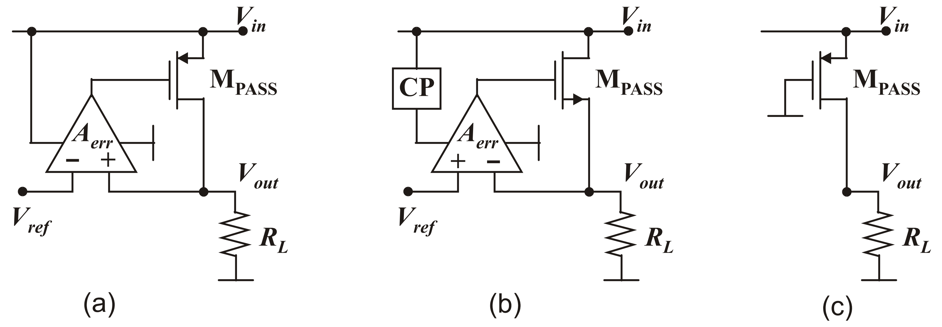
Figure 1 shows simplified configurations of the most commonly used LDO regulators [
1,
2].
Figure 1a,b shows ALDO regulators, while
Figure 1c shows a portion of a DLDO regulator for steady-state when the appropriate set of transistors in the array is turned on [
6]. In the regulator in
Figure 1b, with an n-channel pass transistor M
PASS, a charge pump (CP) is required to boost the voltage supplying the error amplifier (
Aerr) to provide sufficient voltage to control the gate of the n-channel transistor.
In ALDO regulators at low frequencies, PSR can be approximated by
where:
RL is a load resistance,
gds and
gm are the output conductance and transconductance of the pass transistor M
PASS,
Aerr is the voltage gain of the error amplifier, and
Aself =
gm/
gds is so called self-gain of M
PASS. Equation (1) was derived assuming that
Aerr and PSR of the error amplifier are high, and therefore the interference transfer from the amplifier supply voltage is negligibly small. In regulators of this type, the only way to improve PSR is by increasing the gain
Aerr of the error amplifier and increasing the self-gain
Aself of the pass transistor M
PASS. With a low voltage drop across the regulator and a large output current, the pass transistor enters the deep triode region, where the self-gain becomes very small. To compensate for the decrease in the self-gain, it becomes necessary to increase the gain of the error amplifier
Aerr, which in turn worsens the stability conditions of the control loop. In such a situation, sophisticated multi-loop methods of compensating the frequency characteristics of the error amplifier [
1,
13] become necessary. A side effect of such compensation is slowing down the time response of the regulator. In modern technologies, with low supply voltages, increasing voltage gain and implementing complex multi-loop compensation circuits become particularly difficult.
An even worse situation is in DLDO regulators (
Figure 1c), for which the PSR at low frequencies can be expressed as:
In this case, the PSR is relatively low, close to unity, in both regions of the pass transistor operation (triode and saturated). For this reason, hybrid analog-digital regulators [
1,
14], are often used to improve PSR and the time response.
From the Equation (1), it can be deduced that from the PSR improvement point of view, it is advantageous to use transistors that provide a high value of
Aself over the entire operating range.
Figure 2 shows
Aself plots for a low-threshold voltage p-channel transistor (p-MOS) and a native n-channel transistor (n-MOS) as a function of drain current. Both transistors are a parallel connection of 60 transistors, each with W = 100 µm channel width, which is equivalent to a single transistor with a channel width of W = 6000 µm. The minimum channel lengths for each transistor type were assumed, which for the selected process (X-FAB CMOS 180 nm) are respectively
L = 0.22 µm for the low-threshold voltage p-channel transistor and
L = 1 µm for the native n-channel transistor. It is worth noting that for the p-channel transistor, similar results are also obtained when the channel length is
L = 1 µm. These plots show that for both transistors,
Aself is relatively high in the saturation region (
ID < 5 mA) and decreases when the transistors enter the triode region (
ID > 5 mA). The advantage of the native n-MOS transistor is clearly evident, for which
Aself is higher, and thus the PSR that can be achieved in LDO regulator with such a transistor will be better.
At low supply voltages, it is very difficult to achieve good trade-off of stable frequency compensation and fast time response. As a result, large voltage undershoots and overshoots may appear at the regulator output when the output current changes rapidly. To better explain this problem, let us determine the equivalent impedance
ZG seen from the gate of the pass transistors M
PASS for the ALDO regulators shown in
Figure 1a,b. The schematics of the equivalent impedances for each configuration are shown in
Figure 3.
The calculations took into account the internal capacitances of the transistors (
Cgs and
Cgd) and the load resistances
RL connected to the regulator output. From these schematics, it is seen that a regulator with the pass transistor in a common-source configuration (
Figure 3a) has a much higher input capacitance resulting from the Miller effect. However, a much worse problem is the very large range of capacitance changes. The capacitance is relatively small when the transistor is in the triode region (
gmRL < 1), and increases many times when the transistor reaches the saturation (
gmRL >> 1). Such large variation of this capacitance makes the design of optimal frequency compensation much more difficult, and is the main cause of the response speed reduction. The situation is much more favorable in a regulator with the pass transistor M
PASS in a common drain configuration (
Figure 3b), where the capacitance seen from the gate is much smaller, and in addition, its variation is small (maximum change is approximately two times). Unfortunately, such a configuration can only be used with low supply voltage if the voltage supplying the error amplifier is boosted by means of a charge pump [
1,
9,
10], which in turn reduces the power conversion efficiency and increases chip area. The problem of using a pass transistor in a common drain configuration with a low supply voltage can alternatively be solved by using a native n-channel transistor. However, in order to avoid degradation of time response caused by longer channel of the native transistor, it is necessary to use effective circuits for output voltage spike suppression. Such circuits are needed to detect rapid spikes in output voltage and generate high amplitude current pulses to accelerate the response of the regulator.
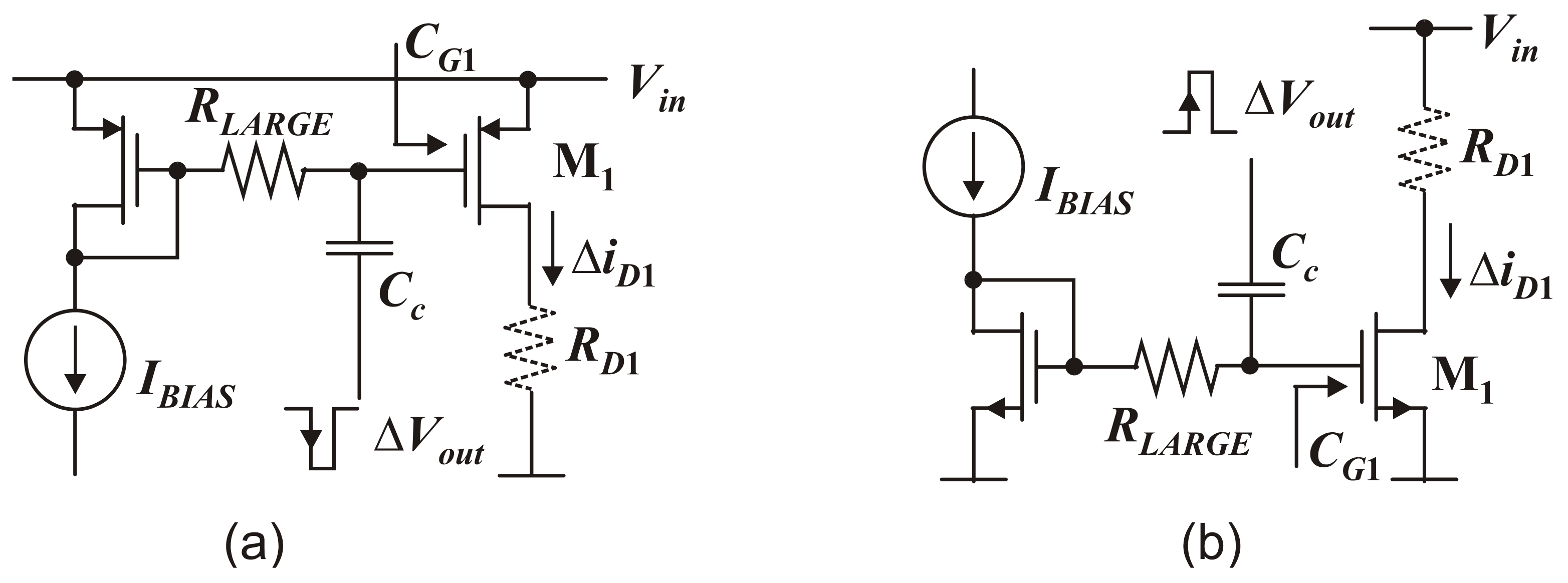
Figure 4 shows the spike detection circuits that are commonly used to reduce the response time of LDO regulators [
15,
16]. Each circuit detects a voltage spike Δ
Vout at the output of the regulator and generates a current pulse Δ
ID1 in response. Such a current pulse can be used to quickly charge the parasitic capacitance at the gate of the pass transistor M
PASS (
Figure 3).
The main advantage of these circuits is their simple design, though they are inefficient in operation and implementation. The amplitude of the current pulse generated by these circuits can be approximated by
where: Δ
Vout is the voltage spike at the output of the regulator,
Cc is the capacitance coupling the spike detection circuit with the regulator output,
Cgs1,
Cgd1 and
gm1 are the internal capacitances and transconductance of M
1 transistor, and
RD1 is affective resistance seen at the drain of M
1.
Based on Equation (3), it is apparent that, as in the circuit in
Figure 3a, the capacitance
CG1 seen from the gate of transistor M
1 is large due to the Miller effect. It is important to note that generation of high amplitude current pulse requires the use of M
1 with large transconductance
gm1, which means large channel width. Increasing the width of the channel leads to even larger capacitance
CG1, and thus requires a large capacitance
Cc occupying a large chip area. A more effective solution to this problem is presented in the next section.
3. ALDO Regulator with a Native n-MOS Transistor and Spike Detection Circuits
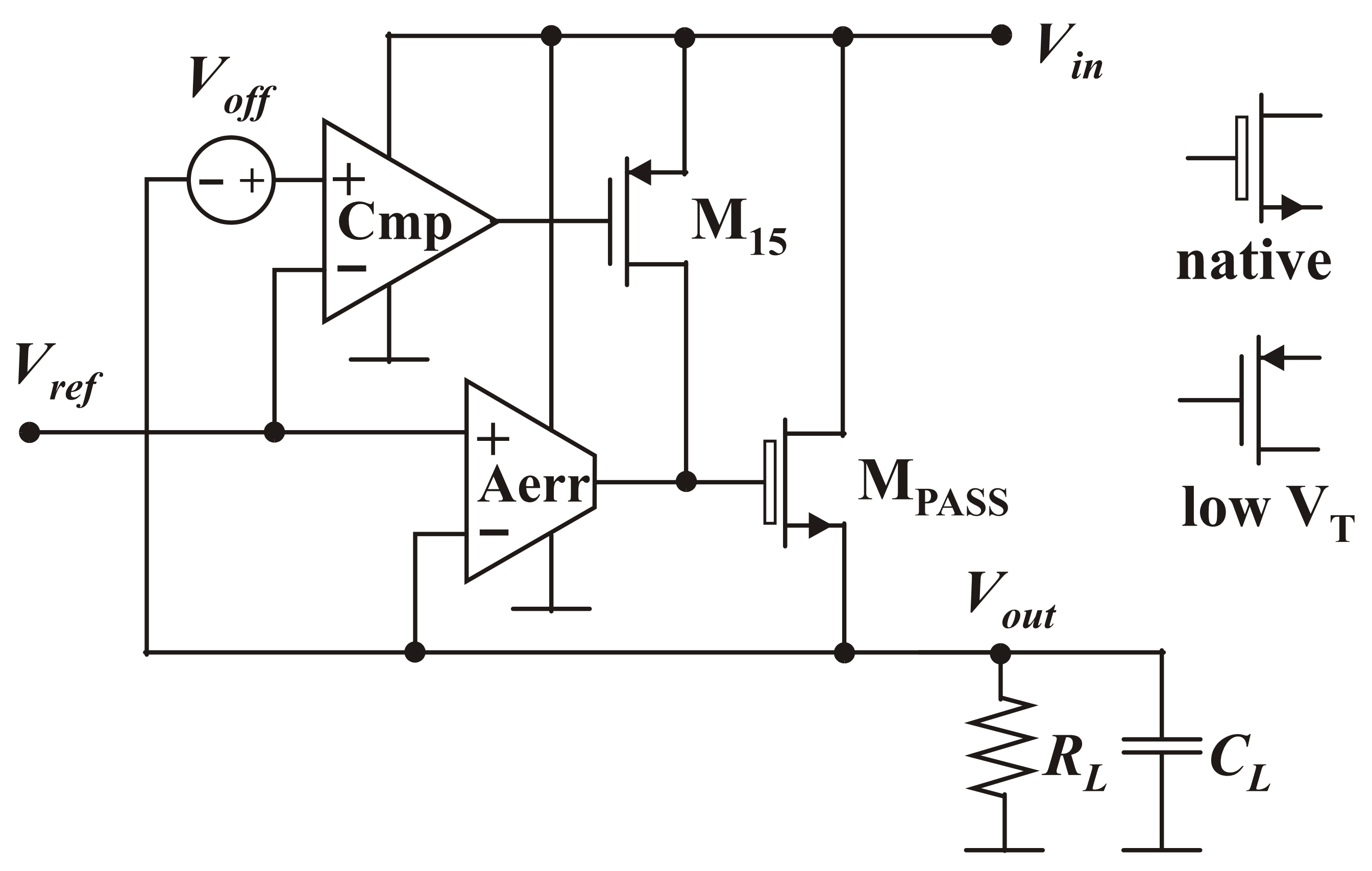
The general block diagram of the proposed ALDO regulator is shown in
Figure 5. The pass element is a native n-channel MOS transistor M
PASS, which is controlled by an error amplifier Aerr. Because of the low threshold voltage of M
PASS, the error amplifier Aerr can be directly supplied from the input voltage
Vin. In this regulator, an additional loop consisting of a comparator (Cmp) and an M
15 transistor is used to reduce output voltage undershoots. The comparator threshold voltage is shifted by
Voff below the required output voltage
Vout =
Vref. Therefore, when there is no
Vout undershoot, this loop is at idle and transistor M
15 is off. When
Vout drop occurs, the transistor M
15 is switched on only for a short time to reduce
Vout undershoot.
Figure 6 and
Figure 7 show two variants of the error amplifier (
Aerr), used for high (
Vout > 0.85 V) and low (0.7 <
Vout < 0.85 V) output voltages of ALDO regulator, respectively. Both amplifiers consist of two stages, the first being an input differential pair (M
1–M
3) with a cascode stage (M
4, M
5) and a dynamic load (M
6–M
9) and the second consisting of M
10–M
13 transistors. In the regulator for higher output voltages, there are additional voltage shifters (M
1A, M
3A, M
2A, M
3B), which increase the voltage drop across the cascode stage, and thus improves PSR and enables a smaller voltage drop across the pass transistor (M
PASS).
In the regulator for lower voltages, the inputs of the differential pair (M
1, M
2) are directly connected to the reference voltage
Vref and the regulator output
Vout. In this case, the available voltage drop across the cascode stage (M
4, M
5) is limited by the low supply voltage
Vin. For this reason, there is a slight degradation of PSR and the required voltage drop across the pass transistor (M
PASS) is higher.
Figure 8 shows the biasing circuit used in both regulators. This circuit generates the voltage V
B2, which is 0.8 V and 0.75 V for the high- and low-output voltage variants of the ALDO regulator. The bias currents of the particular amplifier stages were determined as a compromise between the minimization of the total power consumption and the speed of the transient response. The first amplifier stage consumes a current of 4 µA (4.4 µA with the voltage shifters), while the second stage consumes 10 µA. The highest current (8 µA) is consumed by a branch composed of transistors M
13 and M
12, so as to achieve a sufficient rate of discharging large input capacitance of the M
PASS transistor. The capacitor
C2, together with transistors M
11 and M
12, form a standard spike detection circuit (shown in
Figure 4b), and help reduce the regulator output voltage overshoots.
The compensation circuit of both error amplifiers includes capacitors
C1,
C2 and transistor M
4 acting as a current buffer. This is a simple and effective method of frequency compensation [
17,
18] that provides a relatively high phase margin which guarantees stable operation of the error amplifier and the complete ALDO regulator. More details about compensation and stability will be given when analyzing the negative feedback loop of the complete regulator.
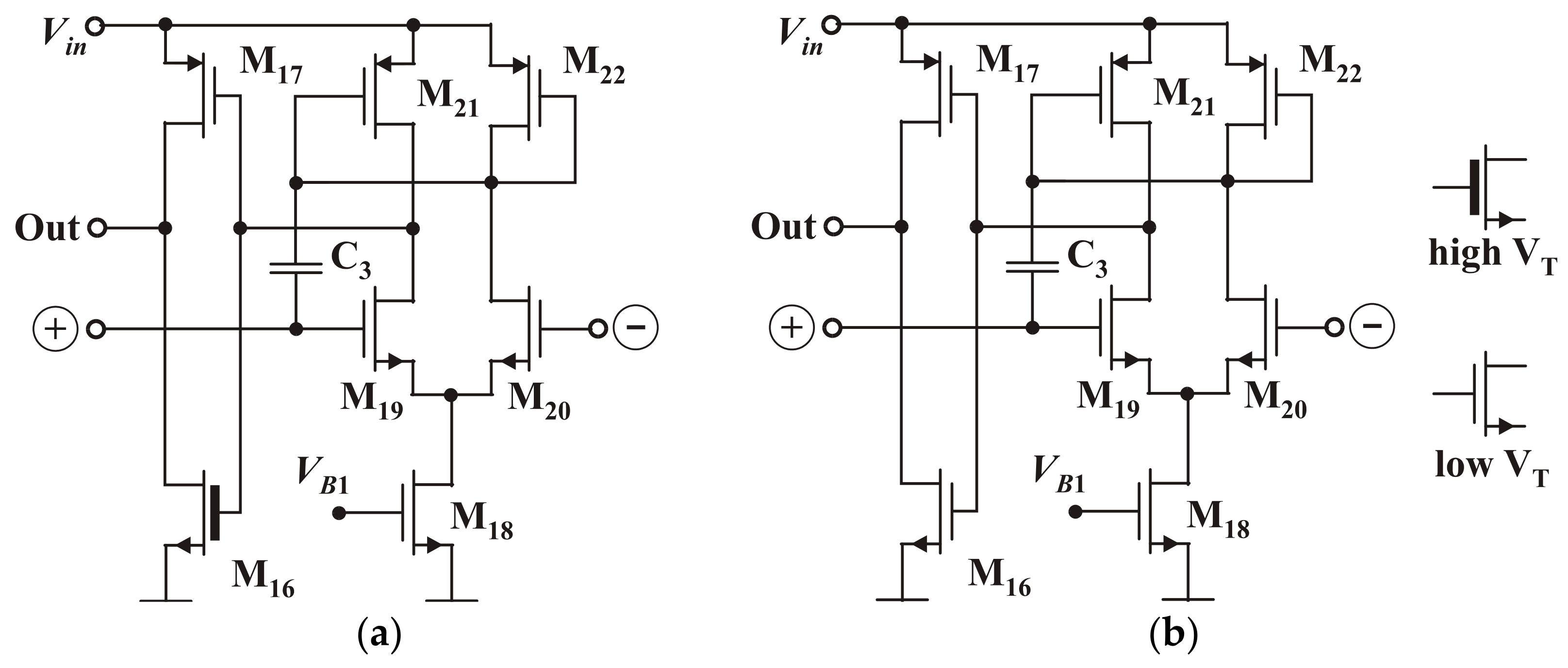
Figure 9 shows a schematic of the comparator (Cmp) used in the output voltage undershoots suppression loop, depicted in
Figure 5. It is a classical comparator consisting of an input differential pair (M
19, M
20) with a dynamic load (M
21, M
22) and an output inverter (M
16, M
17). The comparator was deliberately unbalanced to achieve an offset voltage
Voff = 10 mV to protects the suppression loop from generating series of pulses that could destabilize ALDO regulator during transients. The offset voltage is achieved by increasing the channel width of the transistor M
19 by 50% compared to M
20. To accelerate the switching of the comparator, the capacitor C
3 was added to increase the peak drain current of the transistor M
21 during
Vout undershoots. With the high gain of the comparator, it is possible to generate high-current pulses using a small-size M
15 transistor, and as a result reduce the regulator output voltage undershoots. The static current consumption of the comparator is 2 µA.
Complete schematics of ALDO regulators are shown in
Figure 10 and
Figure 11, where the undershoot detection circuit is surrounded by a dashed line. The frequency characteristics of the negative loop are mainly determined by 5 poles and one transmission zero, which are associated with the nodes labeled A–E.
Based on the method described in [
17,
18], the approximated equations describing the poles and zero were determined
where:
Equation (4) defines the dominant pole
pD. The effect of poles
p2 and
p4 on stability can be neglected, because they are always well above the unity-gain bandwidth (UGB), which is approximately UGB ≈
gm1/
C1, while
CB <<
C1,
CE <<
C1 and
CE <<
C2. The stability conditions are most influenced by the
p3 and
p5 poles, with the position depending on the gate capacitance
CC and transconductance
gmPASS of the pass transistor M
PASS and the load capacitance
CL, connected to the regulator output. The most critical conditions occur when the capacitance
CL is large and the output current
Iout is low, and therefore
gmPASS is small. Under such conditions, both poles approach the UGB reducing the phase margin. In the presented ALDO regulator, the position of the dominant pole (4) and consequently the UGB was adjusted by selecting
C1 = 1.8 pF to achieve the worst-case phase margin greater than 45 degrees. Details of the circuits in
Figure 10 and
Figure 11 are given in
Table 1.
4. Results of LDO Regulator Simulations
Properties of the regulators shown in
Figure 10 and
Figure 11 were verified by a series of simulations performed using the Spectre simulator from the Cadence package.
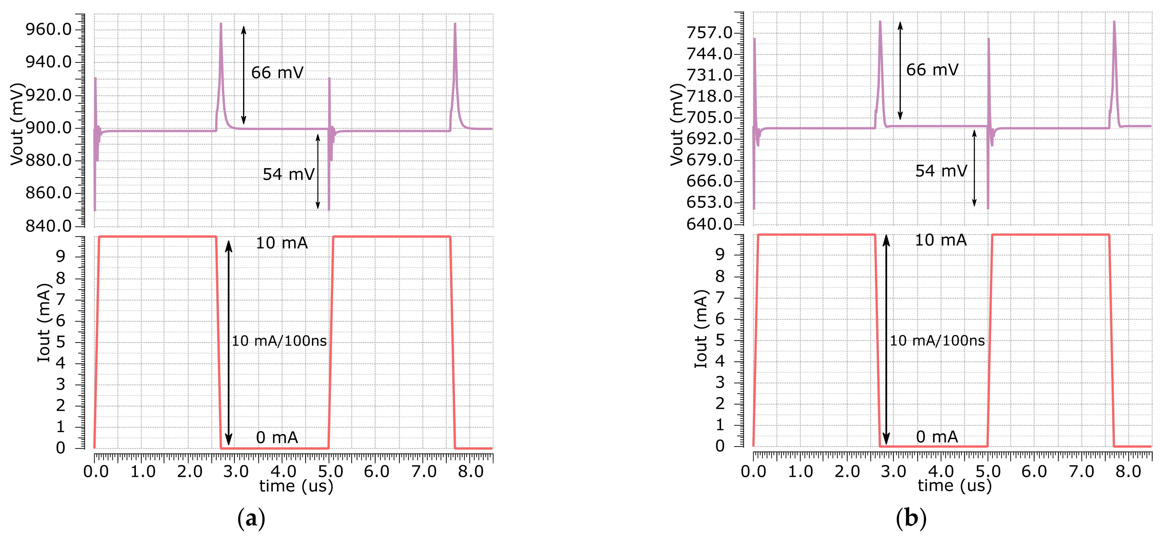
Figure 12 shows the time responses of ALDO regulators with the output voltage
Vout = 0.9 V and 0.7 V, when the output current changes between 0 and 10 mA with the rise and fall times of 100 ns. The dropout voltage is
Vdrop = 80 mV for the
Vout = 0.9 V regulator and
Vdrop=100 mV for the
Vout = 0.7 V regulator. From the figure, it can be seen the overshoot and undershoot with amplitudes +Δ
Vout = 66 mV and −Δ
Vout = 54 mV for
Vout = 0.9 V and
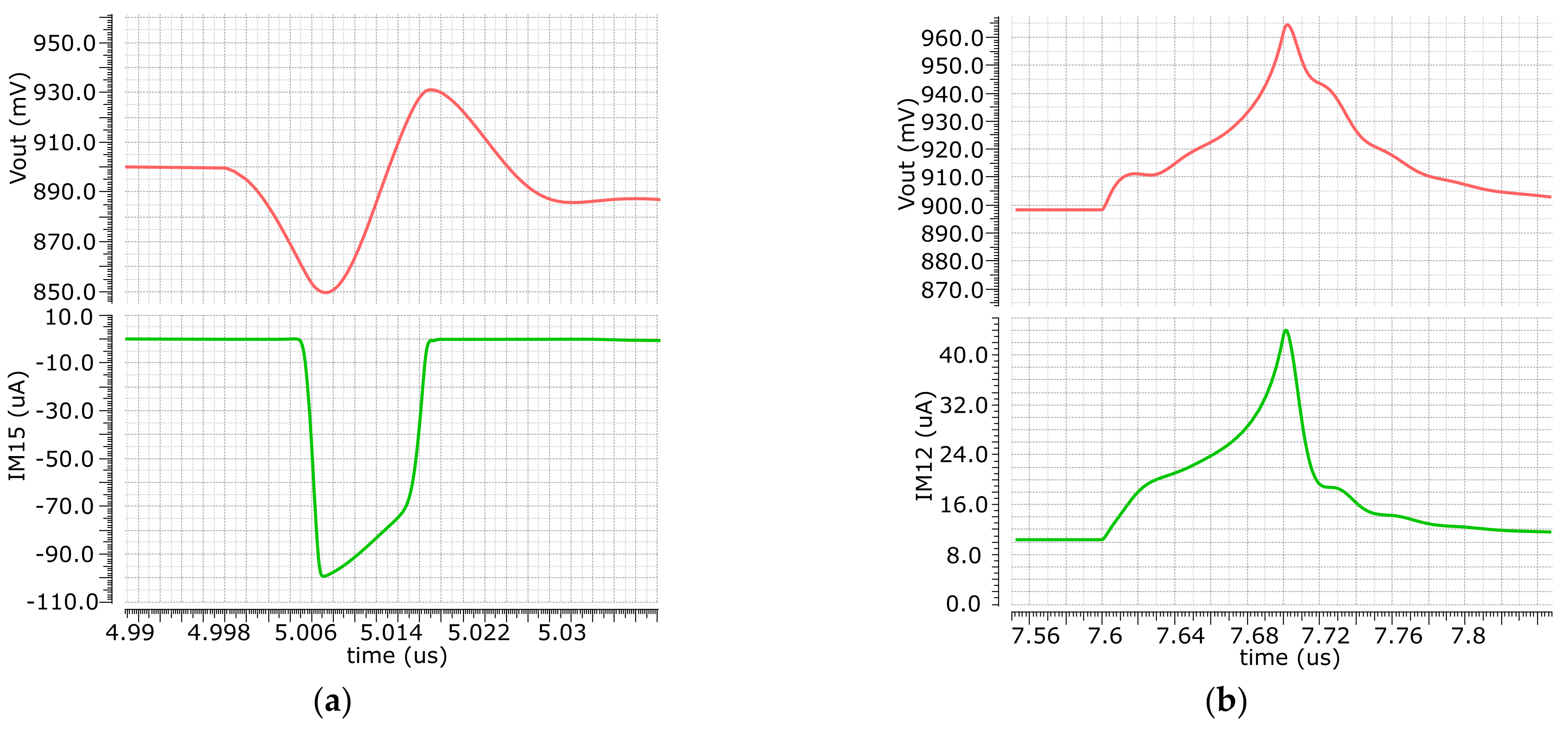
Vout = 0.7 V regulator. Magnified sections of the
Vout plot showing details of voltage spikes for
Vout = 0.9 V regulator are presented in
Figure 13. These plots also show the drain currents of the transistors M
15 and M
12.
Figure 13a shows the moment when the voltage
Vout drops below the comparator threshold voltage, and at this time the transistor M
15 generates a high-current pulse with short rise and fall times, which quickly charges the input capacitance of the pass transistor M
PASS, causing a significant reduction in the output voltage undershoot. Note that due to the delay in switching off the comparator, a parasitic voltage overshoot of about 30 mV amplitude is also generated.
Figure 13b shows the details of
Vout overshoot. In this case, the current pulse generated by M
12 is approximately two times smaller in amplitude and has much longer rise and fall times, resulting in a wider overshoot of
Vout. In this regulator, only the simpler solution shown in
Figure 4b was used to suppress overshoots, due to the main effort to reduce the total quiescent current. If a stronger overshoot reduction is required, a comparator-based spike suppression circuit can also be used.
Plots of PSR as a function of frequency for selected values of the output current
Iout (0, 2.5 mA, 5 mA, 7.5 mA, 10 mA) are shown in
Figure 10. The plot in
Figure 14a shows the characteristics of the regulator with a native transistor (
Figure 10). For comparison,
Figure 14b shows PSR characteristics of an analogous regulator with a low-threshold voltage p-channel pass transistor (M
PASS). This regulator was created on the basis of the schematic in
Figure 10 by swapping the inputs of the differential pair (M
1, M
2) and adjusting capacitances (
C1 = 3 pF,
C2 = 0) to achieve stable operation.
Figure 14a shows that at low frequencies, PSR reaches the highest value for the smallest current (0 mA), which is 61.5 dB and 43 dB for the regulator with the native n-channel and p-channel transistors, respectively. PSR decreases to 46.5 dB for the regulator with the native n-channel transistor when the current increases to 10 mA. Even in this case, PSR is about 6 dB better than the value obtained for the regulator with the p-channel transistor.
For the regulator with the output voltage
Vout = 0.9 V, the smallest phase margin is 75 degrees for
Iout = 0 mA and
CL = 500 pF, whereas the highest margin is 101 degrees for
Iout = 0 mA and
CL = 5 pF. For all intermediate values in the range
Iout = 0–10 mA and
CL = 0–500 pF, the feedback loop is stable with the phase margin greater than 75 degrees, and the unity-gain bandwidth in the range of 2–5 MHz.
Figure 16 shows the amplitude-phase frequency characteristics of the low-voltage version of the regulator (
Figure 11) for
Vout = 0.7 V. In this case, the smallest phase margin is 45 degrees for
Iout = 0 mA and
CL = 500 pF and the highest is 77 degrees for
Iout = 0 mA and
CL = 5 pF. Furthermore, in this case, the regulator is stable for all values in the range
Iout = 0–10 mA and
CL = 0–500 pF, with the unity-gain bandwidth in the range of 1.8–4 MHz.
A summary of the most important parameters of the proposed LDO regulator along with the values obtained for the process corners (slow nMOS & pMOS transistors, temperature 0 °C or 50 °C) is summarized in
Table 2. In the worst-case corner, the voltage regulator with
Vout = 0.9 V can operate with a minimal drop voltage of 90 mV with output voltage spikes of less than 70 mV and PSR = 38 dB. The low-voltage version of the regulator, when supplied with
Vin = 0.8 V, provides an output voltage of
Vout = 0.7 V with a slightly worse PSR = 35 dB.
The influence of technology parameter variation and component mismatch is illustrated in
Figure 17. The plots show the amplitude and phase characteristics of the control loop for 100 Monte Carlo analysis runs. These results show that the gain of the control loop may change from 36 dB to 47 dB, while the phase margin varies from 97 to 110 degrees. Such a range of changes will not result in a loss of loop stability, but may result in about 50% deterioration of parameters such as line regulation or the regulator output resistance.
5. Comparison to The State-of-the-Art and Conclusions
The simulation results of the parameters obtained in the proposed voltage regulator were compared with the measurement results of similar solutions described in the literature. A comparative summary is provided in
Table 3. The proposed regulator, compared to the regulator with p-channel pass transistor [
3] designed in similar 180 nm technology, has a smaller voltage drop
Vdrop, a smaller total on-chip capacitance, and a better response speed, as it is indicated by a smaller FOM and a shorter settling time. Compared to the charge-pump based regulators [
10,
19], the proposed regulator is better in power efficiency
η and has a much smaller total on-chip capacitance. The regulator with a hybrid configuration (ALDO + DLDO) [
6] features a very low quiescent current, high efficiency and relatively fast response, though these favorable characteristics were obtained due to a large voltage drop
Vdrop = 300 mV, large total on-chip capacitance 220 pF and a relatively high output voltage
Vout = 2.7–3.3 V, which can be a significant limitation in low-voltage circuits. ALDO regulators described in papers [
4,
5,
20] use low-voltage p-MOS pass transistors and are designed for low output voltages (0.6 V−0.9 V). Comparing the parameters of these regulators with the proposed regulator, it is seen that the proposed regulator is more favorable in terms of minimum dropout voltage (100 mV versus 150–200 mV). In the solution [
20], a particularly low quiescent current (16 nA) was obtained, but this was achieved at the cost of a large (1 µF) off-chip capacitor and degraded transient response (FOM = 0.11). The regulators [
4,
5] have a favorable transient response, though they require a relatively high quiescent current (112 µA and 65 µA). It should also be noted that in implementations of regulators [
4,
6,
19], the output current must not be less than the minimum value (100 µA, 10 µA, 120 µA), otherwise the regulator may lose stability. The proposed regulator is free from this limitation, which is particularly severe in SoCs with implemented sleep function. This comparison shows that the proposed regulator allows to achieve a satisfactory compromise of parameters important for SoCs powered with a voltage below 1 V.
In this paper, a low-voltage ALDO regulator based on a native n-MOS transistor as a pass element is proposed as a promising alternative to known solutions. In such a regulator, the pass transistor can operate in a common drain configuration, which improves the circuit performance and simplifies its design. The fact that the native transistor, depending on the technology used, has a threshold voltage close to zero or even negative eliminates the need for a charge pump boosting the voltage supplying the error amplifier. Elimination of the charge pump avoids the use of relatively large on-chip capacitors necessary for the pump operation.
The total capacitance used in such pumps can reach several hundred pF, which is a major disadvantage of this type of solution. The proposed regulator under low-voltage conditions allows obtaining satisfactory parameters as compared to the regulators with charge pumps, and classical regulators with a p-channel transistor as a pass element. It is worth noting that the proposed regulator allows to push the limit of application of ALDO regulators to voltages below 1 V with only slight degradation of output voltage spikes, response speed and PSR, which is very difficult to achieve in previously known solutions.


