Review

How to Achieve Efficiencies beyond 22.1% for CdTe-Based Thin-Film Solar Cells

Thin Film Research Centre, Industrial & Innovation Research Institute, Sheffield Hallam University, Sheffield S1 1WB, UK
*
Author to whom correspondence should be addressed.
Energies 2022, 15(24), 9510; https://doi.org/10.3390/en15249510
Submission received: 4 November 2022 / Revised: 3 December 2022 / Accepted: 12 December 2022 / Published: 15 December 2022
(This article belongs to the Topic Photovoltaic Materials and Devices)

Abstract

:
This review paper summarises the key issues of CdTe and CdS/CdTe solar cells as observed over the past four decades, and focuses on two growth techniques, electrodeposition (ED) and closed space sublimation (CSS), which have successfully passed through the commercialisation process. Comprehensive experience in electrical contacts to CdTe, surfaces & interfaces, electroplated CdTe and solar cell development work led to the design and experimentally test grading of band gap multilayer solar cells, which has been applied to the CdS/CdTe structure. This paper presents the consistent and reproducible results learned through electroplated CdTe and devices, and suggestions are made for achieving or surpassing the record efficiency of 22.1% using the CSS material growth technique.

1. Introduction

Photovoltaic (PV) energy conversion is an excellent method for generating clean energy; however, most of the research and commercialisation since the early 1950s has focused on the well-explored semiconducting material, silicon (Si). About 85% of the PV market today is covered by crystalline and poly-crystalline Si solar cells. After the first oil crisis in the early 1970s, scientists extended their active research towards thin-film solar cells in order to reduce material use and manufacturing costs. Over the next three decades, research focused on solar cells based on CdTe, CuInGaSe2 (CIGS) and dye-sensitised solar cells (DSSCs). Researchers are continuously exploring non-toxic, earth-abundant, and low-cost materials to develop high efficiency solar cells for the future. Kesterites and Perovskites are two such materials under vigorous research at present.
Research into CdTe- and CIGS-based thin-film solar cells have progressed well, and both entered into the scaling-up and commercialisation stages in the 1980s. Two-element CdTe-based solar cell work was comparatively easier than four-element CIGS-based solar cells, due to difficulties in handling several elements and reproducibility issues. For these reasons, CdTe commercialisation work has been successful and has entered into the PV market. Commercialisation of CdTe-based solar cells in the 1980’s by BP Solar using electroplated CdTe was successful, and by ~2000, this programme produced solar panels of about 1.0 m2 with ~11% module efficiencies at a full-scale production line in the US [1]. However, the termination of most of the solar energy work around 2002 by BP Solar was a significant setback for thin-film solar panel research and development based on CdTe.
Many research groups world-wide continued their research in academic environments, but the small lab-scale devices achieved only about 15–16% [2,3]. This efficiency stagnated for about two decades without further improvements, although researchers used about 14 different growth techniques to grow CdTe [4]. A US-based research group was also continuously researching CdTe-based solar cells using the close-spaced sublimation (CSS) growth technique. This group later scaled up the process and finally became First Solar, producing large area solar panels. Around 2016, First Solar announced a record efficiency of ~22.1%, with CdTe grown by a modified CSS method [5]. The stability of CdTe-based solar cells is excellent, and the work by First Solar represents the most successful manufacturing of thin-film solar panels. Since this work has been carried out under commercial confidentiality, understandably, scientific details are not available to the research community. During the past six years, there was no reporting of any other efficiency improvement for this device.
Although a large number of growth techniques have been used to grow CdTe [4], only two methods, electrodeposition and CSS, have successfully passed through the scaling-up and commercialisation programme. Therefore, this article focuses only on these two growth techniques, although the ideas can be used for any other CdTe growth methods. The CdS/CdTe solar cell has been a complex subject over the past five decades, but now most of the scientific information is coming together for improved understanding of the material and device issues [6,7,8]. However, the most of important information is hidden in the scientific literature, and is difficult to extract in order to streamline future research. The first author (IMD) of this article has been researching in this field, covering both materials and devices, for over four decades in both industrial and academic environments. The primary growth technique used over this time was electrodeposition, and both materials and device issues around this system were investigated. The main aim of this review article is to filter the most relevant information into one document to facilitate future research on these devices, with a view to achieving or even surpassing the record efficiency of 22.1%.
In order to support the new researchers entering this field, the main stages of fabrication of a typical CdS/CdTe solar cell are summarised in Figure 1. The substrate used for the device is commercially available glass/FTO (fluorine-doped tin oxide) with a sheet resistance of 7 Ω/square and the first stage is to thoroughly clean the surface using soap, water, acetone, methanol and high purity water. The second stage is the deposition of the CdS window layer by either chemical bath deposition (CBD) or electroplating. Researchers have also used other methods, such as sputtering, to deposit the CdS layer, and its thickness is in the range 50 nm to 100 nm. This layer requires annealing in air at 400 °C for ~20 min. After cleaning the CdS surface using an alkaline etch to remove any oxides formed during heat treatment, the CdTe absorber layer is deposited. The thickness of the CdTe layer depends on the growth method used; electrodeposition results in a layer thickness of ~1.5–2.0 µm, while the CSS method results in a layer thickness in the range of ~3.0–8.0 µm. This layer then undergoes a heat treatment in air at ~420 °C for ~20 min in the presence of CdCl2; this is the so-called CdCl2 treatment. The resultant surface then undergoes thorough washing in clean water to remove traces of CdCl2, and a suitable chemical etching prior to metallisation. Figure 1 shows the chemical etching used in our labs, and this process creates a Cd-rich CdTe surface. There are other chemical etchants, such as the NP etch (nitric acid & phosphoric acid) also used by other research groups. Back metal contact is usually Au or Ni with a trace of Cu or Sb to enhance the initial efficiency of the device. The specification of the device with typical material layer thicknesses used in electroplating are also included in Figure 1.

2. Experimental Evidence

The focus of the first author’s work on semiconductor growth has been using electrodeposition, with over 18 different electronic materials being explored to date [6,7]. CdTe was the primary focus, and the various properties of the materials and their impact on PV devices was studied. Before the ways forward are discussed, this section collates the most important experimental evidence observed and reported in the literature.

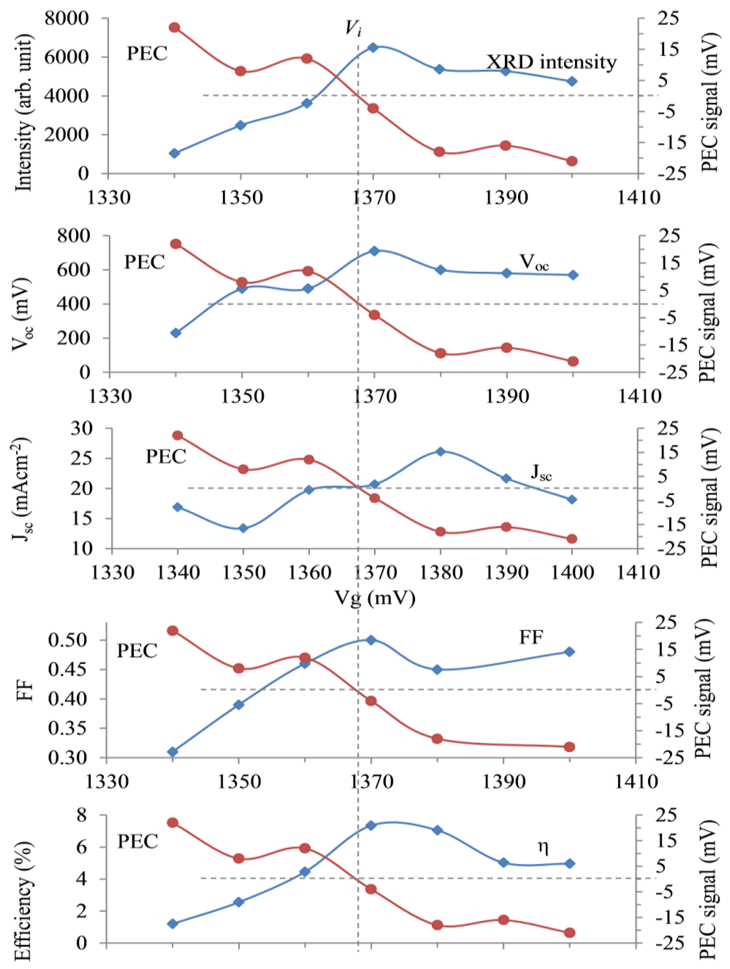
2.1. Intrinsic Doping of CdTe

Electrodeposition of CdTe is usually carried out with an aqueous electrolyte containing cadmium and tellurium ions. Cadmium ions and tellurium ions are provided by dissolving a Cd compound (sulphate, nitrate or chloride) or TeO2 in high purity water, respectively. Materials are grown at ~85 °C on glass/FTO substrates. Figure 2 shows [8] the summary of the typical material properties of the electroplated CdTe layers after heat treatment in the presence of CdCl2. These results were obtained using the two-electrode system, thereby avoiding detrimental contamination by potassium (K) from the outer jacket of the reference electrodes. Traces of group-I elements in ppb level can drastically reduce the efficiency of CdS/CdTe solar cells fabricated with electroplated CdTe [9]. Vg in the X-axis is the growth voltage or the voltage applied between the anode and the cathode. In this system, Te deposits easily at low cathodic voltages, and Cd needs larger cathodic voltages for discharge and deposition. Therefore, at low Vg values, the layers are Te-rich, while at higher Vg values, the layers are Cd-rich in composition. At an intermediate i-point at 1.576 V, for this particular electrolyte, stoichiometric CdTe can be grown. The curve A in Figure 2 indicates the intensity of the most intense (111) XRD peak as a function of Vg. When the material is stoichiometric, peak intensity is highest indicating the best crystallinity of the layers. This intensity suffers when Vg is away from the i-point due to the existence of two phases, CdTe + Te at low Vg values and CdTe + Cd at high Vg values. Because of the presence of the two phases, the crystalline nature of the material is diminished.
A photo–electrochemical (PEC) cell was used to determine the electrical conduction type of the electroplated CdTe layers, since the conventional Hall effect technique cannot be used due to the underlying conducting layer of FTO. Curve B in Figure 2 shows the variation in the PEC signal as a function of Vg for electroplated and CdCl2-treated material. At cathodic voltages below the i-point, the material is rich in Te and the PEC signals are positive, indicating that the CdTe layers are p-type. At cathodic voltages above i-point, the material is rich in Cd and the PEC signals are negative; indicating the CdTe layers are n-type in electrical conduction. The curve C-i-C’ (Figure 2) therefore indicates the variation in possible doping concentrations. In order to keep the high crystallinity and moderate doping ~(1014–1015 cm−3) that are needed for device fabrication, the layers should be grown close to the i-point. Figure 2 also lists the possible defects in these two types of CdTe layers. Obviously, one defect set will be more dominant than the other, as we can experimentally observe using photoluminescence (PL) measurements in later sections.
This phenomenon of intrinsic doping has also been observed for CSS- [10] and modified CSS- (vapour transport deposition) [11] grown CdTe thin-films in previous studies. Similarly, to that of the electroplating, CSS-grown CdTe has also been shown a transition from p-type to n-type, depending on the composition of the films (Cd/Te ratio), where Te-rich CdTe exhibited p-type and Cd-rich CdTe exhibited n-type electrical conductivity. It is important to note that the Te-richness and Cd-richness need only occur in the ppm level to change the electrical conduction. However, in the above two reported works, the Cd/Te ratio was in the level of percentages, and hence drastically affected the crystallinity of the resultant layers (see curve “A” in Figure 2). These structural changes will severely affect the device performance. Therefore, for high-efficiency devices, both the crystallinity and moderate doping should be achieved by growing the material close to the stoichiometry, but only on the Cd-rich side.
(i). 
Composition of CdTe is highly sensitive and depends on the growth conditions used.
(ii). 
Intrinsic doping by variation in composition is possible for CdTe layers. Te-rich CdTe produces p-type material, and Cd-rich CdTe produces n-type material.

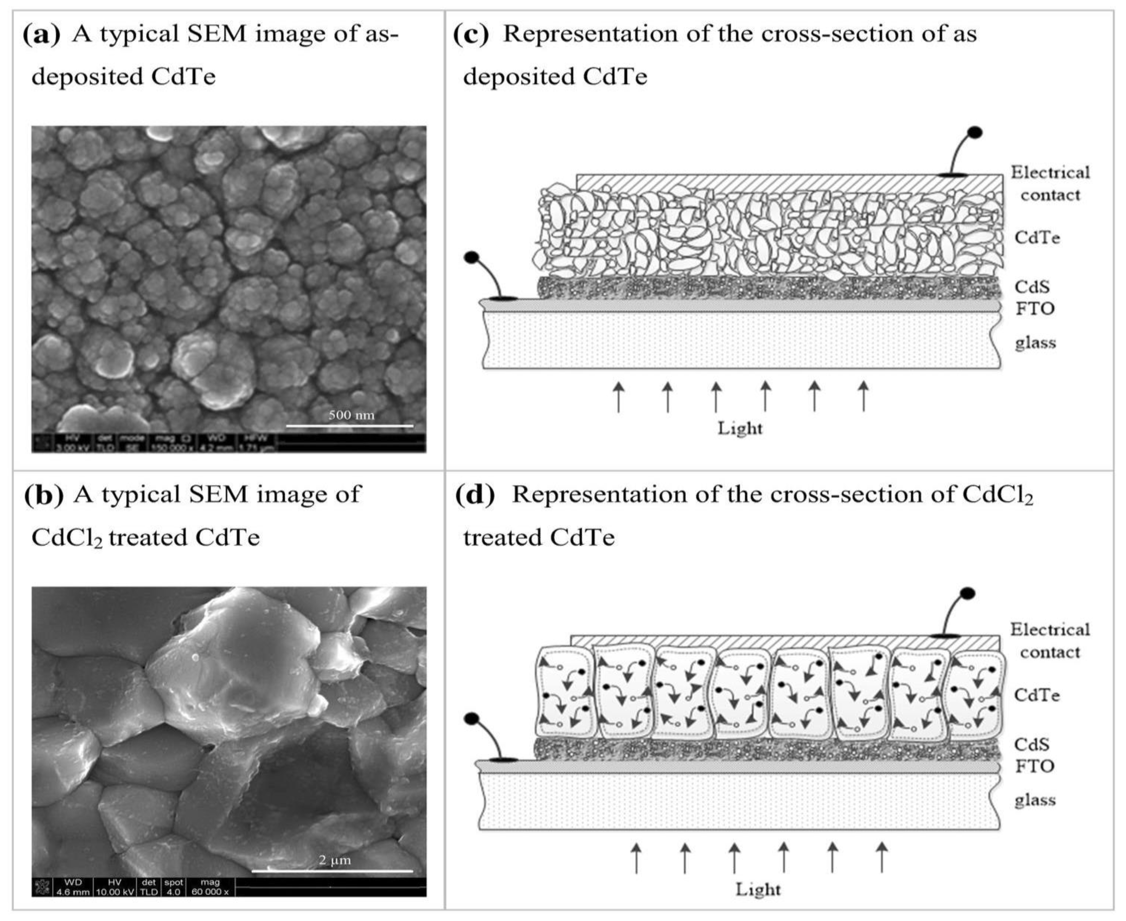
2.2. Material Improvement by CdCl2 Treatment

As deposited CdTe layers at low temperature (~85 °C) are not suitable for device fabrication, their PV conversion efficiencies are either very low or almost zero. The need for heat treatment in air using CdCl2 has been known for a long time [12]. This step drastically improved the solar cell efficiency, but the underlying science was not understood for a long time. For this reason, the CdCl2 treatment step was reported as a “magic step” by some scientists [13]. CdCl2 treatment has also been carried out using many different methods. Common practice was to dip the layers in a solution containing CdCl2 dissolved in water or methanol, dry the layer and then heat-treat it at an elevated temperature [14]. Some groups deposited a thick layer of solid CdCl2 before heat treatment [15,16]. Another method was to expose the layers to halide-containing gas (HCF2Cl) at high temperatures [17]. Heat-treatment temperature also varied from ~350–450 °C. Although the science behind this crucial step was not understood for a long time, careful research over the past few decades has now improved the understanding of this processing step [14].
Whatever the growth technique used for CdTe, it has been reported that the layers suffer from Te-richness. Te also tends to precipitate within CdTe, impacting the stoichiometry. This is an inherent problem with CdTe material, irrespective of the growth technique [18]. Recent XRD and Raman work, as shown in Figure 3, indicates the presence of Te in the as-deposited material and the removal of the excess Te during CdCl2 treatment [19]. Added Cd from CdCl2 reacts with precipitated Te to form CdTe during this heat treatment, improving the stoichiometry and moving the material towards Cd-richness, thus making the material more suitable for device fabrication (see Section 2.6). In addition, XRD shows the improvement of the crystallinity of the material.
There are numerous examples in the literature showing improvement of crystal growth after CdCl2 treatment [20,21,22]. Figure 4 shows typical SEM images of electro-plated CdTe layers and CdCl2-treated CdTe layers. As deposited CdTe shows small crystallites ~20–65 nm in large clusters or agglomerations. During the CdCl2 treatment, these crystals fuse together to form large crystals or grains of a few microns in size. Various reports show that these form columnar-type large crystals extending across the whole thin-film layer. Figure 4c,d illustrate the visualisation of cross-sections based on SEM and TEM observations.
CdCl2 treatment:
(i). 
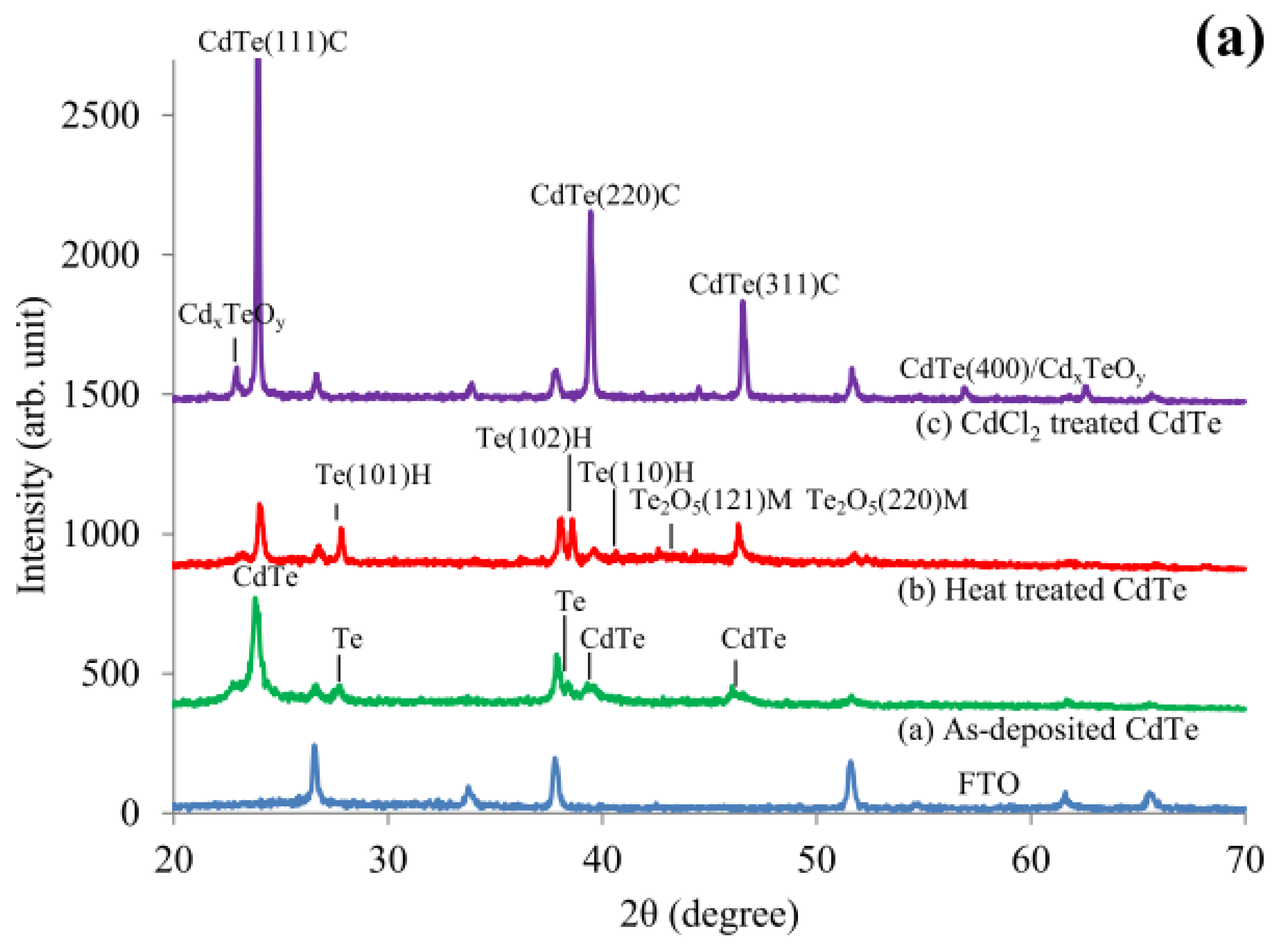
removes any precipitated and excess Te from the CdTe layers, improving stoichiometry, and can even shift the composition towards Cd-rich CdTe layers;
(ii). 
improves crystal growth, and forms large columnar type crystals extending from front to rear of the device structure;
(iii). 
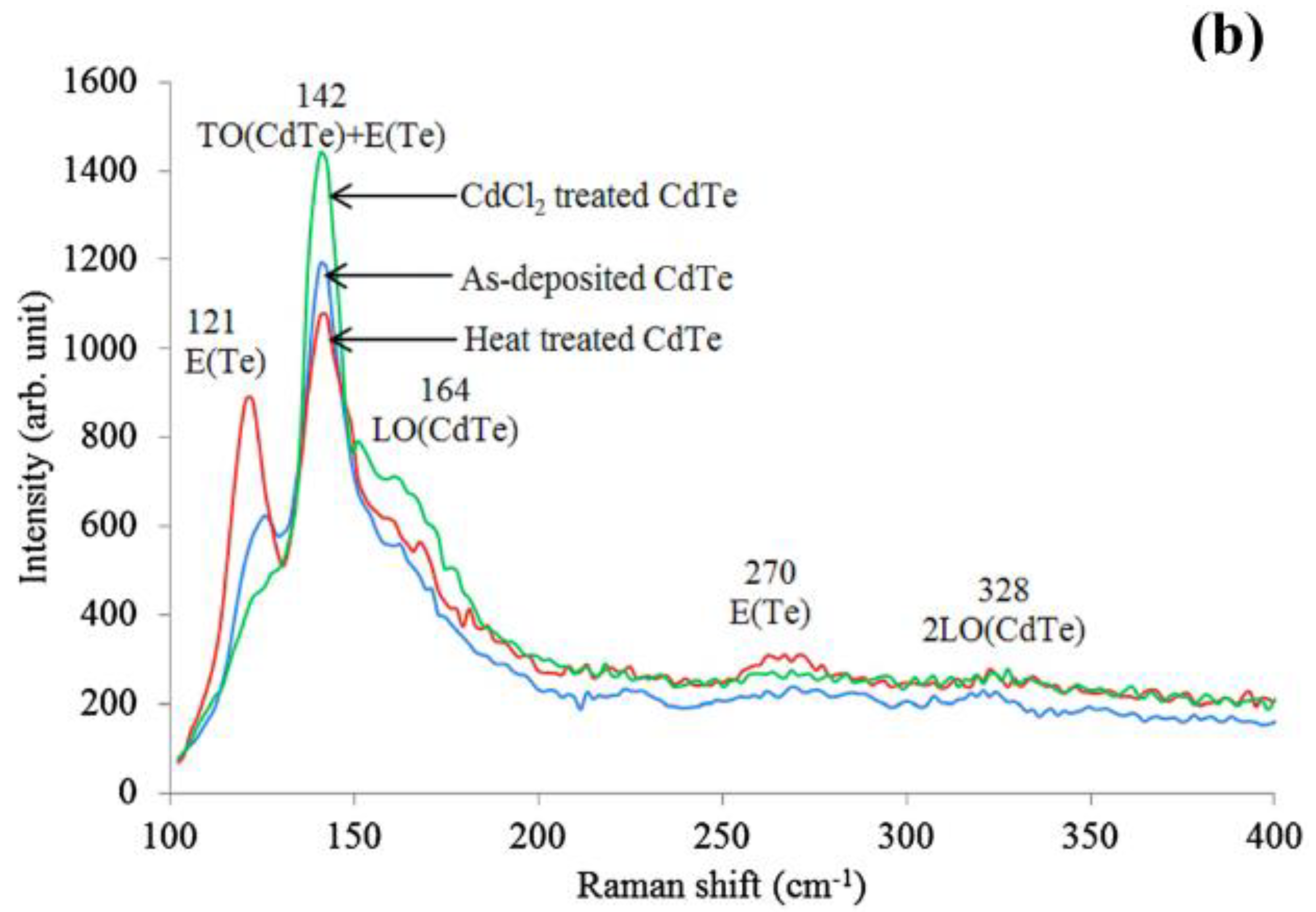
drastically reduces mid-bandgap defects in CdTe, reducing charge carrier recombination (see PL results in Section 2.3);
(iv). 
activates grain boundaries, minimises charge-carrier recombination and contributes positively towards PV performance (see Section 2.7).

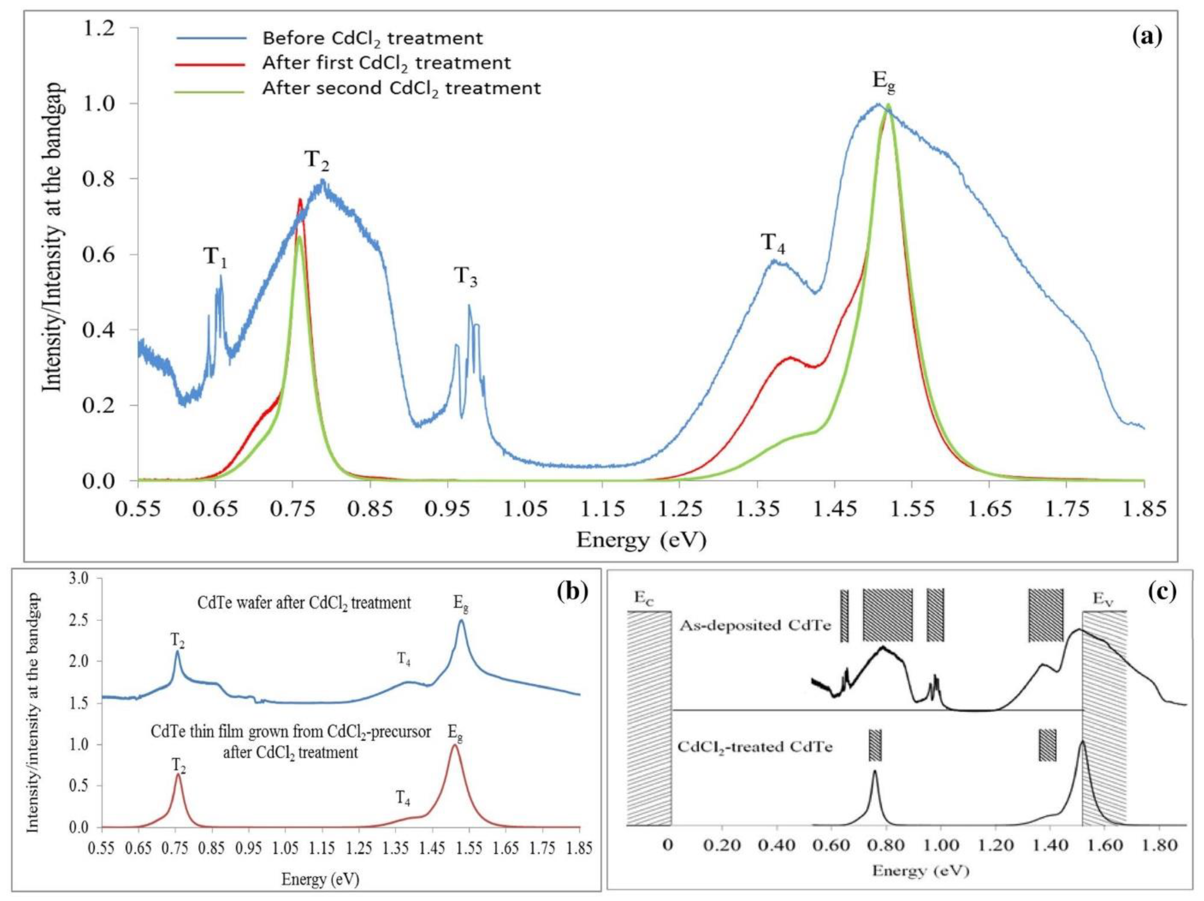
2.3. Low Concentration of Mid-Gap Defects in Cd-Rich CdTe when Compared to Te-Rich CdTe

2.3.1. PL from Single Crystal Surfaces

It is highly relevant to summarise the results reported in two articles published in the 1980s on chemically etched CdTe single crystals [23,24]. Paper [23] described how Te-rich and Cd-rich CdTe surfaces can be produced by etching in acidic and alkaline solutions, respectively. The Schottky diodes prepared by the deposit of Au or Sb contacts produced good rectifying contacts on both surfaces. Te-rich surfaces produced Schottky barriers ~0.73 eV, with over ~106 rectification factors (RF = IF/IR) indicating the Fermi level pinning at the mid-gap. Cd-rich surfaces produced superior Schottky diodes with over ~109 rectification factors and barrier heights of ~0.93 eV, indicating the Fermi level pinning closer to the valence band edge. This work was highly reproducible and consistent, and proved that the Cd-rich CdTe layers were highly suitable for making excellent rectifying contacts with high potential barrier heights.
Our earlier work [24] has reported the PL results obtained from the above two surfaces. These spectra showed the existence of mid-gap defects in Te-rich CdTe surfaces. When the surfaces are etched to produce Cd-richness, mid-gap defect states are completely or partially removed. In addition, defect levels closer to the valence band are introduced, causing the Fermi level pinning in the vicinity of the valence band edge. Both the electrical contact work and the PL work confirm that Cd-rich CdTe surfaces are more suitable than Te-rich CdTe surfaces for electronic device fabrication.

2.3.2. PL from Electroplated CdTe Thin Films

CdTe layers have been electroplated by the solar energy group at Sheffield Hallam University using three different Cd precursors; Cd-sulphate [8,25], Cd-nitrate [26] and Cd-chloride [27]. The results have been published widely, and Figure 5a shows the PL results obtained for layers grown using Cd-chloride precursor. Note the large concentration of mid-gap defects T1, T2 and T3 for as-deposited CdTe layers [28]. In II-VI semiconductors, these are known as “Killer Centres”, and detrimental due to charge carrier recombination taking place in electronic devices like solar cells. Note also the drastic reduction in defects after CdCl2 treatment. However, even after two CdCl2 treatments, the mid-gap defects still exist within a narrower energy band.
Figure 5b also compares the PL spectra obtained for commercially available CdTe wafer after CdCl2 treatment with the ED-CdTe grown from Cd-chloride precursor. Clearly, the ED-CdTe thin layers show cleaner PL spectra, demonstrating their high electronic and optical properties. This could be due to the additional use of Cd-chloride precursor, incorporating Cl atoms or ions even during the growth of the material.
Figure 5c shows the defect distribution between Ec and Ev of CdTe material electroplated using Cd-chloride precursor. As-deposited layers are full of defects, but the CdCl2-treated layers show excellent PL spectra, indicating a reduction in defects in the band gap. If we can completely remove the defects at the mid-gap, the material will produce high-performing solar cells.
(i). 
Te-rich CdTe surfaces and thin films are full of mid-gap killer centres. The Fermi level is pinned at ~0.73 eV when devices are fabricated.
(ii). 
Cd-rich CdTe surfaces have reduced mid-gap defects and are more highly suited for fabricating electronic devices than Te-rich CdTe surfaces.
(iii). 
Cd-rich CdTe surfaces and thin films minimise mid-gap killer centres and enhance defects closer to the valence band to produce Fermi level pinning ~0.96 eV. These materials therefore minimise charge carrier recombination process in devices made on Cd-rich materials and surfaces.
(iv). 
CdCl2 treatment removes mid-gap defects and also minimises other defects within the energy band gap.

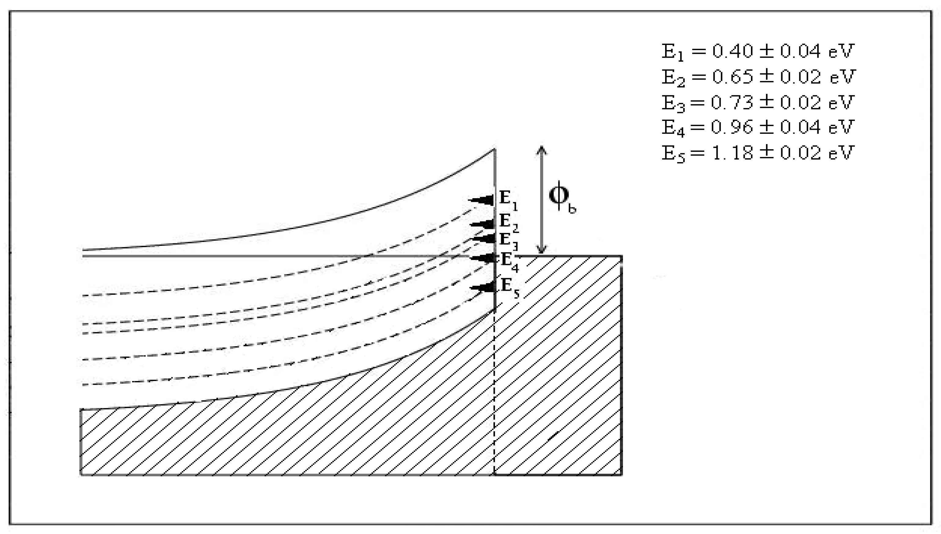
2.4. Fermi Level Pinning at n-CdTe/Metal Interface

Electrical contacts to CdTe have enormous importance in PV solar cells developed using this material. The main author’s comprehensive work on this subject on vacuum-cleaved, air-cleaved and chemically etched CdTe surfaces was reviewed in 1998 [29]. For thin-film solar cells, the results on chemically etched CdTe surfaces are highly appropriate. This work established the nature of an n-CdTe/metal interface, as shown in Figure 6 [29,30].
Electrical contacts to n-CdTe surfaces show a complex nature, with Fermi level pinning occurring at five main defect states. These five potential barriers measured using I–V technique are listed in Figure 6 with their error margins and coincide with the defect levels explored using methods like photoluminescence (PL), deep level transient spectroscopy (DLTS) and ballistic electron emission microscopy (BEEM) [29,30,31]. Fermi level pinning position depends on the nature of the material growth and the surface preparation prior to metallisation.
Pinning at E1, E2 or E3 is very common when the surface is etched to produce Te-richness. These pinnings produce discrete potential barrier heights of 0.40, 0.65 or 0.73 eV. On the other hand, Cd-rich layers pin the Fermi level at the E4 or E5 levels, producing potential barriers of 0.96 or 1.18 eV. In order to produce Schottky barriers with the highest rectification property, the Fermi level should be pinned at the E5 level. To enhance and support this Fermi level pinning, p-type dopants, such as Cu or Sb, can be added to the metal contact. These p-dopants diffuse to the top layer of n-CdTe and dope it as p+, forcing the Fermi level to approach closer to the valence band edge. Therefore, a trace of Cu and Sb in the metal contact helps to produce a large potential barrier at the interface. However, in the case of Cu, if a large number of Cu contacts or a single Cu contact is made, large numbers of Cu atoms will diffuse into the deep n-CdTe due to their small atomic size, and through self-compensation, the CdTe will become very resistive. This will in turn degrade the rectifying property by increasing the series resistance. This is the main reason to use Cu/Au or Cu/Ni electrical contacts with only a trace of Cu to produce stable rectifying contacts at the n-CdTe/metal interface. Because of the large atomic size and the strong chemical bond formation, Sb will not diffuse deeply into the n-CdTe and create detrimental effects in the manner of Cu. Sb-containing electrical contacts on n-type CdTe show stable electrical properties.
(i). 
To form good rectifying contacts with large Schottky barriers at n-CdTe/metal interface, a Cd-rich CdTe surface should be used.
(ii). 
To help and support the Fermi level pinning closer to the valence band, a trace of p-dopant, such as Cu or Sb in the metal contact can be used. Large amounts of Cu, however, will diffuse into the n-CdTe layer and increase the series resistance via self-compensation, degrading the device.

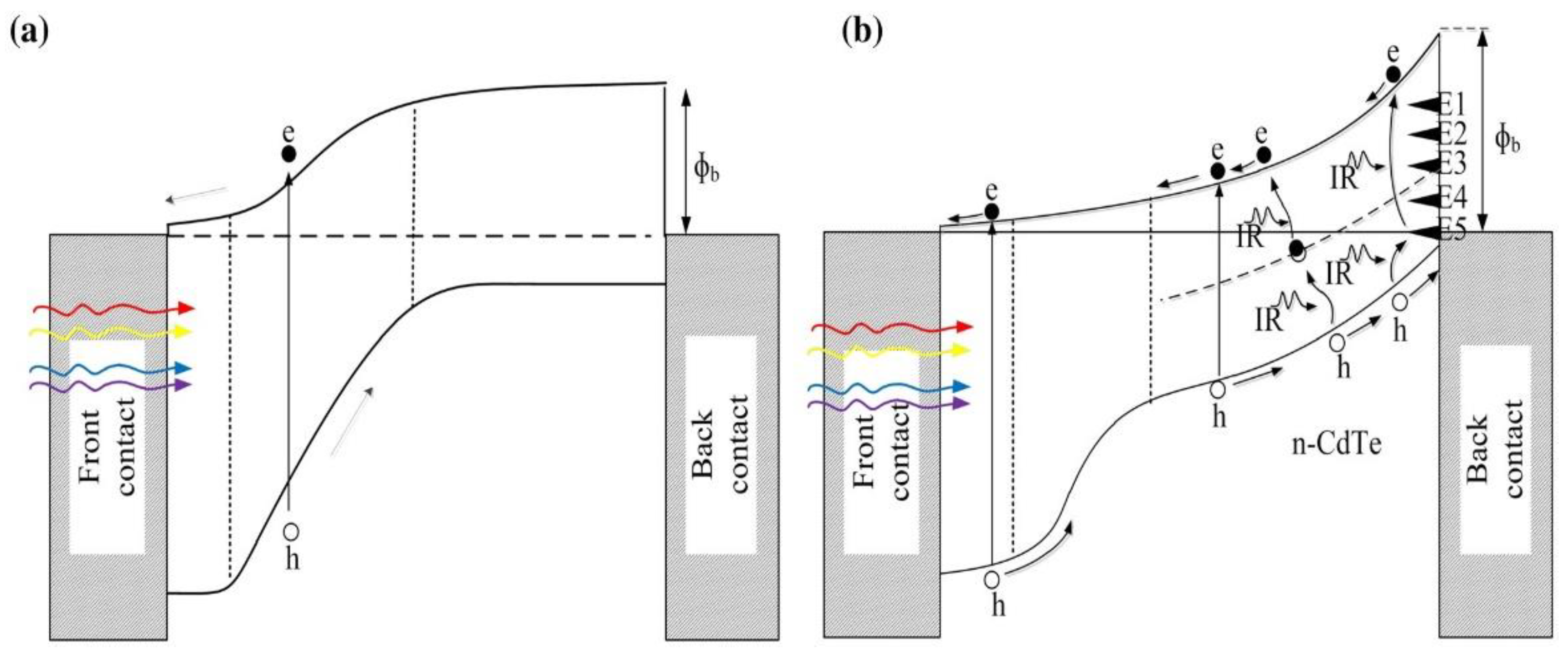
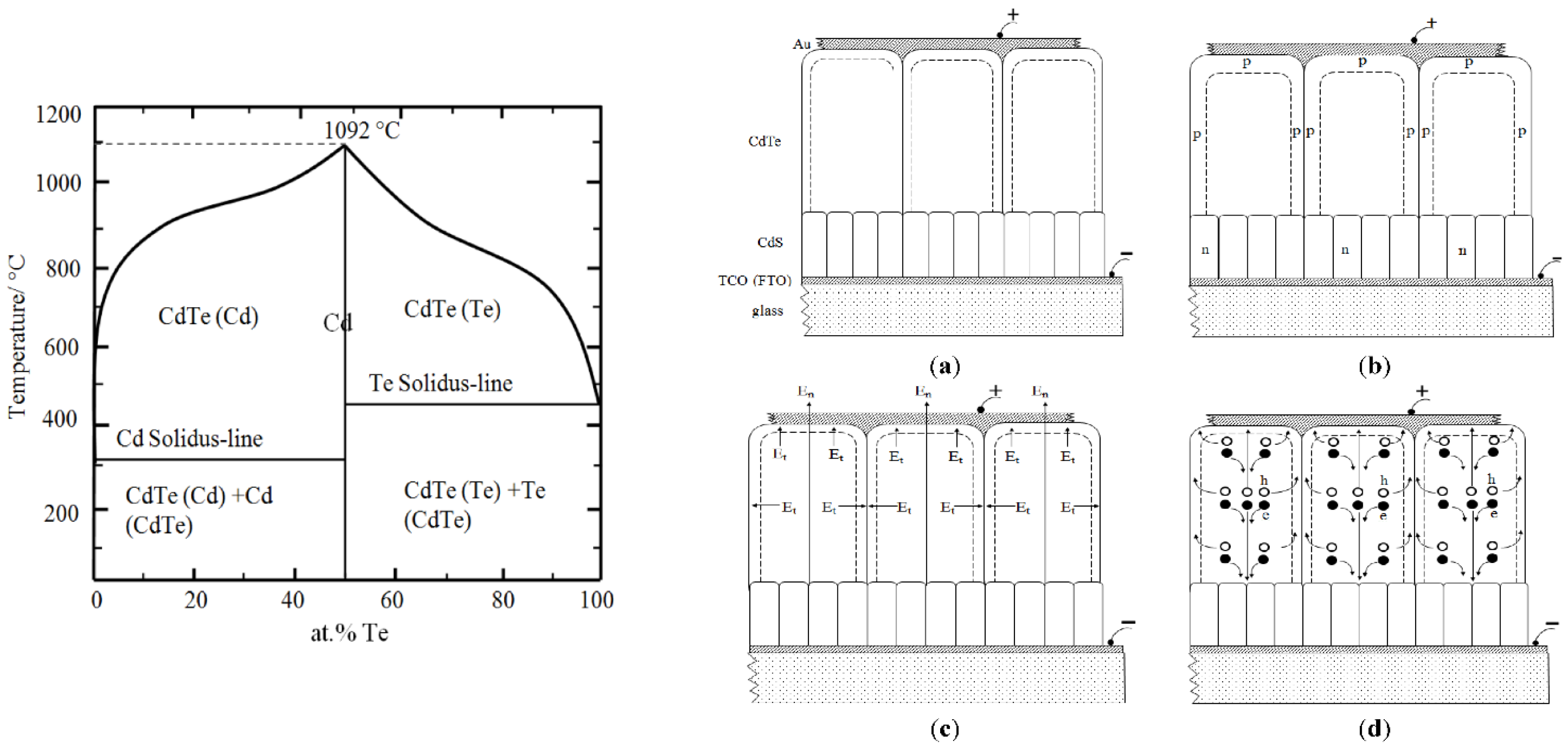
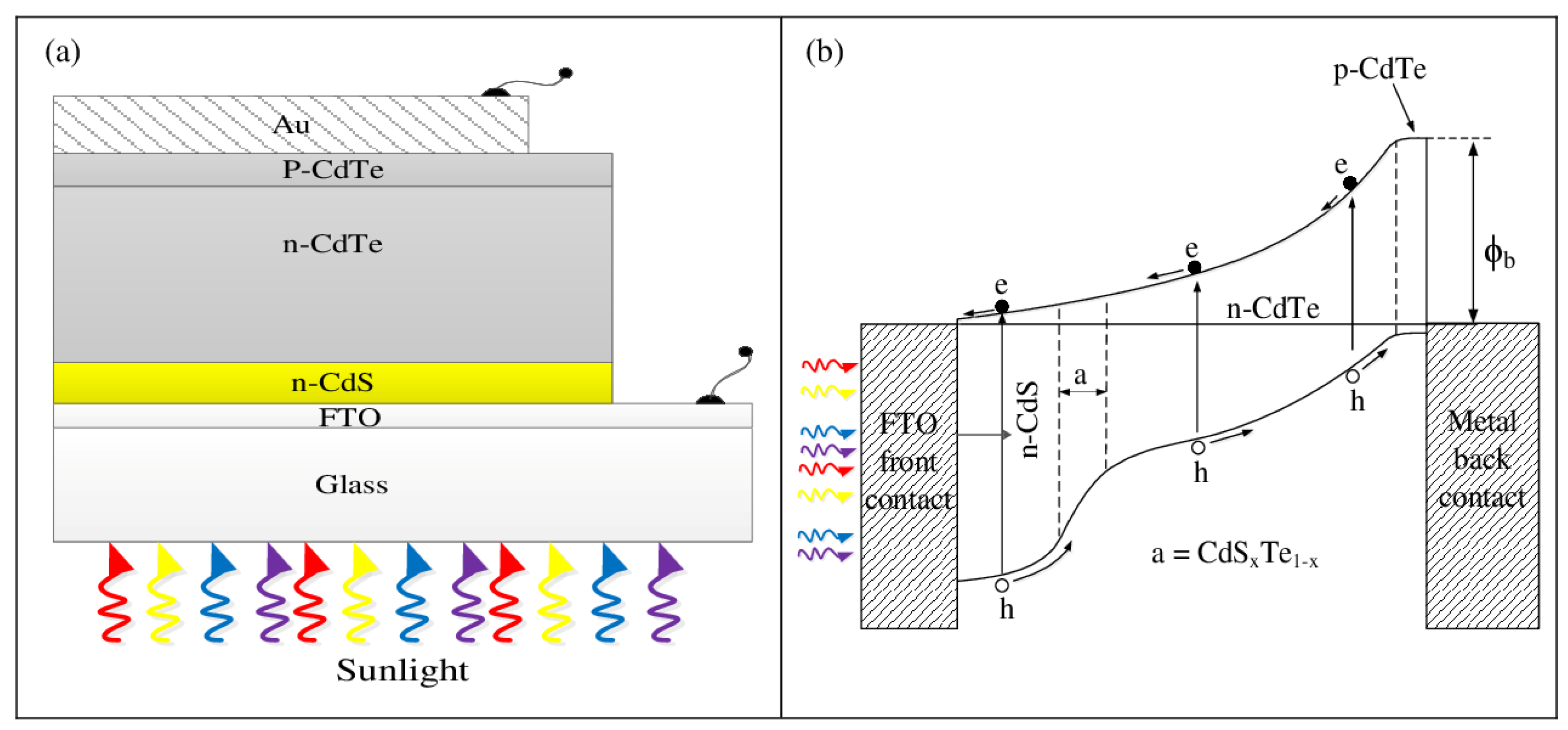
2.5. Two Possible Device Configurations for CdS/CdTe Structure

It is now obvious that there are two possible device configurations for CdS/CdTe structures [6,7]. The CdS window material is always n-type in electrical conduction due to its native defects, but the CdTe can easily exist in both p-type and n-type electrical conduction. Depending on the growth conditions used, the material can have different compositions, and hence it could be p- or n-type, depending on whether the method produces Te-rich or Cd-rich material layers, respectively.
If the CdTe grown is p-type, then the CdS/CdTe structure forms a genuine n-p junction, and the back electrical contact should be a low-resistance ohmic contact (see Figure 7a). Addition of Cu to the electrical contact makes the top layer p+, reducing the contact resistance and improving the initial device performance. Further Cu diffusion into the p-CdTe should not degrade the device performance, since the p-CdTe layers are doped with a p-dopant. The CdS/CdTe interface will merge during the growth and processing, reducing interface states and creating a gradual bandgap variation from 2.42 eV to 1.45 eV.
When the CdTe grown is n-type, the situation is very different. Because of the bandgap difference between CdS and CdTe, a weak but rectifying n-n hetero-junction forms. At higher-temperature growth and processing, intermixing at the interface takes place, removing interface states and producing a graded bandgap closer to the interface. If the processing is completed so that the Fermi level is pinned at the E5 level, a very large Schottky barrier of 1.18 eV can be formed at the back contact. It should be noted that this Schottky barrier height is similar to or larger than that of a potential barrier of n-p junction formed at CdS/CdTe structure. There are then two rectifying contacts in this structure supporting each other during the PV process (see Figure 7b). The photo-generated currents from two junctions add up, and therefore these two rectifying contacts are connected in parallel. In fact, the device is a tandem solar cell and should perform much better than the single n-p junction solar cell. In this case, traces of Cu in the back metal contact enhance the initial performance of the device, but Cu diffusion into the deeper n-CdTe degrades the device with time. This effect has been experimentally observed and reported on many occasions [31,32,33,34], and is excellent evidence that the CdTe material used in high performing solar cells is n-type in nature.
(i). 
When the CdTe is grown as a p-type (Te-rich) material, the device is a simple n-p junction. The back electrical contact should be a low-resistance ohmic contact.
(ii). 
When the CdTe is grown as an n-type (Cd-rich) material, the device is a combination of n-n hetero-junction combined with a large Schottky barrier at the back. These two rectifying interfaces support each other, and therefore should perform better than the single n-p junction.

2.6. Achieving Better Performance from n-CdS/n-CdTe Structures

The above discussion clearly suggests that both p-CdTe and n-CdTe materials are capable of forming PV active devices, but the n-CdTe forms superior solar cells. What remains is to conduct an experiment to test this idea. We carried out these experiments using electroplated CdTe material, and the results are shown in Figure 8 [34].
As discussed in Section 2.1, a CdTe electrolyte was prepared, and CdTe layers were grown on glass/FTO substrates at different voltages. PEC measurements were carried out to determine the Vi, the conversion voltage from p-CdTe to n-CdTe. For this particular bath, the Vi was 1368 mV. The PEC curve obtained for the CdCl2-treated layers is presented in all five panels in Figure 8 in red colour. The intensity of the dominant (111) XRD peak shown in the first panel indicates that the highest crystallinity was obtained closer to the Vi on the Cd-rich side. The devices made in an identical way with the Au contacts were measured, and device parameters were plotted separately against Vg in the other four panels. It is clear that both p-CdTe and n-CdTe produced PV-active devices, but the Cd-rich CdTe layers grown at voltages greater than Vi showed superior device parameters. Although the highest efficiency observed for this experiment was ~7%, the results confirmed that the arguments presented in Section 2.5 are valid. The resultant efficiency values depended on various factors, such as the purity of the electrolyte and the processing steps. Repeated experiments showed similar results, confirming the above predictions.
(i). 
All four solar cell parameters, Voc, Jsc, FF and efficiency produced by glass/FTO/n-CdS/n-CdTe/Au structures were better than those produced by glass/FTO/n-CdS/p-CdTe/Au structures.
(ii). 
Therefore, in order to develop high efficiency solar cells, Cd-rich n-CdTe should be used rather than Te-rich p-CdTe material.

2.7. Activation of Grain Boundaries by CdCl2 Treatment to Positively Contribute to the PV Effect

As described in Section 2.2, CdCl2 treatment improves the stoichiometry of CdTe, removing any precipitated and excess Te in the layers, improving crystallinity, and drastically reducing mid-gap killer centres. In addition, another important process takes place by activating grain boundaries to positively contribute to the PV action.
To discuss this process, it is important to observe the phase diagram of CdTe material, as shown in Figure 9 [35]. The melting point (MPt) of stoichiometric and pure CdTe is 1092 °C. It is a well-known phenomenon in physical chemistry that the melting point drastically reduces when impurities are added to any pure material. It is clear from the phase diagram that when CdTe has excess Te or Cd, the melting point reduces to ~(450–600) °C. During the CdCl2 treatment in air, additional impurities, such as excess Cd, Cl and O2, are added to the system. Accumulation of many other impurities, especially in grain boundaries, are possible during any growth technique. Due to these impurities in CdTe, the MPt of grain boundary materials can reduce even below 450 °C, reaching the heat treatment temperatures used during CdCl2 treatment.
In order to discuss the microscopic activities taking place during CdCl2 heat treatment, let us consider the CdS/CdTe structure with columnar-grown materials. It is well known that low-temperature semiconductor growth techniques produce columnar type materials, and in the case of CdTe, the grains are usually extended from the front to the back of the thin-film structure. For ease of discussion, the ideal situation is drawn in Figure 9a–d. Before completing the back electrical contact, CdCl2 is deposited on the CdTe surface in numerous ways as discussed earlier, dried and heat treated in air at ~420 °C for about 20 min. During this time, pure CdTe crystals (n-type in Figure 9a presentation) remain as a solid, since their MPt is ~1092 °C. However, the grain boundary material is full of impurities (excess Cd and Cl from CdCl2, O from air and any other impurities introduced during the growth). Therefore, this material begins melting along the grain boundaries at lower temperatures, including at the CdS/CdTe interface. Due to convection currents, all impurities freely move around, uniformly distributing along grain boundaries, and some volatile impurities can escape from the system. The exact melting temperature has been identified as 385 ± 5 °C, and at this point all solid CdTe grains freely float in thin liquid skins along grain boundaries [8]. This limited movement of CdTe grains can suddenly change the orientation and show a collapse of the dominant (111) XRD peak observed for the as-deposited material. After reaching the critical temperature, during heat treatment and cooled down, other strong XRD peaks {(220) and (311)} in addition to (111) peak, appear.
When the heat treatment is stopped after 20 min, the grain boundary material solidifies and forms a semiconductor with a different doping concentration to that of the solid and pure CdTe crystal. This doping concentration difference produces a transverse band bending or transverse internal electric fields along the grain boundaries. This is shown in Figure 9b,c for the case of n-CdTe crystal and p-type grain boundary material. As a result, there are weak transverse electric fields across grain boundaries in addition to the main solar cell electric field En created by the CdS/CdTe interface. Because of the effect of the two electric fields, the photo-generated charge carriers are separated and travel along the CdTe crystal and the grain boundaries (see Figure 9d). This charge carrier separation drastically reduces the recombination of e-h pairs as they traverse the device.
In the PV effect, the number of photo-generated electrons and holes are equal. In Figure 9d, the holes are moving towards the Au contact through the grain boundaries with a small cross section. An equal number of electrons, on the other hand, flows to the FTO contact through CdTe crystals with a much larger cross section. Therefore, the photo-generated current density through the grain boundaries is much higher than that through the CdTe crystals. For this reason, the cross-section electron-beam-induced current (EBIC) results must exhibit brighter grain boundaries during PV action. This has been experimentally demonstrated by two recent papers [36,37].
Another consistent observation of this material is as follows. The Te-rich material tends to produce much larger grains with (111) preferred orientation. However, the material rich in Cd tends to produce comparatively smaller grains showing numerous peaks {(111), (220), (311), etc.} in their XRD spectra. After CdCl2 treatment, the collapse of the (111) peak and the appearance of other peaks indicate that the material has moved from Te-richness to Cd-richness, as described in Section 2.2. Improved solar cells are always produced when these CdCl2-treated, Cd-rich, CdTe material layers are used.
(i). 
Columnar type or rod-type materials in thin-film solar cells are more suitable for the development of high-efficiency solar cells.
(ii). 
CdCl2 treatment activate grain boundaries, minimise charge-carrier recombination and contribute positively to improving PV performance.

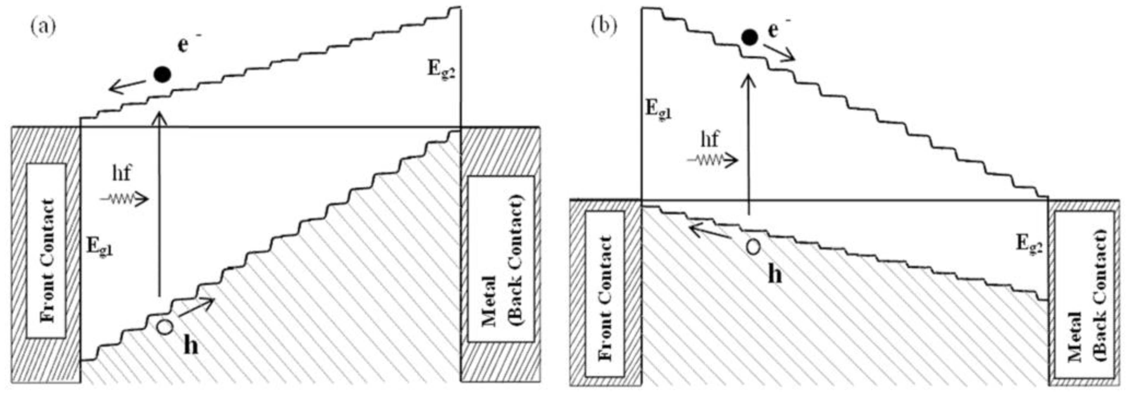
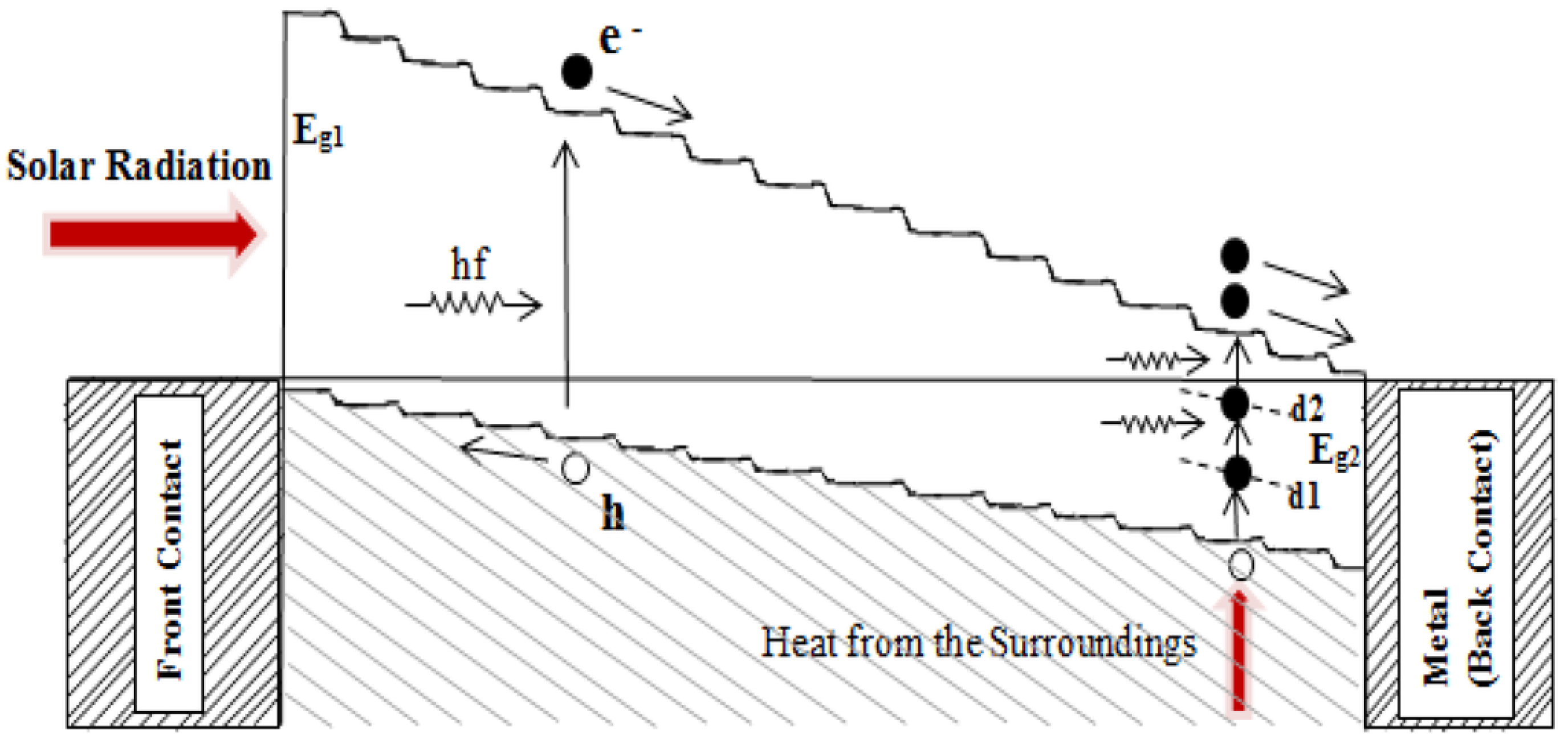
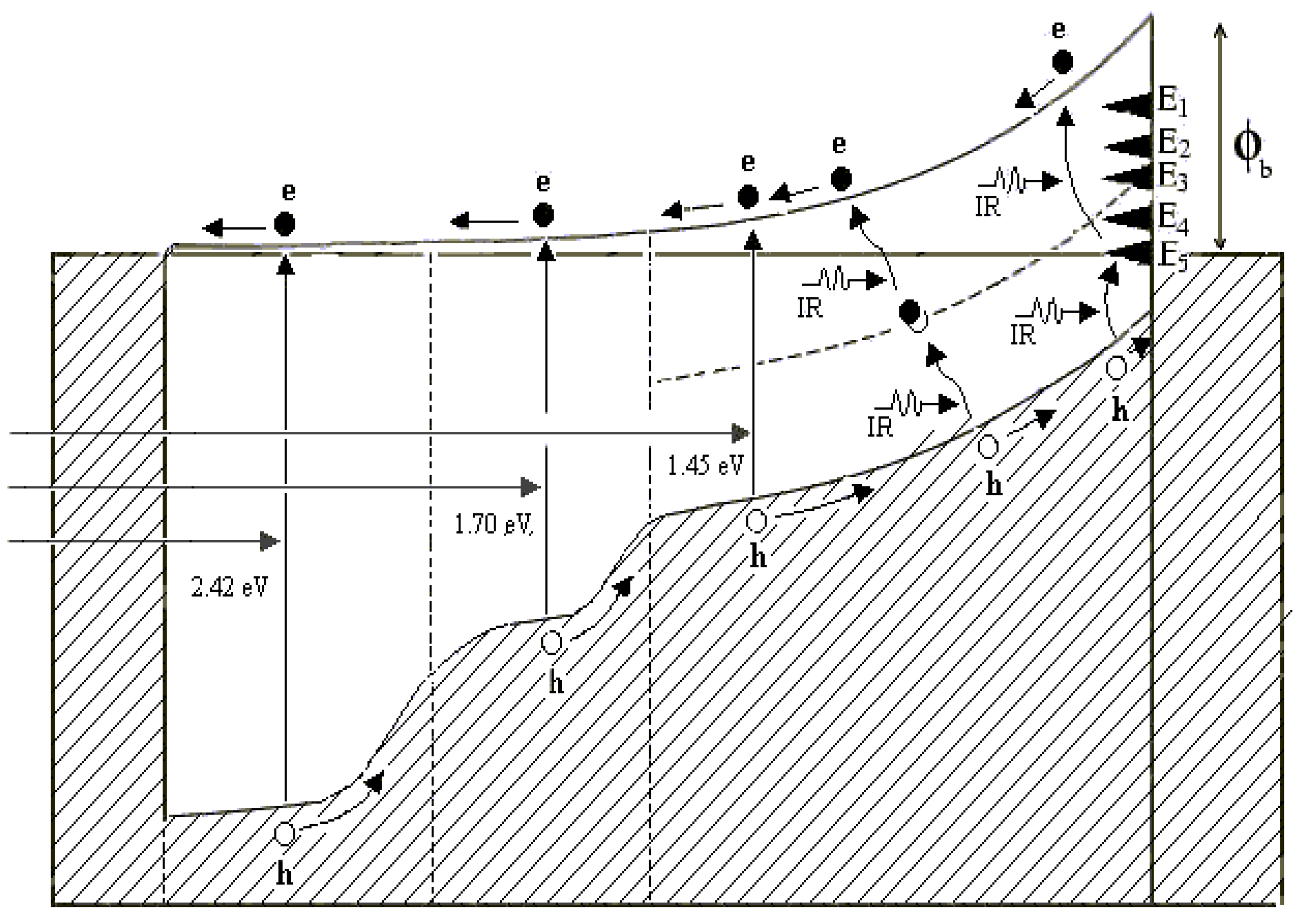
2.8. Graded Bandgap Multilayer Devices for Effective Harvesting of All Photons

The aim of PV devices is to harvest all photons available, if possible, to achieve high-performing solar cells. The Solar Energy Group at Sheffield Hallam University designed a graded bandgap multilayer solar cell to develop such a device [7,38,39,40]. By expanding the energy band diagram of Figure 7b, the graded band gap structure shown in Figure 10a was designed using n-type window material. Similar devices can be designed on p-type window material, as shown in Figure 10b. The Voc of both these designs depends on the smallest energy band gap (Eg2) used in the device. Therefore, to achieve Voc values above 1.00 V, the Eg2 value should be kept ~1.30 eV. Out of these two designs, the one built on p-type window material has more advantages. Because of the much larger bandgap of the window material (Eg1), the slope of the conduction band can be increased. This means that the internal electric field throughout the device can be kept high for charge carrier separation and collection. The other advantage is for increased impact ionisation. When the electrons created at the front accelerate towards the back contact, the band gap gradually reduces. Therefore, the accelerated electrons gain adequate energy to create e-h pairs in small band gap materials available towards the back of the device.
The above designs used all possible solid-state principles to absorb UV, visible and infra-red radiations through the use of graded band gap material layers. Furthermore, the impact ionisation and impurity PV effect were incorporated into these devices to enhance the short circuit current density. Once the concept had been established, the next stage was to experimentally test these theoretical ideas.
We experimentally tested the device designed on p-type window material [39]. N-type GaAs wafers were used as the substrate, keeping Eg2 at 1.43 eV. Then, the most studied GaAlAs alloy was deposited by metal organic chemical vapour deposition (MOCVD) method, by increasing the Al concentration gradually towards the front of the device. This Al increase was continued until the front layer band gap reached ~2.20 eV (Eg1). The layers close to the GaAs substrate were n-doped with Si, and the Si concentration was gradually reduced towards the middle of the structure. Then, the layers towards the front were gradually grown with p-type doping with carbon. The total thickness of the graded band gap structure was set to ~3.0 µm (see Figure 11a). Solar cells were processed by making ohmic contacts to both the front, and the back n-GaAs substrate. Front contacts were made using grid-type contacts to reduce shading, and three different-sized devices were made as shown in Figure 11b.
These devices were assessed for their device performance under AM1.5 standard conditions. As we expected, excellent device parameters were observed as Voc~1.115 V, Jsc~12 mA cm−2, FF~0.86 and efficiency ~12% [39,40]. These measurements were independently verified by measuring in PV labs at South Bank University, Switzerland, Michael Gratzel’s group and NREL in the US. During the second growth, the doping concentration at the rear of the device was optimised, the Jsc increased to ~24 mA cm−2 and the conversion efficiency increased to ~19% [32,33]. Experimental testing with a well-known material confirms the validity of this new design, and the aim is then to produce these devices using low-cost, scalable and manufacturable techniques.
Since the impurity PV effect was expected from this device, an experiment was performed to check the existence of this effect. Devices were mounted in a completely dark cryostat, and their I-V characteristics were measured. Unexpectedly, these devices produced Voc values in the range of 750–900 mV in complete darkness [41]. As shown in Figure 12, these devices had two inputs under illumination, but the main input of sunlight was cut off when they were mounted in complete darkness. However, the device was surrounded by IR radiation, and this radiation created e-h pairs using multistep electron promotion via impurity levels in the semiconductor. Usually, the impurity levels in solar cells reduce performance due to recombination via impurity levels. However, in these devices, the impurity levels were kept within a strong internal electric field. When this happens, the first electron excitation from the valence band to an impurity level creates a hole in the valence band. This hole is rapidly taken away to the front contact by the strong electric field, and therefore the electron trapped in the impurity level cannot relax and neutralise. The next possibility is the promotion of this electron by another IR photon to the next higher impurity level. As this process is repeated, holes and free electrons are created in the valence band and the conduction band, respectively. Excellent band bending present in the device accumulates holes in the front contact and electrons in the back contact, producing very high Voc values in complete darkness [41]. We also performed IPCE experiments, and some devices showed up to 140% IPCE signal, confirming the presence of impact ionisation in these devices [33].
To develop low-cost devices using electroplating, it is essential to develop p-type window materials first. While current efforts are focused on this line [42,43], initial graded band gap devices have been attempted on the already available n-type window materials. Figure 13 shows one such device. Even with three layers and limited band gap grading, 15.3% efficiency has been achieved [44].
(i). 
Graded band gap devices can be produced on both n-type and p-type window materials, incorporating contributions from impact ionisation and the impurity PV effect.
(ii). 
These devices can absorb more photons in UV, visible and IR regions of the sun’s spectrum and make use of IR radiation from the surroundings.
(iii). 
Since the concept is experimentally proven with impressive cell parameters, future efforts should be focused on the development of next-generation high-efficiency graded band gap solar cells based on p-type window layer, using low-cost, scalable and manufacturable techniques.

3. The Ways Forward

All the results presented above on the materials and device issues around CdS/CdTe were studied using the electroplated CdTe. In this comprehensive programme, the highest efficiencies observed for lab-scale small devices were in the range 15–18% [31,44]. One of the main reasons for this was the growth of CdTe at very low temperature ~85 °C. When semiconductors are grown at low temperatures, materials can have large concentrations of native defects, and are not suitable for device applications. However, post-growth heat treatment ~420 °C in the presence of CdCl2 converts this material into highly crystalline material with low defects for fabricating PV active devices. This material has passed through the scale-up and commercialisation process in the manufacture of ~11% efficient ~1.0 m2 solar panels [1].
The second CdTe growth technique focused on in this article was the CSS method, which is a high-temperature semiconductor growth technique. Obviously, the crystallinity of the material is better with a low number of grain boundaries and a low concentration of native defects. This material has produced a record efficiency of 22.1%, and large area modules with efficiencies in the range 17–18% [5]. During the past six years, this conversion efficiency has not increased further. Therefore, to surpass the highest reported efficiency, it is worth critically examining the CSS growth technique with the accumulated knowledge on CdTe and CdS/CdTe devices as described above. The next sections focus on areas that can be improved using CSS growth technique.

3.1. Modify CSS Method for Producing n-CdTe Material

First of all, it is important to observe the main features of the CSS growth technique used for CdTe growth. In this method, the solid is converted into a vapour from the source at high temperature and allowed to condense on the substrate heated to a lower temperature. This technique uses a source material CdTe in the form of chunks, powder or solid target. The CdTe source is placed in a suitable boat and heated to ~565–625 °C, producing CdTe vapour. A heated substrate in the temperature range 550–620 °C is held at a close distance, typically around 2 mm, and due to the sublimation/condensation process, CdTe layer deposits on the substrate. The chamber between the source and the substrate is filled with an inert gas, such as Ar, to minimise oxidation. The deposited material layer is typically ~3-5 µm thick and can be grown in about 10 min.
The materials grown at high temperatures of 550–620 °C must have high crystallinity and low native defects. However, the overall electrical and optical properties of the layers depend on (i) the temperature of the source material and the substrate used, (ii) the pressure and the nature of the chamber environment, (iii) the composition of the source material used, and (iv) the post-growth annealing conditions. These parameters can vary from laboratory to laboratory, and therefore the solar cell conversion efficiency can also vary widely.
Observations of the published literature clearly show this wide variation in conversion efficiency reported for CSS-grown CdTe material. The groups working with this growth technique use different temperatures for the source and the substrate in the above temperature ranges, and have published a large number of papers on the materials and devices. For the purposes of this discussion, only a limited number of papers reporting solar cell efficiencies were reviewed in detail. The cell efficiencies vary widely, with ~8% [45], 12.6% [46], 15.3% [47], 15.8% [48], 16% [2] and 22.1% [5] reported in the literature. It is important to critically analyse why this wide variation is observed for the CdTe material grown by the same method or by modified CSS method.
This method creates a vapour (a mixture of CdTe, Cd and Te) from solid material through sublimation at a high temperature, which is then allowed to condense on the substrate at a lower temperature. Ideally, the sublimation and the condensation process should take place congruently, but this is not possible due to the differences in the vapour pressure of the two elements, Cd and Te. If all the CdTe molecules vaporised from the source and condensed on the substrate, the situation would be simple without any complications. However, at elevated temperature, CdTe molecules break down and Cd, Te or Te2 form in the vapour. At this point, the vapour pressures of two elements are extremely important. Published literature reports a higher vapour pressure for Te than Cd [49], and this creates complications. More Te vapour pressure means more condensation of Te on the substrate, producing Te-rich p-type CdTe. Therefore, the CSS-grown CdTe will be intrinsically Te-rich and p-type in electrical conduction. Khan et al. (2009) deposited an additional Cd layer on top of conventional CSS-grown CdTe, and found that the composition of the film changes, and the electrical conductivity changes from p-type to n-type with the increment in Cd composition [10]. However, this study did not report any device preparation, and hence the effect of Cd/Te composition on the cell performance could not be evaluated. Evani (2017) attempted to investigate the effect of Cd/Te ratio in the mixing chamber of the modified CSS- (elemental vapour transport) grown CdTe on the cell performance; however, no systemic compositional characterisation has been carried out for CdTe layers after growth [11]. Thus, not many researchers have experimentally determined and reported the composition of the grown material or the electrical conduction type of the CSS-CdTe and compared cell performance. We encountered one group reporting 74% Te presence using the XRF technique, and ~8% device efficiency for that material. It is thus very clear that the Te-rich p-type CSS-grown CdTe forms a simple p-n junction device and produces low-efficiency solar cells. Researchers normally optimise their growth conditions in order to achieve high efficiencies. From the wealth of knowledge summarised in this article, it is clear that if the CSS-CdTe can be produced reducing the excess Te in the material, the efficiency will gradually increase. To achieve higher efficiencies, the material should be stoichiometric and move into the Cd-rich region. Then the device will become a tandem solar cell with an n-n hetero-junction plus a large Schottky barrier at the back electrical contact. Therefore, the first way forward is to modify the CSS growth technique by adding some additional Cd vapour into the growth chamber. Adding metallic Cd into the precursor used or allowing the Cd vapour to reach the growth chamber changes the composition of the CdTe layers. A modified CSS vapour with Cd vapour is the way forward, and the growth conditions and all device processing steps need careful optimisation.

3.2. Improve Material Layers Further and Activate Grain Boundaries to Positively Contribute to PV Effect

All CSS-grown CdTe layers at high temperatures showed large grains a few microns wide. Most of these extended across the whole device thickness, showing columnar growth. As discussed in Section 2.7, activation of grain boundaries for the purpose of obtaining their positive contribution to device performance is essential. CdCl2 heat treatment further improves crystallinity, but this is not a drastic change as in electroplated CdTe. Electroplated as-deposited material has very small crystals ~20–65 nm in size, and after CdCl2 treatment, large grains a few microns wide are formed. In the case of CSS-CdTe, the majority of grains are already in the micron size range, but smaller grains in between them coalesce to increase the size of the grains, thus reducing grain boundaries. Therefore, XRD patterns will show some minor improvements, but the activation of grain boundaries is essential to improve device performance.

3.3. Improve the Device by Adding Se to the Front of the Device

As we first published in 2002 [31], the device can be improved by incorporating an additional layer of CdSe after CdS (see Figure 14). However, the gradual addition of Se into the CdTe layer at the front improves the grading of the band gap and the reduction in the interface states in the vicinity of CdS/CdTe hetero-junction. This takes the device towards a graded band gap solar cell, as described in Section 2.8. Once again, the introduction of Se can be achieved in a modified CSS system with vapour transport.

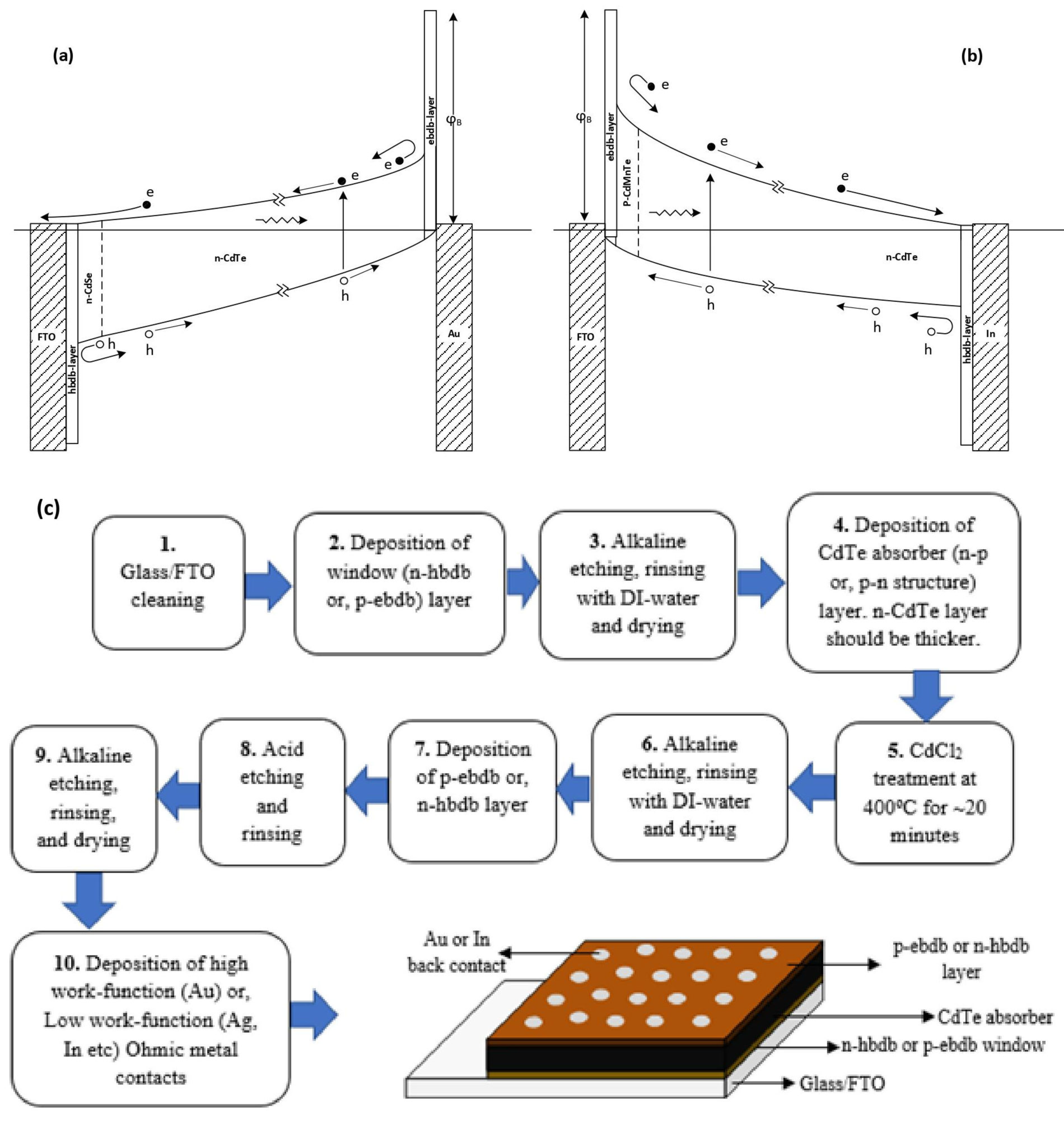
3.4. Improve Device by Adding ebdb and hbdb Layers to the Solar Cell Structure

As shown in Figure 15a,b, the device efficiency can be improved by adding electron back diffusion barrier (ebdb) and hole back diffusion barrier (hbdb) layers. By selecting a thin n+ layer for the hbdb layer and a p+ layer for the ebdb layer, the addition of series resistance can be minimised. In between these two layers, a PV active absorbing material, such as perovskite or any other rectifying (p-n, p-i-n, hetero-junction or graded band gap) structures, could be included. These two layers will prevent photo-generated electrons and holes from moving in the wrong directions, mainly resulting in an increased Voc. In the literature, the ebdb layer is known as the hole transport layer, and the hbdb layer is known as the electron transport layer.
(i). 
Because of the higher vapour pressure of Te, CSS-CdTe is intrinsically Te-rich, is p-type in electrical conduction and produces comparatively lower efficiencies. To produce Cd-rich, n-CdTe and hence high efficiencies, the CSS method should be modified to introduce Cd vapour transport into the growth chamber.
(ii). 
Grain boundaries are activated by CdCl2 treatment to positively contribute to the PV action.
(iii). 
The band gap at the front of the solar cell is graded by the addition of elements such as Se to improve PV activity of the device.
(iv). 
Suitable ebdb and hbdb layers are added to guide the direction of charge carrier flow in PV solar cells.

4. Conclusions

This review article summarised the key science surrounding the use of electroplated and CSS-grown CdTe, as well as the device issues related to CdTe-based solar cells. Based on the review of results previously reported in the literature, the path forward to achieve or even surpass the record efficiency of 22.1% using CSS-grown CdTe is suggested.
Electroplating of CdTe demonstrated that this material can be intrinsically doped by simply varying the composition. Te-rich CdTe material is p-type, and Cd-rich material is n-type in electrical conduction. Material grown at low temperature ~85 °C consisted of small crystallites in the range 20–65 nm and was full of defects, but CdCl2 treatment showed a drastic improvement, producing large crystalline grains of a few microns in size as well as reducing defects, and activating grain boundaries to positively contribute to the PV effect.
Electrical contacts on n-CdTe showed a complex situation at the n-CdTe/metal interface. Fermi level pinning produced low Schottky barriers on Te-rich material and large Schottky barriers on Cd-rich CdTe material. This observation led to the identification of an alternative device configuration for CdS/CdTe solar cell, when the CdTe layer was Cd-rich and n-type in electrical conduction, in addition to the simple p-n junction formed when Te-rich p-type CdTe was used. Experimental work showed that devices made with n-CdTe were superior to those made with p-CdTe.
The alternative device configuration with an n-n hetero-junction combined with a large Schottky barrier at the back metal contact led to the design of a graded band gap solar cell with many layers. Two types of graded band gap devices are possible based on n-type window materials and p-type window materials. The latter device has more advantages in creating a high internal electric field, and incorporation of both impact ionisation and impurity PV effects. This device design was experimentally tested with a well-researched GaAs/AlGaAs system and impressive, independently verified device parameters (Voc~1.115 V and FF~0.86) were observed.
Drawing on these scientific results observed over the past four decades, the way forward for the CSS-CdTe growth route to achieve or surpass the highest recorded 22.1% efficiency for CdTe-based solar cells are proposed. The CSS-CdTe growth technique is a high-temperature growth method and is therefore capable of producing good materials with large grains, and hence producing high efficiency devices. The five different ways suggested are: (i) modify the CSS growth system to produce Cd-rich n-CdTe material instead of producing Te-rich p-CdTe, (ii) heat treat with CdCl2 to improve the layers further and activate the grain boundaries in columnar type crystals usually obtained within the layers, (iii) grade the band gap in the front of the device using Se or any other suitable element to improve the PV effect, (iv) fabricate the devices based on p-type window layers if possible for enhanced Voc & Jsc, and (v) add an ebdb layer and a hbdb layer on both sides to enhance the Voc and hence all other parameters.
Finally, the readers’ attention is directed to a recent paper published in 2015 by the NREL group in the United States [50]. This paper states “Combining theoretical calculations and experimental measurements, we find that for both intrinsic CdTe and CdTe solar cell devices, longer minority-carrier lifetimes can be achieved under Cd-rich conditions, in contrast to the previous belief that Te-rich conditions are more beneficial”. From the evidence presented in this review article, it is clear that Cd-rich, n-type CdTe produces superior solar cells based on CdTe material. The PV community has been developing window materials to replace CdS, and the use of improved such window materials can also enhance the efficiency of these devices. By combining these new ideas, it is possible to surpass the record efficiency of 22.1% reported in 2016.

Author Contributions

The main author reviewed the four decades of findings, drafted the manuscript, and carefully edited the paper. The co-author helped in collecting some key references, drawing some diagrams, editing the draft manuscript and proof reading. All authors have read and agreed to the published version of the manuscript.

Funding

This research received no external funding.

Acknowledgments

The main author would like to thank and acknowledge the contributions made by C. J. Blomfield, S. M. McGregor, A. P. Samantilleke, N. B. Chaure, Jayne Wellings, G. Muftah, D. G. Diso, A. R. Weerasinghe, P. A. Bingham, O. K. Echendu, F. Fauzi, H. I. Salim, Fijay Fausi, N. A. Abdul-Manaf, O. I. Olusola, M. L. Madugu and A. A. Ojo. The collaborating teams in Italy (Nicola Romeo and Allesio Bosio) and in the USA (Thad Druffle, Ruvini Dharmadasa, Gamini Sumanasekera and Jacek Jasinsky) are gratefully acknowledged for their contributions through PL, other experimental work and discussions on new findings. The author would also like to thank J. S. Roberts, G. Hill, A. Tiwari, D.J.L. Brémaud, H. Reehal, K. Mahanama, M. Grätzel and K. Emery for growing materials, fabricating devices and arranging independent device measurements for graded band gap devices. Although a limited number of references have been cited in this paper, the authors wishes to acknowledge and thank many scientists who contributed to this area of research over the past few decades. Gareth Roberts (late), Mike Petty, Robin Williams and Emeric Rhoderick are gratefully acknowledged for their guidance during the main author’s early stage of scientific research to develop in this field.

Conflicts of Interest

The authors declare no conflict of interest.

References

  1. Cunningham, D.; Rubcich, M.; Skinner, D. Cadmium telluride PV module manufacturing at BP Solar. Prog. Photovolt. Res. Appl. 2002, 10, 159–168. [Google Scholar] [CrossRef]
  2. Ferekides, C.S.; Marinskiy, D.; Viswanathan, V.; Tetali, B.; Palekis, V.; Selvaraj, P.; Morel, D.L. High efficiency CSS CdTe solar cells. Thin Solid Film. 2000, 361–362, 520–526. [Google Scholar] [CrossRef]
  3. Wu, X.; Keane, J.C.; Dhere, R.G.; DeHart, C.; Albin, D.S.; Duda, A.; Gessert, T.A.; Ashar, S.; Levi, D.H.; Sheldon, P. 16.5%-efficient CdS/CdTe polycrystalline thin film solar cells. In Proceedings of the 17th European Photovoltaic Solar Energy Conference, Munich, Germany, 22–26 October 2001; pp. 995–1000. [Google Scholar]
  4. Razykov, T.M.; Ferekides, C.S.; Morel, D.; Stefanakos, E.; Ullal, H.S.; Upadhyaya, H.M. Solar photovoltaic electricity: Current status and future prospects. Sol. Energy 2011, 85, 1580–1608. [Google Scholar] [CrossRef]
  5. First Solar CdTe Cell Hits 22.1% Efficiency. Available online: https://optics.org/news/7/2/29 (accessed on 15 October 2022).
  6. Dharmadasa, I.M. Advances in Thin Film Solar Cells, 2nd ed.; Pan Stanford Publishing Ltd.: Singapore, 2018. [Google Scholar]
  7. Ojo, A.A.; Cranton, W.M.; Dharmadasa, I.M. Next Generation Multilayer Graded Bandgap Solar Cells; Springer: Berlin/Heidelberg, Germany, 2018; ISBN 978-3-319-96666-3. [Google Scholar]
  8. Dharmadasa, I.M.; Bingham, P.A.; Echendu, O.K.; Salim, H.I.; Druffel, T.; Dharmadasa, R.; Sumanasekera, G.U.; Dharmasena, R.R.; Dergacheva, M.B.; Mit, K.A.; et al. Fabrication of CdS/CdTe-based thin film solar cells using an electro-chemical technique. Coatings 2014, 4, 380–415. [Google Scholar] [CrossRef]
  9. Dennison, S. Dopant and impurity effects in electrodeposited CdS/CdTe thin films for photovoltaic applications. J. Mater. Chem. 1994, 4, 41. [Google Scholar] [CrossRef]
  10. Khan, M.A.; Shah, N.A.; Ali, A.; Basharat, M.; Hannan, M.A.; Maqsood, A. Fabrication and Characterization of Cd-Enriched CdTe thin Films by Close Spaced Sublimation; Free Library by Farlex: Huntingdon Valley, PA, USA, 2009. [Google Scholar]
  11. Evani, V.K. Improving Doping and Minority Carrier Lifetime of CdTe/CdS Solar Cells by In-Situ Control of CdTe Stoichiometry. Ph.D. Thesis, University of South Florida, Tampa, FL, USA, 2017. [Google Scholar]
  12. Nakayama, N.; Matsumoto, H.; Yamaguchi, K.; Ikagami, S.; Hioki, Y. Ceramic thin film CdTe solar cell. Jan. J. Appl. Phys. 1976, 15, 2281–2282. [Google Scholar] [CrossRef]
  13. Fritsche, J.; Gunst, S.; Golusda, E.; Lejard, M.C.; Thißen, A.; Mayer, T.; Klein, A.; Wendt, R.; Gegenwart, R.; Bonnet, D.; et al. Surface analysis of CdTe thin film solar cells. Thin Solid Film. 2001, 387, 161–164. [Google Scholar] [CrossRef]
  14. Dharmadasa, I.M. Review of the CdCl2 Treatment Used in CdS/CdTe Thin Film Solar Cell Development and New Evidence towards Improved Understanding. Coatings 2014, 4, 282–307. [Google Scholar] [CrossRef] [Green Version]
  15. Compann, A.; Bhat, A. Laser-driven physical vapor deposition for thin-film CdTe solar cells. Int. J. Sol. Energy 1992, 12, 155–169. [Google Scholar] [CrossRef]
  16. Potter, M.D.G.; Halliday, D.P.; Cousin, M.; Durose, K. A study of the effects of varying cadmium chloride treatment on the luminescent properties of CdTe/CdS thin film solar cells. Thin Solid Films 2000, 361–362, 248–252. [Google Scholar] [CrossRef]
  17. Mazzamuto, S.; Vailant, L.; Bosio, A.; Romeo, N.; Armani, N.; Salviati, G. A study of the CdTe treatment with a Freon gas such as CHF2Cl. Thin Solid Film. 2008, 16, 7079–7083. [Google Scholar] [CrossRef]
  18. Jayatirtha, H.N.; Henderson, D.O.; Burger, A.; Volz, M.P. Study of tellurium precipitates in CdTe crystals. Appl. Phys. Lett. 1993, 62, 573–575. [Google Scholar] [CrossRef]
  19. Dharmadasa, I.M.; Echendu, O.K.; Fauzi, F.; Abdul-Manaf, N.A.; Olusola, O.I.; Salim, H.I.; Madugu, M.L.; Ojo, A.A. Improvement of composition of CdTe thin films during heat treatment in the presence of CdCl2. J. Mater. Sci. Mater. Electron. 2017, 28, 2343–2352. [Google Scholar] [CrossRef] [Green Version]
  20. Moutinho, H.R.; Al-Jassim, M.M.; Abufoltuh, F.A.; Levi, D.H.; Dippo, P.C.; Dhere, R.G.; Kazmerski, L.L. Studies of recrystallization of CdTe thin films after CdCl2 treatment. In Proceedings of the 26th IEEE Photovoltaic Specialists Conference (PVSC), Anaheim, CA, USA, 29 September–3 October 1997; pp. 431–434. [Google Scholar]
  21. Rami, M.; Benamar, E.; Fahoume, M.; Chraibi, F.; Ennaoui, A.M.J. Effect of heat-treatment with CdCl2 on the electrodeposited CdTe/CdS heterojunction. Condens. Matter. 2000, 3, 66–70. [Google Scholar]
  22. Schaffner, J.; Motzko, M.; Tueschen, A.; Swirschuk, A.; Schimper, H.J.; Klein, A.; Modes, T.; Zywitzki, O.; Jaegermann, W. 12% efficient CdTe/CdS thin film solar cells deposited by low-temperature close space sublimation. J. Appl. Phys. 2011, 110, 064508. [Google Scholar] [CrossRef]
  23. Dharmadasa, I.M.; Thornton, J.M.; Williams, R.H. Effects of surface treatments on Schottky barrier formation at metal/n-type CdTe contacts. Appl. Phys. Lett. 1989, 54, 137–139. [Google Scholar] [CrossRef]
  24. Sobiesierski, Z.; Dharmadasa, I.M.; Williams, R.H. Correlation of photoluminescence measurements with the composition and electronic properties of chemically etched CdTe surfaces. Appl. Phys. Lett. 1988, 53, 2623–2625. [Google Scholar] [CrossRef] [Green Version]
  25. Diso, D.G.; Fauzi, F.; Echendu, O.K.; Dharmadasa, I.M. Optimisation of CdTe Electrodeposition Voltage for Development of CdS/CdTe Solar Cells. J. Mater. Sci. Mater. Electron. 2016, 27, 12464–12472. [Google Scholar] [CrossRef]
  26. Salim, H.I.; Patel, V.; Abbas, A.; Walls, M.; Dharmadasa, I.M. Electrodeposition of CdTe thin films solar cells using nitrate precursor. J. Mater. Sci. Mater. Electron. 2015, 26, 3119–3128. [Google Scholar] [CrossRef] [Green Version]
  27. Abdul-Manaf, N.A.; Salim, H.I.; Madugu, M.L.; Olusola, O.I.; Dharmadasa, I.M. Electroplating and characterisation of Cadmium Telluride thin films using CdCl2 as the cadmium source. Energies 2015, 8, 10883–10903. [Google Scholar] [CrossRef] [Green Version]
  28. Dharmadasa, I.M.; Echendu, O.K.; Fauzi, F.; Abdul-Manaf, N.A.; Salim, H.I.; Druffel, T.; Dharmadasa, R.; Lavery, B. Effects of CdCl2 treatment on deep levels in CdTe and their implications on thin film solar cells; A comprehensive photoluminescence study. J. Mater. Sci. Mater. Electron. 2015, 26, 4571–4583. [Google Scholar] [CrossRef]
  29. Dharmadasa, I.M. Recent developments and progress on electrical contacts to CdTe, CdS and ZnSe with special reference to barrier contacts to CdTe. Prog. Cryst. Growth Charact. Mater. 1998, 36, 249–290. [Google Scholar] [CrossRef]
  30. Dharmadasa, I.M.; Blomfield, C.J.; Scott, G.C.; Coratger, R.; Ajustron, F.; Beauvillain, J. Metal/n-CdTe interfaces: A study of electrical contacts by DLTS and BEEM. Solid State Electron. 1998, 42, 595–604. [Google Scholar] [CrossRef]
  31. Dharmadasa, I.M.; Samantilleke, A.P.; Young, J.; Chaure, N.B. New ways of development of Glass/Conducting Glass/CdS/CdTe/metal thin film solar cells based on a new model. Semicond. Sci. Technol. 2002, 17, 1238–1248. [Google Scholar] [CrossRef]
  32. Dharmadasa, I.M.; Alam, A.E.; Ojo, A.A.; Echendu, O.K. Scientific complications and controversies noted in the field of CdS/CdTe thin film solar cells and the way forward for further development. J. Mater. Sci. Mater. Electron. 2019, 30, 20330–20344. [Google Scholar] [CrossRef] [Green Version]
  33. Dharmadasa, I.M.; Ojo, A.A. Unravelling complex nature of CdS/CdTe based thin film solar cells. J. Mater. Sci. Mater. Electron. 2017, 28, 16598–16617. [Google Scholar] [CrossRef] [Green Version]
  34. Dharmadasa, I.M.; Ojo, A.A.; Salim, H.I.; Dharmadasa, R. Next Generation Solar Cells Based on Graded Bandgap Device Structures Utilising Rod-type Nano-Materials. Energies 2015, 8, 5440–5458. [Google Scholar] [CrossRef] [Green Version]
  35. Zanio, K. Semiconductors and Semimetals; Academic Press: New York, NY, USA, 1978; Volume 13. [Google Scholar]
  36. Zywitzki, O.; Modes, T. High resolution EBIC investigations on cross-sections of cadmium telluride thin film solar cells. In Proceedings of the 27th European Photovoltaic Solar Energy Conference and Exhibition, Frankfurt, Germany, 24–28 September 2012; pp. 2226–2231. [Google Scholar]
  37. Luria, J.; Kutes, Y.; Moore, A.; Zhang, L.; Stach, E.A.; Huey, B.D. Charge transport in CdTe solar cells revealed by conductive tomographic atomic force microscopy. Nat. Energy 2016, 1, 16150. [Google Scholar] [CrossRef]
  38. Dharmadasa, I.M. Third Generation Multi-layer Tandem Solar Cells for Achieving High Conversion Efficiencies. Sol. Energy Mater. Sol. Cells 2005, 85, 293–300. [Google Scholar] [CrossRef]
  39. Dharmadasa, I.M.; Roberts, J.S.; Hill, G. Third Generation Multi-layer Graded Bandgap Solar Cells for Achieving High Conversion Efficiencies—II: Experimental results. Sol. Energy Mater. Sol. Cells 2005, 88, 413–422. [Google Scholar] [CrossRef]
  40. Dharmadasa, I.M.; Kalyanaratne, N.D.P.S.R.; Dharmadasa, R. Effective harvesting of photons for improvement of solar energy conversion by graded bandgap multilayer solar cells. J. Natn. Sci. Found. Sri Lanka 2013, 41, 73–80. [Google Scholar] [CrossRef]
  41. Dharmadasa, I.M.; Elsherif, O.; Tolan, G.J. Solar cells active in complete darkness Solar Cells Active in Complete Darkness. J. Phys. Conf. Ser. 2011, 286, 012041. [Google Scholar] [CrossRef]
  42. Alam, A.E.; Ojo, A.A.; Jasinski, J.; Dharmadasa, I.M. Magnesium incorporation in n-CdTe to produce wide bandgap p-type CdTe:Mg window layers. Chem. Eng. 2018, 2, 59. [Google Scholar] [CrossRef] [Green Version]
  43. Alam, A.E.; Olusola, O.I.; Loch DA, L.; Shukla, K.; Cranton, W.M.; Dharmadasa, I.M. Electrodeposition of ternary compounds for novel PV application and optimisation of electrodeposited CdMnTe thin-films. Sci. Rep. 2020, 10, 21445. [Google Scholar] [CrossRef] [PubMed]
  44. Ojo, A.A.; Dharmadasa, I.M. 15.3% efficient graded bandgap solar cells fabricated using electroplated CdS and CdTe thin films. Sol. Energy 2016, 136, 10–14. [Google Scholar] [CrossRef] [Green Version]
  45. Paulson, P.D.; Dutta, V. Study of in situ CdCl2 treatment on CSS deposited CdTe films and CdS/CdTe solar cells. Thin Solid Film. 2000, 370, 299–306. [Google Scholar] [CrossRef]
  46. Davies, A.; Sites, J.R.; Enzenroth, R.A.; Sampath, W.S.; Barth, K.L. All-CSS processing of CdS/CdTe thin-film solar cells with thin CdS layers. MRS Online Proc. Libr. 2007, 1012, 323. [Google Scholar] [CrossRef]
  47. Amin, N.; Rahman, K.S. Close-Spaced Sublimation (CSS): A Low-Cost, High-Yield Deposition System for Cadmium Telluride (CdTe). Thin Film. Sol. Cells 2017, 361. [Google Scholar] [CrossRef] [Green Version]
  48. Romeo, A.; Khrypunov, G.; Alassini, S.G.; Zogg, H.; Tiwari, A.N.; Romeo, N.; Bosio, A.; Mazzamuto, S. Comparison of CSS-CdTe and PVD-CdTe with different activation processes. In Proceedings of the 22nd European Photovoltaic Solar Energy Conference, Milan, Italy, 3–7 September 2007. [Google Scholar]
  49. Vapor Pressures of the Elements (Data Page)—Wikipedia. Available online: https://en.wikipedia.org/wiki/Vapor_pressures_of_the_elements_(data_page) (accessed on 18 October 2022).
  50. Reese, M.O.; Perkins, C.L.; Burst, J.M.; Farrell, S.; Barnes, T.M.; Johnston, S.W.; Kuciauskas, D.; Gessert, T.A.; Metzger, W.K. Intrinsic surface passivation of CdTe. J. Appl. Phys. 2015, 118, 155305. [Google Scholar] [CrossRef]
Figure 1. Basic processing steps of fabricating, and the schematic diagram of the glass/FTO/CdS/CdTe/metal PV solar cells.
Energies 15 09510 g001
Figure 2. Summary of results obtained for electroplated CdTe layers on glass/FTO substrates. Curve A shows the variation of the dominant XRD (111) peak intensity as a function of Vg. BiB’ shows the PEC signal variation, and the C-i-C’ curve indicates possible doping concentration changes. Shaded area indicates the suitable region for electroplating CdTe layers to fabricate PV active devices [8].
Energies 15 09510 g002
Figure 3. (a) XRD and (b) Raman spectra recorded for as-deposited (green), heat-treated in air (red) and CdCl2-treated (violet) CdTe layers to demonstrate the removal of excess Te during CdCl2 treatment [19].
Energies 15 09510 g003aEnergies 15 09510 g003b
Figure 4. SEM top views of as-deposited CdTe (a) and CdCl2-treated CdTe layers (b). Note the presence of small crystallites 20–65 nm in large clusters or agglomerations. (c,d) The visualisation of cross-sections based on SEM and TEM observations.
Energies 15 09510 g004
Figure 5. (a) PL spectra of as-deposited CdTe layers, grown from Cd-chloride precursor and the effects of subsequent CdCl2 treatment in two steps [28]. (b) PL spectra of bulk CdTe wafers and electroplated CdTe after CdCl2 treatment, and (c) the representation of defect distribution in as-deposited and CdCl2-treated CdTe thin films. Note the drastic removal of defects from the band gap of CdTe [28].
Energies 15 09510 g005
Figure 6. Fermi level pinning positions at n-CdTe/metal interfaces in both bulk and thin-film CdTe surfaces [29,30,31]. The potential barrier height formed remains constant, irrespective of the metal work function, with any un-reactive electrical contact material used.
Energies 15 09510 g006
Figure 7. Energy band diagrams of two possible device configurations arising from glass/FTO/CdS/CdTe/metal system due to existence of CdTe in p-type (a), or n-type (b) electrical conduction [32,33].
Energies 15 09510 g007
Figure 8. Typical variation in the PEC signal for CdCl2-treated CdTe is shown in RED in each panel to separate the p-type and n-type regions. The intensity of the dominant (111) XRD peak is shown in the first panel, indicating the best crystallinity at around Vi = 1368 mV on the Cd-rich side. The device parameters for glass/FTO/CdS/CdTe/Au solar cells fabricated with CdTe layers grown in the vicinity of the transition voltage, Vi, are shown in the other four panels. Note that all device parameters are higher when the CdTe layers are rich in Cd and n-type in electrical conduction [34].
Energies 15 09510 g008
Figure 9. Phase diagram of CdTe [35] and schematic diagram of (a) columnar-type CdS/CdTe solar cells; (b) doping effects of grains after CdCl2 treatment; (c) presence of local electric fields (Et) in addition to the main electric field (En) within the device, and (d) photo-generated charge carrier separation and collection with high current densities along grain boundaries [8].
Energies 15 09510 g009
Figure 10. Energy band diagrams of graded bandgap devices based on (a) n-type window material and (b) p-type window material. Note that the number of potential barriers achievable for electron transport is higher in devices based on p-type window materials [6,7,38].
Energies 15 09510 g010
Figure 11. (a) The schematic diagram of the graded bandgap device structure grown with AlGaAs on GaAs substrate, and (b) pictures of fully fabricated graded bandgap devices with different sizes [39].
Energies 15 09510 g011
Figure 12. Effective use of naturally occurring defects in semiconductors to create e-h pairs by multistep photon absorption. Photons with energy less than the smallest bandgap (Eg2) can be harvested using the impurity PV effect [41].
Energies 15 09510 g012
Figure 13. (a) Schematic diagram and (b) energy band diagram of the glass/FTO/n-CdS/n-CdTe/p-CdTe/Au thin-film solar cell [44].
Energies 15 09510 g013
Figure 14. The energy band diagram of the 3-layer glass/CG/CdS/CdSe/CdTe/metal solar cell with an intermediate CdSe layer. During an annealing and aging process, this structure becomes a multilayer graded bandgap tandem solar cell due to intermixing of materials at two hetero-junctions [31].
Energies 15 09510 g014
Figure 15. Main features (a,b) and basic fabrication steps (c) required for a good PV active device. Both electrical contacts are ohmic contacts, and any light-absorbing material or device structure can be incorporated so that the slope of the device structure (internal electric field) is strong [42,43].
Energies 15 09510 g015
Publisher’s Note: MDPI stays neutral with regard to jurisdictional claims in published maps and institutional affiliations.

