Abstract
Reliability of the multilevel inverters (MLIs) is one of the most important concerns in industrial applications, mainly due to the semiconductor devices. Whenever a fault occurs in one of the switches of the inverter, it leads to abnormal conditions and can also cause serious damage to the equipment connected to the multilevel inverter. In this paper, a recently proposed nine-level Packed-E-Cell (PEC) multilevel inverter topology is investigated for its fault-tolerant capability and improved reliability. The analysis is carried out for a reduced device multilevel inverter topology that, due to a lack of redundant states, cannot tolerate switch failures. The fault-tolerant (FT) topology provides additional redundant states in the switching sequence of the existing topology. The work in this paper presents Packed-E-Cell MLI modified for fault tolerance against single-switch open-circuit faults. The modified FT topology inherently achieves self-voltage balance in the DC-link capacitors. Nearest Level Control(NLC) is used as the modulation strategy for generating the desired switching pulses. Simulation results are obtained in MATLAB/Simulink for the conditions prior to the fault, during the fault and post fault, and results are discussed. Experimental verification of the modified FT topology is also performed, in order to validate its effectiveness.
1. Introduction
Multilevel inverters have lately gained popularity, a fact attributed to their ability to provide lower voltage stress across semiconductors, good electromagnetic compatibility, low dV/dt stress, fewer switching losses, and lower total harmonic distortion (THD) [1,2,3]. MLIs find applications in various fields, including renewable energy systems [4,5] static compensator [6] and High Voltage DC (HVDC) transmission systems [7,8].
However, in addition to the benefits, MLIs face certain challenges, including an increasing number of semiconductor switches, which makes the system more complicated, costlier, and less dependable overall. As a result, with a lower device count, developing a fault-tolerant topology becomes essential to lowering the chance of a failure occurrence. According to several research studies looking at industrial applications, semiconductors account for 21% of mistakes and solders account for 13% of overall failure in the converter system, accounting for 34% of total failure [9,10]. Figure 1 shows the contribution of different units to the failure of a converter system.
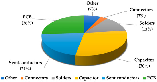
Figure 1.
Distribution of failures in power devices [9].
There are two types of faults in semiconductor switching devices: open-circuit and short-circuit. An open-circuit fault can be caused by a gate driver malfunction, a momentary short circuit, or damage to any inner wire. The reason behind the short-circuit fault may be due to over-voltage, over-current and wrong gate signal [11]. In the case of short-circuit faults of the semiconductor switches, the removal becomes difficult, as it incorporates additional hardware circuits for fault detection and tolerance [12].
Several authors have suggested various methods to tolerate faults, thereby increasing the reliability of the converter system of the conventional MLI topologies such as Neutral Point Clamped (NPC) [13,14], Flying Capacitor (FC) [15,16] and Cascaded H-Bridge [17,18].
In [19], to improve the reliability of the CHB multilevel inverter, one additional leg (consisting of two semiconductor switches) and four triacs are utilized, although it is not economically feasible. In [20], a modified topology of [19] is presented, without using any additional leg and with four triacs. In [21], a switch is put between the DC sources and the load, although the fault in two switches is not taken into account. The authors in [22] discuss a Fault-Tolerant Hybrid Cascaded H-Bridge Multilevel Inverter, although the failure in DC-link capacitors causes discontinuity of operation.
Recently, some topologies for reduced device-MLIs with the ability to tolerate faults have been introduced [23]. The availability of redundant states, i.e., numerous switching states that can provide the same inverter output voltage levels, is the most significant need for fault-tolerant MLIs [24]. Whenever a fault occurs, the lack of redundant states can cause the malfunction or complete shutdown of the MLIs [25]. The problem with the reduced-device MLIs is that there is lack of redundant states and hence the probability of being fully fault-tolerant is very difficult. The reliability of the reduced-device MLIs can be increased by raising the number of redundant states and this is done by adding one or more power semiconductor devices in parallel to the existing devices [26].
In [12], the authors propose an open-circuit fault detection and elimination technique of a 3-level T-Type MLI where the fault is detected by sensing the capacitor voltage. This topology is not fully fault-tolerant, although the topology in [27] is fully fault-tolerant without any loss of levels in the output voltage, but has the drawback of more switching device and capacitor requirement. However, the FT topology in [27] does not need any external circuitry for the balancing of the capacitor voltage for the fault in the switch closer to the DC link; this cannot be tolerated, as it unbalances the capacitor voltage.
The fault diagnostic method can be categorized into two types: material redundancy and analytical redundancy [28,29]. The material redundancy technique entails having extra elements to replace the faulty components, allowing the system to isolate the fault and operate in faulty conditions. This procedure involves connecting an auxiliary branch or device across the converter or part of the converter, substituting the broken branch and allowing power to flow continuously [30]. The analytical redundancy method consists in the addition of a block in the control system capable of reconfiguring the output signals using the feedback from these signals [31].
In this paper, we have followed the material redundancy fault diagnostic method, where parallel switches are connected across the switches that cause shutdown of the system. A multilevel inverter design with nine levels in output voltage during normal conditions is discussed for use with single-switch open-circuit failures in the semiconductor switching devices. The concepts and the design are verified by simulating using MATLAB/Simulink followed by experimental verification.
The remainder of this paper is structured as follows: Section 2 discusses the existing MLI topology, and fault diagnosis is performed for every switch. The proposed fault-tolerant topology, as well as its operating principle are described in Section 3. The modulation strategy is discussed in Section 4, and the simulation results are shown in MATLAB/Simulink, followed by experimental validation and power loss analyses using PLECS in Section 5. Section 5 also compares the proposed fault-tolerant topology with other fault-tolerant topologies that have recently been presented. The work is brought to a conclusion in Section 6.
2. Existing Nine-Level MLI Topology
The existing nine-level Packed-E-Cell [32,33] inverter has six active bidirectional switches and two DC capacitors which are shunted by a four -quadrant switch to form an E-cell. The DC capacitors are balanced using the redundant charging/discharging states by properly designing the corresponding PEC9 switching states. Due to the horizontal placement of the shunted capacitors, both the capacitors are charged and discharged simultaneously with the redundant states; hence, only the auxiliary DC-link voltage has to be measured and maintained at half of the DC source voltage, and this inherently balances the voltage across the DC capacitors to one-fourth of the DC source voltage. Along with a reduced component count, the E-cell also helps the proposed topology to attain multi ac terminal operation, i.e., if there is a fault in the four-quadrant switch, the PEC9 MLI topology continues to operate as five-level, thereby increasing the reliability.
The existing nine-level PEC MLI is composed of six active unidirectional switches S1, S2, S3, S4, S5 and S6; one four-quadrant switch S7, a single DC source Vdc and two capacitors C1 and C2, as shown in Figure 2. The four-quadrant switch is connected between the midpoint of the two capacitors C1 and C2 and the inverter ac terminal point. A single auxiliary DC-link is created by placing the two capacitors in horizontal position, so that both the capacitors are accordingly charged and discharged. This provides a synchronism between both the capacitors during charging and discharging. Due to the presence of the four-quadrant switch, the E-cell provides multiple voltage levels, i.e., five, seven or nine at the output, without changing the structure.
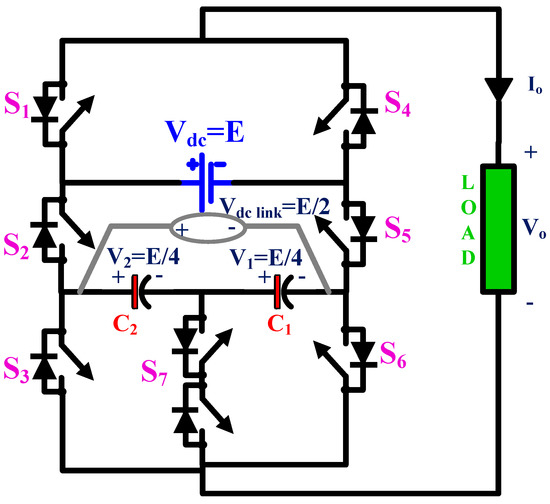
Figure 2.
Existing configuration of nine-level MLI [32].
There are 24 switching states for the existing nine level PEC9 MLI for both directions of current denoted by µi (I = 1, 2,…, 24), as shown in Table 1. During the operation, all the switches, capacitors and diodes are assumed to be ideal, and the effect of parasitic components is not included. The conducting paths for load current Io greater than zero are shown as dark lines for each mode of operation, in Figure 3.

Table 1.
Switching States of the nine-level PEC9 MLI.
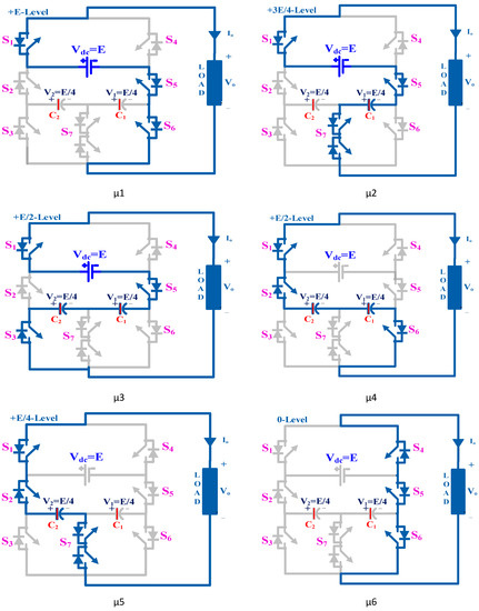
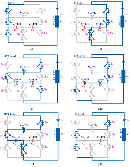
Figure 3.
Conduction paths of existing 9-level PEC9 topology.
The existing PEC9 MLI is investigated for open-circuit faults as shown in Table 2. If one of the switches of either S2 or S5 undergoes failure (open-circuit fault), existing PEC9 topology can produce three-level output voltage. If either of the switches S3 or S6 fails to operate, then the operation can continue with seven-level output voltage. For failure in the four-quadrant switch S7, the existing topology can operate with five levels in the output voltage.
Table 2.
Operating modes for single-switch open-circuit fault in existing PEC9 MLI.
On the other hand, if switch S1 or S4 undergoes an OC fault, then no operating MLI modes will allow the synthesis of output voltage across the load, and the corresponding condition will be equivalent to a shutdown.
3. Modified Nine-Level PEC9 FT MLI
The modified topology (PEC9 FT) is achieved by adding two more switches S8 and S9 to the existing single-phase PEC9 topology. The added switches in parallel to S1 and S4 provide additional redundant states so that an alternative path is available when either of the switches S1 and S4 undergoes open-circuit fault, and the topology will not undergo complete shutdown. The modified topology is shown in Figure 4.
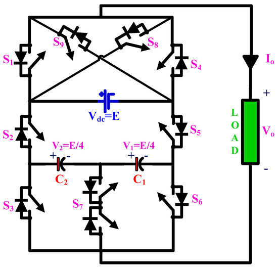
Figure 4.
The Modified PEC9 FT MLI Topology.
With this modification, there is an increase in the number of redundant switching states. There is one output voltage level produced by each switching state in the Modified PEC9 FT MLI topology, and when all such levels are combined a nine-level periodic voltage is achieved at the output. Table 3 shows all the switching states of PEC9FT-MLI, along with the outputs. Table 3 shows that if there is an open-switch fault in any of the switches S2, S3, S5, S6 and S7, there is still conversion of power from source to load; however, with reduced output voltage levels of seven, five or three, according to the switch location. However, if the open-switch fault occurs in switches S1 or S4 or any other switch pair, the post-fault output has the same magnitude and levels as it had in the pre-fault condition. This certainly improves the reliability when critical loads are supplied.
Table 3.
Operating modes of FT-MLI topology for PEC9 FT MLI.
4. Modulation Strategy
In this paper, optimized nearest level control (ONLC) is used for generating the control signals. ONLC is one of the subsets of the nearest level control scheme (NLC) [34], which is a fundamental frequency switching scheme. NLC is generally of three types: conventional NLC, modified NLC and optimized NLC. Amongst the three, ONLC is preferred as the value of THD is less in ONLC compared with conventional and modified NLCs for both a low number of levels and a high number of levels. In the optimized NLC method, the comparison value is taken as 0.4 instead of the half-integer value 0.5 (i.e., 1.5 is rounded off as 2 and 1.3 is rounded off as 1). The DC loss error between two levels is always maintained as 0.4 Vdc. The comparison of the sinusoidal reference signal Vref and the carrier signals is shown in Figure 5, and the block diagram of the nearest level prediction is shown in Figure 6. The carrier constant is set to 0.4 in the optimized NLC technique, which minimizes THD while also increasing the RMS value of output voltage and current. The three important parameters considered to select the optimum constant value are as follows: the presence of odd harmonics content in output voltage, various constant carrier values, and output RMS voltage value. The RMS value is higher in the nearest value at 0.1 and decreases gradually at point 1.0, which gives a low RMS voltage value. But in the case of THD, it is variable, with different nearest values. For ‘N’ level output voltage, the total number of carrier signals (B1 to Bn) required are as follows:
where n = (N − 1)/2
| B1 | B2 | B3 | B4 | …… | Bn−1 | Bn |
| 0.4 | 1 + 0.4 | 2 + 0.4 | 3 + 0.4 | …… | (n − 2) + 0.4 | (n − 1) + 0.4 |
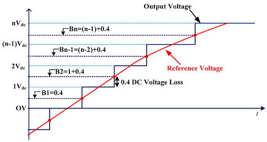
Figure 5.
Level generation method of optimized nearest level control.
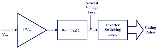
Figure 6.
Block diagram of optimized NLC.
The switching angle for the optimized NLC can be found using the equation below:
where p = 1, 2, 3, …, (N − 1)/2.
5. Results and Discussion
5.1. Simulation Results
The open loop simulation of the modified proposed FT MLI is performed using the optimized nearest level control (ONLC) technique with MATLAB/Simulink software. Simulation was carried out to obtain the waveforms of single-phase output voltage, current through the load, and THD in the output voltage for R-L Load. The component parameters used in the simulation of existing PEC9 MLI are listed in Table 4.
Table 4.
Simulation parameters for the proposed FT MLI.
Figure 7a–g shows the waveform for the voltage at the output, current through the load and the voltage across capacitors under pre-fault condition (t < 0.04 s), during-fault condition (0.04 < t < 0.08 s) and post-fault condition (t > 0.08 s). When an open-circuit fault occurs in switches S1, S4, S8, and S9 at t = 0.04 s, the post-fault output voltage levels remain the same as that of a healthy condition at nine with a peak value of 100 V, and the load current post fault remains at the same peak magnitude as in normal conditions. The proposed design reduces the post-fault output voltage levels from nine to seven for an open-circuit fault in the switches S3 and S6, as well as reducing the peak magnitude of the load current. When the four-quadrant switch S7 experiences an open-circuit fault, the output voltage levels drop from nine to five, along with the reduction in amplitude of the load current. In the case of an open-circuit fault in switches S2 and S5, the post-fault voltage has three levels, with a peak value of 50 V along with a balanced current with reduced peak value. The simulation results show that the proposed fault-tolerant topology has the benefit of allowing power conversion to continue even if one of the switches has an open-circuit failure.
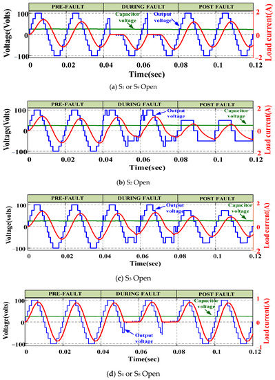
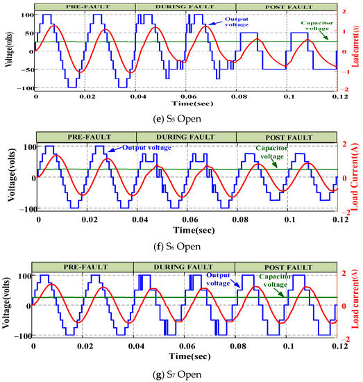
Figure 7.
Waveforms obtained from the simulation for the voltage at the output, current through the load and voltage across the capacitor for pre-fault, faulty and post-fault conditions in: (a) S1 or S8, (b) S2, (c) S3, (d) S4 or S9 (e) S5 (f) S6 and (g) S7.
The voltage across the capacitors C1 and C2 as shown in Figure 7 remains constant, with a value of Vdc/4, i.e., 25 volts for the given supply of 100 Volts.
Figure 8 presents the simulation results of the voltage THD after the fault has been cleared. Figure 8a shows the output voltage THD profile after the faults in switches S1, S4, S8 or S9 have been cleared. Similarly, Figure 8b–d shows the THD profile for the output voltage for faults in switches S3 or S6, S7, and S2 or S5, respectively.
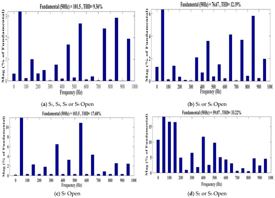
Figure 8.
Simulation results of Voltage THD profiles after clearing of faults in (a) S1, S4, S8 or S9 (b) S3 or S6 (c) S7, and (d) S2 or S5.
5.2. Experimental Results
The above-mentioned simulation results for the suggested fault-tolerant multilevel inverter design were verified using an experimental prototype, as shown in Figure 9. Table 5 shows the parameters used for obtaining the experimental results.
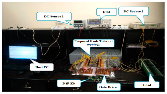
Figure 9.
Experimental setup for the proposed fault-tolerant topology.
Table 5.
Parameters of experimental validation.
The pre-fault, during-fault, and post-fault waveforms for output voltage, load current, and capacitor voltages are shown in Figure 10. For open-circuit faults in switches S1, S4, S8 or S9 the post-fault output voltage contains nine levels, and the peak is maintained at 120 V, as shown in Figure 10a,d. For open-circuit faults in S2 or S5, the output voltage levels reduce to three, and peak output voltage reduces to 60 Volts, as shown in Figure 10b,e. For open-circuit faults in switches S3 and S6, the post-fault output voltage reduces to seven levels and a peak value of 90 V, as shown in Figure 10c,f. For an open-switch fault in S7 the post-fault output voltages are reduced to five, with a peak value of 120 V, as shown in Figure 10g. Figure 10h shows the voltage across each capacitor maintained at 30 V for the pre-fault, during-fault and post-fault conditions for any of the switches.
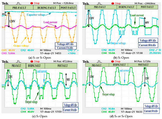
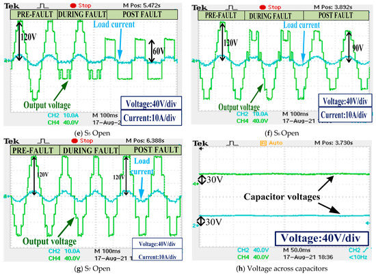
Figure 10.
Experimental results: voltage across the output and current through the load waveform showing pre-fault, during-fault and post-fault conditions for switches; (a) S1 or S8 (b) S2, (c) S3, (d) S4 or S8, (e) S5 and (f) S6; (g) S7 Open, (h) voltage across capacitors for fault across each switch.
Figure 11 represents the experimental validation of the output voltage THD after the fault has been cleared. Figure 11a shows the output voltage THD profile after the faults in switches S1, S4, S8 or S9 have been cleared. Similarly Figure 11b–d shows the THD profile for the output voltage for faults in switches S3 or S6, S7, and S2 or S5, respectively.
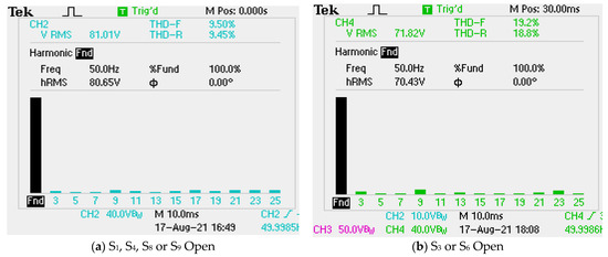
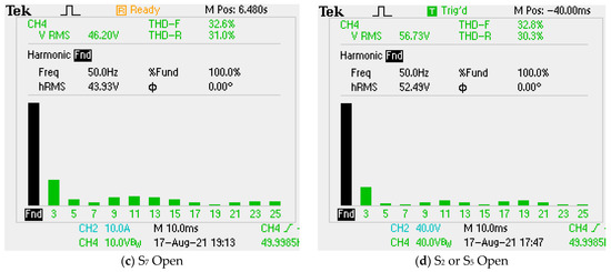
Figure 11.
Experimental verification of Voltage THD profiles for clearing of faults in: (a) S1, S4, S8 or S9, (b) S3 or S6, (c) S7 and (d) S2 or S5.
5.3. Power Loss Analysis
PLECS (Piecewise Linear Electrical Circuit Simulation) software was used to assess power and efficiency losses in the overall sense of the recommended topology. Thermal modeling in the software was used to calculate precise conduction and switching losses for all switches, as well as losses across the capacitors. Infineon’s IGBT switch IGA30N60H3 was used for this work. Figure 12 depicts the IGBT’s turn ON, turn OFF, and conduction loss models. Switching losses (PS) and conduction losses (PC) of all semiconductor devices, as well as ripple loss (PR) of capacitors, were considered in this study.
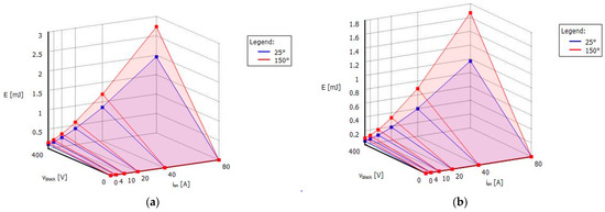
Figure 12.
Loss model for (a) turn ON, (b) turn OFF, and (c) conduction loss for IGBT IGA30N60H3.
5.3.1. Switching Losses
Switching losses occurred at the instant the switches were turned on or off. Taking into account the approximation in a linear sense between the current and the voltage of switches throughout the switching period, the following equations may be written for the kth switch:
Loss of power during switching ON:
Loss of power during switching OFF:
where and denote currents across the kth switch when it has been turned ON, and prior to turning it OFF, respectively, f is the frequency of switching, and denotes the voltage for the OFF-state of the kth switch. For calculating the loss in switching in total, the ON () and the OFF number of switching states () for each cycle are multiplied with (1) and (2) following (3):
5.3.2. Conduction Losses (PC)
To quantify losses in conduction in the steady-state condition, the internal resistance of each component, such as the semiconductor devices and capacitors, had to be addressed. The capacitors were expected to be identical. Because the condition of resistive loading is believed to be the worst-case scenario in the study of loss of power for the SCMLIs, the results were collected using the PLECS software for a resistive load.
5.3.3. Capacitor Ripple Losses (PR)
Ripple losses occur because of the difference between the input voltage (Vin) and the voltage across the capacitors (Vcj (j = 1, 2, 3, 4)), when the capacitors are connected in parallel. It is assumed that the capacitor is fully charged to Vin during the charging state.
The capacitor ripple voltage is taken as:
Here, denotes passing current of the jth capacitor. The discharging period is . Thus, the total ripple loss in the duration of the output waveform cycle is given by (7).
It is clear from (6) and (7) that ripple loss is in inverse proportion to capacitance. As a result, more capacitance resulted in reduced ripple loss and, as a result, increased efficiency. The efficiency of the overall proposed inverter is given by (8).
Figure 13 shows the efficiency vs load power factor curve for the proposed fault-tolerant MLI for various modulation indices. For both setups in which capacitor ripple loss was ignored, maximum efficiency was around 98.7%, and a 100-watt output power was attained. In its place, capacitor ESR loss (conduction loss owing to internal resistance of the capacitors (here 0.1 ohm)) was used.
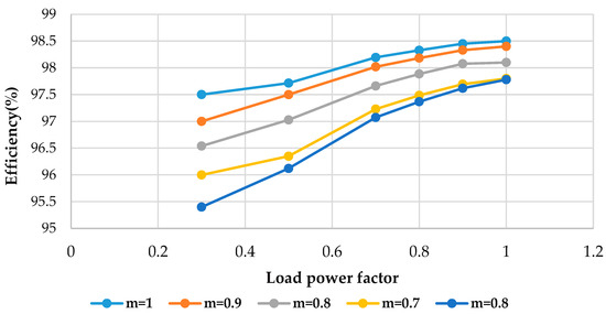
Figure 13.
Efficiency versus load power factor curve of the proposed fault-tolerant MLI.
5.4. Comparison with Recent Topologies
This section compares the proposed fault-tolerant multilevel inverter with recently developed fault-tolerant topologies that produce nine levels as output during the pre-fault/normal conditions. The suggested fault-tolerant topology is compared, based on the number of DC sources, capacitors, switches, and bidirectional switches. The comparison is made in tabular form as shown in Table 6. In terms of the number of IGBT switches and DC sources, the suggested fault-tolerant topology is more cost-effective than other compared topologies.
Table 6.
Comparison of various parameters of the proposed FT MLI topology with other recently developed topologies.
6. Conclusions
This paper presents a multilevel inverter topology that is fault-tolerant; its comparison with other recently proposed fault-tolerant multilevel inverters proves its capability. The proposed topology includes redundant circuit paths that help give output even if the power switches are open-circuited, making it entirely fault-tolerant. The capacitors’ self-voltage balancing is maintained inherently under pre-fault, fault, and post-fault conditions. The optimized nearest level control technique is used for simulation and the results obtained from the experiments validate its adaptability against open-circuit faults. Simulation and experimental verification are used to verify the practicality of the proposed topology.
Author Contributions
Conceptualization, A.S.; Formal analysis, S.A.K., A.S., M.T., S.U. and M.A.H.; Funding acquisition, S.U.; Investigation, S.A.K., A.S., M.T., S.U. and M.A.H.; Methodology, S.A.K., A.S., M.T. and M.A.H.; Project administration, S.U.; Supervision, A.S. and M.T.; Writing—original draft, S.A.K., A.S. and M.T.; Writing—review & editing, S.U. and M.A.H. All authors have read and agreed to the published version of the manuscript.
Funding
This research is funded by Princess Nourah bint Abdulrahman University Researchers Supporting Project number (PNURSP2022R79), Princess Nourah bint Abdulrahman University, Riyadh, Saudi Arabia.
Acknowledgments
Princess Nourah bint Abdulrahman University Researchers Supporting Project number (PNURSP2022R79), Princess Nourah bint Abdulrahman University, Riyadh, Saudi Arabia.
Conflicts of Interest
The authors declare no conflict of interest.
References
- Franquelo, L.G.; Rodriguez, J.; Leon, J.I.; Kouro, S.; Portillo, R.; Prats, M.A. The age of multilevel converters arrives. IEEE Ind. Electron. Mag. 2008, 2, 28–39. [Google Scholar] [CrossRef]
- Abu-Rub, H.; Holtz, J.; Rodriguez, J.; Baoming, G. Medium-voltage multilevel converters—State of the art, challenges, and requirements in industrial applications. IEEE Trans. Ind. Electron. 2010, 57, 2581–2596. [Google Scholar] [CrossRef]
- Chappa, A.; Gupta, S.; Sahu, L.K.; Gautam, S.P.; Gupta, K.K. Symmetrical and Asymmetrical Reduced Device Multilevel Inverter Topology. IEEE J. Emerg. Sel. Top. Power Electron. 2019, 9, 885–896. [Google Scholar] [CrossRef]
- Liu, Y.; Ge, B.; Abu-Rub, H.; Peng, F.Z. An Effective Control Method for Quasi-Z-Source Cascade Multilevel Inverter-Based Grid-Tie Single-Phase Photovoltaic Power System. IEEE Trans. Ind. Inform. 2013, 10, 399–407. [Google Scholar] [CrossRef]
- Debnath, S.; Saeedifard, M. A New Hybrid Modular Multilevel Converter for Grid Connection of Large Wind Turbines. IEEE Trans. Sustain. Energy 2013, 4, 1051–1064. [Google Scholar] [CrossRef]
- Haw, L.K.; Dahidah, M.S.A.; Almurib, H. SHE–PWM Cascaded Multilevel Inverter With Adjustable DC Voltage Levels Control for STATCOM Applications. IEEE Trans. Power Electron. 2014, 29, 6433–6444. [Google Scholar] [CrossRef]
- Jung, J.-J.; Cui, S.; Lee, J.-H.; Sul, S.-K. A new topology of multilevel VSC converter for a hybrid HVDC transmission system. IEEE Trans. Power Electron. 2016, 32, 4199–4209. [Google Scholar] [CrossRef]
- Feldman, R.; Tomasini, M.; Amankwah, E.; Clare, J.C.; Wheeler, P.W.; Trainer, D.R.; Whitehouse, R.S. A Hybrid Modular Multilevel Voltage Source Converter for HVDC Power Transmission. IEEE Trans. Ind. Appl. 2013, 49, 1577–1588. [Google Scholar] [CrossRef]
- Yang, S.; Xiang, D.; Bryant, A.; Mawby, P.; Ran, L.; Tavner, P. Condition Monitoring for Device Reliability in Power Electronic Converters: A Review. IEEE Trans. Power Electron. 2010, 25, 2734–2752. [Google Scholar] [CrossRef]
- Choupan, R.; Golshannavaz, S.; Nazarpour, D.; Barmala, M. A new structure for multilevel inverters with fault-tolerant capability against open circuit faults. Electr. Power Syst. Res. 2018, 168, 105–116. [Google Scholar] [CrossRef]
- Mirafzal, B. Survey of Fault-Tolerance Techniques for Three-Phase Voltage Source Inverters. IEEE Trans. Ind. Electron. 2014, 61, 5192–5202. [Google Scholar] [CrossRef]
- Choi, U.-M.; Lee, K.-B.; Blaabjerg, F. Diagnosis and Tolerant Strategy of an Open-Switch Fault for T-Type Three-Level Inverter Systems. IEEE Trans. Ind. Appl. 2013, 50, 495–508. [Google Scholar] [CrossRef]
- Caseiro, L.; Cruz, S.; Mendes, A. Fault tolerance in back-to-back three-level neutral-point-clamped induction motor drives. In Proceedings of the 7th IET International Conference on Power Electronics, Machines and Drives (PEMD 2014), Manchester, UK, 8–10 April 2014. [Google Scholar] [CrossRef]
- Ceballos, S.; Pou, J.; Robles, E.; Gabiola, I.; Zaragoza, J.; Villate, J.L.; Boroyevich, D. Three-Level Converter Topologies With Switch Breakdown Fault-Tolerance Capability. IEEE Trans. Ind. Electron. 2008, 55, 982–995. [Google Scholar] [CrossRef]
- Richardeau, F.; Pham, T.T.L. Reliability Calculation of Multilevel Converters: Theory and Applications. IEEE Trans. Ind. Electron. 2012, 60, 4225–4233. [Google Scholar] [CrossRef]
- Druant, J.; Vyncke, T.; De Belie, F.; Sergeant, P.; Melkebeek, J. Adding inverter fault detection to model-based predictive control for flying-capacitor inverters. IEEE Trans. Ind. Electron. 2014, 62, 2054–2063. [Google Scholar] [CrossRef]
- Kandasamy, K.; Vilathgamuwa, M.; Tseng, K.J. Inter-module state-of-charge balancing and fault-tolerant operation of cascaded H-bridge converter using multi-dimensional modulation for electric vehicle application. IET Power Electron. 2015, 8, 1912–1919. [Google Scholar] [CrossRef]
- Song, W.; Huang, A.Q. Fault-Tolerant Design and Control Strategy for Cascaded H-Bridge Multilevel Converter-Based STATCOM. IEEE Trans. Ind. Electron. 2009, 57, 2700–2708. [Google Scholar] [CrossRef]
- Song, Y.; Wang, B. Analysis and Experimental Verification of a Fault-Tolerant HEV Powertrain. IEEE Trans. Power Electron. 2013, 28, 5854–5864. [Google Scholar] [CrossRef]
- Kumar, V.V.S.P.; Fernandes, B.G. A Fault-Tolerant Single-Phase Grid-Connected Inverter Topology with Enhanced Reliability for Solar PV Applications. IEEE J. Emerg. Sel. Top. Power Electron. 2017, 5, 1254–1262. [Google Scholar] [CrossRef]
- Sivakumar, K. A Fault-Tolerant Single-Phase Five-Level Inverter for Grid-Independent PV Systems. IEEE Trans. Ind. Electron. 2015, 62, 7569–7577. [Google Scholar] [CrossRef]
- Mhiesan, H.; Wei, Y.; Siwakoti, Y.P.; Mantooth, H.A. A Fault-Tolerant Hybrid Cascaded H-Bridge Multilevel Inverter. IEEE Trans. Power Electron. 2020, 35, 12702–12715. [Google Scholar] [CrossRef]
- Prakash, G.; Subramani, C.; Bharatiraja, C.; Shabin, M. A low cost single phase grid connected reduced switch PV inverter based on Time Frame Switching Scheme. Int. J. Electr. Power Energy Syst. 2016, 77, 100–111. [Google Scholar] [CrossRef]
- Dewangan, N.K.; Gupta, S.; Gupta, K.K. Approach to synthesis of fault tolerant reduced device count multilevel inverters (FT RDC MLIs). IET Power Electron. 2019, 12, 476–482. [Google Scholar] [CrossRef]
- Vijeh, M.; Rezanejad, M.; Samadaei, E.; Bertilsson, K. A General Review of Multilevel Inverters Based on Main Submodules: Structural Point of View. IEEE Trans. Power Electron. 2019, 34, 9479–9502. [Google Scholar] [CrossRef]
- Kumar, D.; Nema, R.K.; Gupta, S. Investigation of fault-tolerant capabilities of some recent multilevel inverter topologies. Int. J. Electron. 2021, 108, 1957–1976. [Google Scholar] [CrossRef]
- Chen, A.; Hu, L.; Chen, L.; Deng, Y.; He, X. A Multilevel Converter Topology with Fault-Tolerant Ability. IEEE Trans. Power Electron. 2005, 20, 405–415. [Google Scholar] [CrossRef]
- Aguayo-Alquicira, J.; Vásquez-Libreros, I.; De Léon-Aldaco, S.; Ponce-Silva, M.; Lozoya-Ponce, R.; Flores-Rodríguez, E.; García-Morales, J.; Reyes-Severiano, Y.; Carrillo-Santos, L.; Marín-Reyes, M.; et al. Reconfiguration Strategy for Fault Tolerance in a Cascaded Multilevel Inverter Using a Z-Source Converter. Electronics 2021, 10, 574. [Google Scholar] [CrossRef]
- Jalhotra, M.; Kumar, L.; Gautam, S.P.; Gupta, S. Development of fault-tolerant MLI topology. IET Power Electron. 2018, 11, 1416–1424. [Google Scholar] [CrossRef]
- Kwak, Y.-G.; Heo, D.-H.; Kim, S.-P.; Song, S.-G.; Park, S.-J.; Kang, F.-S. Reliability and Economic Efficiency Analysis of 4-Leg Inverter Compared with 3-Leg Inverters. Electronics 2021, 10, 87. [Google Scholar] [CrossRef]
- Abbasi, S.; Ghadimi, A.A.; Abolmasoumi, A.H.; Miveh, M.R.; Jurado, F. Enhanced Control Scheme for a Three-Phase Grid-Connected PV Inverter under Unbalanced Fault Conditions. Electronics 2020, 9, 1247. [Google Scholar] [CrossRef]
- Sharifzadeh, M.; Al-Haddad, K. Packed E-Cell (PEC) Converter Topology Operation and Experimental Validation. IEEE Access 2019, 7, 93049–93061. [Google Scholar] [CrossRef]
- Sharifzadeh, M.; Babaie, M.; Sebaaly, F.; Mehrasa, M.; Chouinard, G.; Al-Haddad, K. Low Switching Frequency Operation of PEC9 Multilevel Inverter Using Modified SHM-PWM. In Proceedings of the IECON 2020 the 46th Annual Conference of the IEEE Industrial Electronics Society, Singapore, 18–21 October 2020; pp. 4215–4220. [Google Scholar] [CrossRef]
- Hu, P.; Jiang, D. A Level-Increased Nearest Level Modulation Method for Modular Multilevel Converters. IEEE Trans. Power Electron. 2014, 30, 1836–1842. [Google Scholar] [CrossRef]
- Dewangan, N.; Jalhotra, M.; Sahu, L.K.; Gautam, S.P.; Gupta, S. Fault Tolerant Analysis of Single Phase Multilevel Inverter. In Proceedings of the 2018 IEEE International Conference on Power Electronics, Drives and Energy Systems (PEDES), Chennai, India, 18–21 December 2018; pp. 1–6. [Google Scholar] [CrossRef]
- Kumar, V.; Singh, S.; Jain, S. Fault Tolerant T-Type Cross Connected Source Nine Level Inverter. In Proceedings of the 2020 IEEE 9th Power India International Conference (PIICON), Murthal, India, 28 February–1 March 2020; pp. 1–6. [Google Scholar] [CrossRef]
- Chappa, A.; Gupta, S.; Sahu, L.K.; Gupta, K.K. A Fault-Tolerant Multilevel Inverter Topology With Preserved Output Power and Voltage Levels Under Pre- and Postfault Operation. IEEE Trans. Ind. Electron. 2020, 68, 5756–5764. [Google Scholar] [CrossRef]
- Kumar, M.S.; Borghate, V.B.; Karasani, R.R.; Sabyasachi, S.; Suryawanshi, H.M. A fault-tolerant modular multilevel inverter topology. Int. J. Circuit Theory Appl. 2018, 46, 1028–1043. [Google Scholar] [CrossRef]


Publisher’s Note: MDPI stays neutral with regard to jurisdictional claims in published maps and institutional affiliations. |
© 2022 by the authors. Licensee MDPI, Basel, Switzerland. This article is an open access article distributed under the terms and conditions of the Creative Commons Attribution (CC BY) license (https://creativecommons.org/licenses/by/4.0/).