Abstract
This paper presents the theoretical analysis, experimental results and generalized structure for N modules of an isolated dc–dc SEPIC converter. The structure comes from the integration of N conventional SEPIC converters based on the input-series and output-parallel connection. The main advantages provided by the proposed structure are reduced voltage stress across the semiconductors and division of the current stress in the output diodes. The proposed converter is presented in a generalized approach, varying the voltage stress across the semiconductors according to the number of modules used. As the converter uses more than one switch, the commands can be either equal or phase-shifted by degrees. When operating with phase-shift modulation, a multilevel converter is obtained, which brings another advantage of the structure, since there is a reduction in the volume of the input inductors ( and ) and the output capacitor (). In this paper, the steady-state analysis, a dynamic model, system control and experimental results are presented for phase-shift modulation and discontinuous conduction mode (DCM). The performance of the proposed converter was verified in a prototype with four modules and the following specifications: 500 W output power, 800 V input voltage, 120 V output voltage and 50 kHz switching frequency. The converter achieved 94.42% efficiency at rated power.
1. Introduction
In recent years, the implementation of dc grids integrated with renewable sources and dc loads has been presented as a new configuration for the grids of the future [1,2,3]. The power processing in microgrids is managed by converters and, in the case of dc grids, by dc–dc converters, which has significantly increased the demand for new converters [1,2,3]. The bus voltage of the dc networks is an important parameter, as it determines factors such as losses, isolation, system safety, and, most notably, the voltage levels at which the converters will operate [4]. When a bus voltage of 800 V or more is used, the voltage stresses that the semiconductors will be submitted to must be analyzed carefully because, in some structures, these stresses can be relatively high [5,6,7]. Studies that relate the viability of a dc system and voltage levels have been reported in [8,9]. Among the various voltage and power levels of a microgrid, there are commercial and residential applications, which include low power loads [9,10,11].
In many applications, galvanic isolation between the input and output is desirable to isolate the power supply from the load [12]. The challenge of isolated structures is the overvoltage on the semiconductors due to the presence of the leakage inductance, which increases when the transformer turns ratio is different from unity. In order not to oversize the semiconductors, which could generate a decrease in the efficiency of the structure, it is necessary to use a snubber circuit to avoid failures in these semiconductors [13,14,15]. Thus, for applications involving input voltage values from 600 to 2000 V, dc–dc converters able to provide reduced stress across the semiconductors are sought.
The literature has presented a significant number of studies for dc–dc step-down converters, mainly isolated buck converters, for a wide range of power and voltage levels [16,17,18]. The isolated topologies group, such as full-bridge, half-bridge, flyback and forward, can provide output voltages either lower or higher than the input voltage just using the transformers turns ratio. However, once designed as a step-up, the converter will always operate as such, or if it was designed as a step-down, it will just operate as a step-down. Thus, the conventional isolated converters are not suitable for design specifications with a wide input voltage range.
The dc–dc converters operating with high voltage levels (in input and/or output) present challenges in relation to voltage stress on the semiconductors. This challenge is higher for step-down/step-up converters (as SEPIC, Cuk, Zeta, flyback) due to the theoretical maximum voltage across the semiconductor being equal to the sum of input and output voltages. The series connection of components or modules is a method to overcome this challenge, for instance, as in the input-series-output-parallel (ISOP) [19,20,21,22], the input-series-output-series (ISOS) [23,24], and the input-parallel-output-series (IPOS) converters [25,26,27]. However, the literature is lacking solutions using module connection to increase the voltage range of dc–dc step-down/step-up converters, such as SEPIC, which is the focus of this research.
Two other methods that should also be noted are the stacking of a number of converters [28] and low-power multilevel topologies [29]. In the stacking converters, the stacked cells increase or decrease the voltage gain compared to the single converter cell [30]. In [28], a stacked flyback converter operating as a voltage step-down converter is presented. An interesting solution for low-power applications is proposed in [29], which is based on the isolated three-level SEPIC converter. However, the cited paper presents only a brief analysis of the structure and numerical simulation results; i.e., the subject needs to be further explored.
SEPIC converter-derived topologies feature dc current at the input with low ripple [31,32] and output with a voltage source characteristic, and they operate as a step-up/step-down voltage regulator without reversing the polarity of the output voltage. SEPIC structures are widely used in several applications including renewable energy [33,34], battery chargers [35] and LED lighting drivers [36,37], and also to perform power factor correction [38,39,40,41].
In the light of the current challenges, this paper presents a multilevel structure based on the isolated SEPIC converter. The structure results from the integration of N SEPIC converters with the output connected in parallel, reducing the voltage stress on the semiconductors. In addition, the reduction of the stresses on the semiconductors allows selecting lower drain-source breakdown voltage components, which are cheaper, present better performance in terms of efficiency, and provide fewer switching problems due to the lower dv/dt. With the characteristics presented, the converter can be used in LED lighting drivers and in dc microgrids with voltages above 400 V. In [42], the structure with two modules was briefly presented. However, the main features and contributions of the structure were not addressed. In this paper, the generalization of the structure, mathematics analysis, and experimental results are presented in detail.
The following sections report the principles of operation, modulation, generalization, design equations, control strategy, dynamic model, prototype, experimental results, comparisons, and conclusions.
2. Generalization of Proposed Converter
The proposed topology is based on the conventional dc–dc SEPIC converter, and it is generated from the inclusion of modules (N), as can be seen in Figure 1. Each module consists of a switch (S), a coupled inductor () and a diode (D). The input capacitors () alternate in different configurations, using N capacitors when N is even and N + 1 capacitors when N is odd. These capacitors have the function of exchanging energy with the circuit and not shorting the switches; that is, they are input SEPIC capacitors. The input inductors ( and ) and the output capacitor () remain constant, regardless of the number of modules.
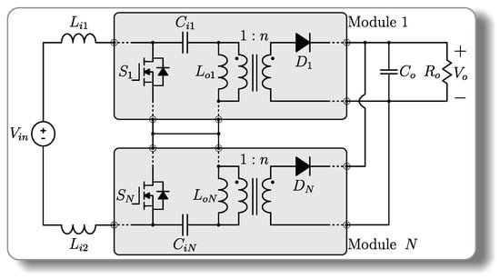
Figure 1.
Generalization of the proposed structure.
The proposed integration reduces the voltage stress on the semiconductors, since the input voltage () is divided by the number of modules, as can be seen in
and
It should be noted that for the same input and output () voltage level and a fixed turns ratio , the maximum voltage across the switches and diodes decreases with the addition of modules. On the other hand, for the same voltage stress across the switches and diodes, the input or output levels can be increased (mainly the input voltage).
The proposed converter characteristics solve the critical challenge of high-voltage stress on the switch present in conventional SEPIC converters. Thus, components with a lower drain-source breakdown voltage can be selected, reducing the cost of the structure, with better performance in terms of efficiency and less switching problems due to the lower level of operating voltage. In addition, the output of the N-based converters is parallel-connected, allowing division of the current stress in the output diodes.
On the other hand, when the number of modules increases, the number of components will also increase, which is the main drawback of the proposed solution (a typical disadvantage of modular connection). Figure 2a–c show the proposed topology with two (N = 2), three (N = 3) and four (N = 4) modules, respectively.
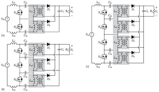
Figure 2.
Proposed structure of the dc–dc converter with: (a) two modules, (b) three modules and (c) four modules.
Table 1 gives the number of components as a function of the number of modules. Analyzing Table 1, it can be seen that regardless of the number of modules used, the number of input inductors and output capacitor remain constant (being equal to one). The switches, diodes and coupled inductors increase as the number of modules increases, as
where , and are the number of switches, diodes and coupled inductors, respectively.

Table 1.
Number of components as a function of the number of modules.
The amount of input capacitors () increase in a particular way. For N = 1, the converter has one input capacitor ( = 1). When the converter operates with two modules (N = 2), it has two input capacitors ( = 2). In these two situations, the number of input capacitors can be represented by
When the number of modules is greater than or equal to three, two cases must be analyzed: if N is even, the number of input capacitors is given by (4); if N is odd, the number of input capacitors is determined by
Figure 3 presents an analysis of the parameterized stress across the switches, diodes and capacitors and , as a function of the number of modules. The voltage stress values are given in pu (per-unit), normalized by the input voltage, considering constant output voltage and turns ratio. As the number of modules increases, the stress across the semiconductors will decrease. However, from N = 4, the rate of reduction decreases. Therefore, the use of the converter with five or more modules is not attractive, since the number of components increases significantly. The voltage stress on capacitor is equal to the input voltage for the conventional SEPIC converter (N = 1) and equal to half the input voltage for the converter operating from two modules. The lowest voltage stress on the capacitor occurs when N = 3.
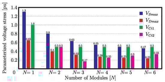
Figure 3.
Parameterized voltage stresses across the semiconductors and capacitors and .
As an advantage, the structure is able to keep the voltage stress on the semiconductors inside a range of values when the input voltage increases just by regulating the number of modules. As can be seen in Figure 4, the four-module converter can operate at twice the input voltage compared to the two-module structure for the same values of output voltage and turns ratio.
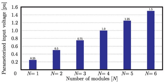
Figure 4.
Parameterized input voltage as a function the number of modules.
Another parameter to be analyzed is the static gain. Figure 5 shows the variation of the static gain as a function of the number of modules. It should be noted that the static gain will decrease when the number of modules increases. Thus, the structure operates as a high step-down voltage regulator with less stresses regarding the duty-cycle, voltage and current.
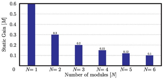
Figure 5.
Static gain as a function the number of modules.
2.1. Modulation Strategy
The proposed converter employs two or more switches; thus, two modulation strategies can be used to generate the command signals. In the first modulation strategy, all switches are turned on at the same time, as seen in Figure 6a. The second modulation strategy is detailed in Figure 6b, and it consists of phase-shift modulation in which the number of modules (N) defines an adequate phase between the carriers () and, consequently, between the gate signals. The phase-shift value is given by
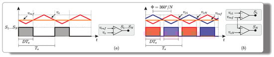
Figure 6.
Gate signal profiles for each modulation strategy: (a) pulses with the same carrier signal; (b) pulses with phase-shifted carriers.
When the first modulation strategy is used (Figure 6a), the proposed converter behaves similarly to the conventional dc–dc SEPIC converter, containing three operating stages in the discontinuous conduction mode (DCM) operation, regardless of the number of modules. The command signals profile of this modulation is called . It was briefly analyzed in [42], and the advantage of the converter using this command signal profile is a reduction in voltage stress across the semiconductors.
The second modulation strategy (Figure 6b) provides an isolated multilevel dc–dc SEPIC, which can operate in three different modes called , and . The operating stages, ideal waveforms, and design equations change in each operation mode. In the DCM operation, the multilevel SEPIC contains 3 operating stages, according to the mode used. The advantages of the multilevel converter are reduced voltage stress across the semiconductors and the smaller volume of the inductors ( and ) and capacitor (). The volume reduction is provided by increasing the operating frequency of these elements, which is proportional to the number of modules used; that is, the volume reduces as the number of modules increases.
In the command signal profile, the converter has an operating restriction related to the maximum duty cycle. In , the converter presents two operating restrictions in terms of duty cycle: one of them is a minimum value, which defines the border between and modes, and the other is a maximum value (), which is the limit where the pulses do not overlap and is the border between modes and . In , the converter also presents two operating restrictions in terms of duty cycle: one is the minimum value defined by and the other is the maximum value, which is the border between the DCM and continuous conduction mode (CCM) operation.
Depending on the design specifications selected, the and restrictions can make applications in these modes unfeasible. In , the duty cycle values can be very small and, consequently, the converter can operate with high-RMS-current values, increasing the losses (reducing the efficiency). For the command signal profile, the range of the duty cycle can be very small, that is, the maximum value of the duty cycle is close to (minimum value).
Considering these factors, the and modes are more applicable in practical experimentation due to the duty cycle ranges. In mode, the converter operates as a multilevel SEPIC, and thus, it was chosen for the study reported in this paper.
2.2. Operation Stages
Operating in DCM with four modules, the converter has twelve operating stages, as seen in Figure 7. However, only the first six operating stages will be described herein, since the next six stages are similar.
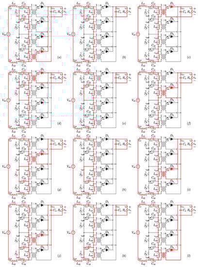
Figure 7.
Operating stages for the command signal profile with four modules: (a) first, (b) second, (c) third, (d) fourth, (e) fifth, (f) sixth, (g) seventh, (h) eighth, (i) ninth, (j) tenth, (k) eleventh, and (l) twelfth.
In the first operating stage (Figure 7a), and are conducting, while , and are turned off. The currents in and are null, since the currents in and reach the same absolute value as the inductor currents in and . Diode is reverse-biased. During this stage, the voltage source , capacitor , and inductors , and supply energy to the inductor , capacitors , and and the load.
When the current in reaches the same absolute value as the inductor currents and , the forward current in is null, initializing the second operating stage (Figure 7b). During this stage, the voltage source and the capacitor supply energy to , , , and , while the capacitor supplies energy to the load.
The third operating stage (Figure 7c) starts when is turned off and, consequently, is forward-biased. In this stage, the voltage source and the inductors , and supply energy to , and the load.
In the fourth operating stage (Figure 7d), is turned on and it conducts together with . Thus, is reverse-biased. The voltage source , , , and supply energy to , , , and the load.
When the current in reaches the same absolute value as the inductor currents of and , the forward current in is null, initializing the fifth operating stage (Figure 7e). During this stage, the voltage source and supply energy to , , , and . The capacitor supplies energy to the load.
The sixth operating stage (Figure 7f) starts when is turned off and, consequently, is forward-biased. In this stage, the voltage source , , and supply energy to , and the load.
3. Theoretical Analysis
The theoretical analysis of the proposed converter operating in DCM is described in this section. All equations are generalized; that is, they are given in relation to the number of modules. Initially, this section presents the analysis in steady state, aiming at the design of the power components, and finally, the dynamic model is presented, which is employed to designed the controller for the closed-loop operation.
The current stress equations (RMS and mean values) were obtained from the waveforms in Figure 8. Every analysis developed in this section is valid when the input inductors are the same value ( = ) as well as the values of the magnetizing inductance of the coupled inductors ( = = … = ).
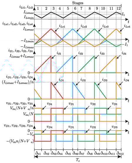
Figure 8.
Ideal waveforms for the command signal profile with four modules.
3.1. Time Intervals
Based on the operating stages and ideal waveforms, the time intervals of each stage are given by
and
where is the input voltage, is the average value of the output voltage, n is the turns ratio, D is the nominal duty cycle and is the switching frequency.
3.2. Static Gain
The static gain is obtained from the equations that represent the output current:
and
3.3. Design of the Inductors and
The input inductances and are defined as a function of the maximum input current ripple (peak-to-peak) during a switching period. Thus, they are given by
where is the ripple current in the input inductors.
The magnetizing inductance ( = = … = ) is chosen to guarantee the DCM operation and is defined from the equation of static gain presented in (12). After some mathematical operations, it is found that
The equations for the RMS current stress in the input () and output () inductors are given by:
where is determined by
3.4. Design of the Capacitors and
The capacitances and are designed from the criteria of maximum voltage ripple (peak-to-peak) in the switching period. The input capacitance will always be designed using the equation given by
where is the ripple voltage in the input capacitors.
When the converter operates with two modules (), the input capacitor is determined from the same equation as , as described in (18). If the converter operates with three () or four () modules, is designed using (18), while and are designed as
The value of the output capacitor is given by
where is the ripple voltage in the output capacitor.
The maximum voltage on the input capacitors is equal to half of the input voltage when the converter operates with two modules (N = 2):
When the converter operates with three (N = 3) or four (N = 4) modules, the maximum voltage across the capacitors and is given by (21), while the maximum voltage on capacitors and is
The maximum voltage on the output capacitor () is equal to the output voltage , which can be written as:
The RMS values of the current in the input capacitors follow the same logic as the maximum voltage; that is, it depends on the number of modules used. Using two modules (N = 2), the RMS values of current in the capacitors and are given by
Operating with three (N = 3) or four (N = 4) modules, the RMS current in capacitors and is obtained from (24), while the RMS current in capacitors and is obtained from
The RMS value of the current in the output capacitor () is obtained with
3.5. Design of the Semiconductors
The switches are chosen from the maximum voltage, described in (1), and the RMS current stress is given by:
The maximum values of the controlled switch currents are determined by:
The diodes are designed from the maximum voltage value and its average current. The maximum voltage across the diodes is presented in (2), while the average value of the current is determined by:
To calculate the theoretical losses in the diodes, the RMS current equation is used, and its value is defined by
The maximum values of the diode currents are determined by:
3.6. Restriction of Operation
The proposed converter in DCM presents up to three operating restrictions for each command signal profile: one related to the critical resistance and the other two associated with the minimum and maximum duty cycle values. It should be noted that only the critical resistances and the maximum duty cycle values of the and modes are related to the DCM operation. Other limits only define the command signal profiles. Table 2 details the expressions of the operating restrictions.
Table 2.
Operating restrictions for , , and .
3.7. Control and Dynamic Model
The proposed SEPIC converter in DCM operation requires control of the output voltage [43]. Therefore, the control strategy shown in Figure 9a is used, which employs a single controller. The equivalent circuit shown in Figure 9b is analyzed to derive the dynamic model of the voltage output as a function of the duty cycle.
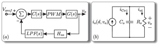
Figure 9.
(a) Block diagram for output voltage control and (b) equivalent circuit for obtaining the dynamic model for output voltage control.
Applying the methodology proposed in [43], the transfer function of the converter to the small signal model is described by
The small signal model for control was validated by numeric simulation. The specifications used are listed in Table 3 and Table 4. During the test, an increase of 2% is applied to the duty cycle at t = 0.092 s and after t = 0.004 s, the value returns to the previous value. The behaviors of the output voltage measured in the converter circuit () and in the proposed dynamic model () in (32) are shown in Figure 10. The proposed model adequately represents the converter in steady and transient states, as shown by the waveforms.
Table 3.
Design Specifications.
Table 4.
List of Components.
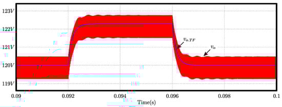
Figure 10.
Numerical validation of the transfer function of the proposed converter.
The use of the proportional–integral (PI) controller is sufficient to maintain the stability of the converter, since the converter operates in DCM and requires only the voltage loop. The PI controller provides null error in steady state for a constant reference. The transfer function of the controller is defined by
4. Prototype and Experimental Results
A prototype of 800 V/120 V/500 W was built to verify the operation and the theoretical analysis of the proposed converter with four modules [], as depicted in Figure 11. The prototype was designed according to the specifications in Table 3, and the main components are listed in Table 4.
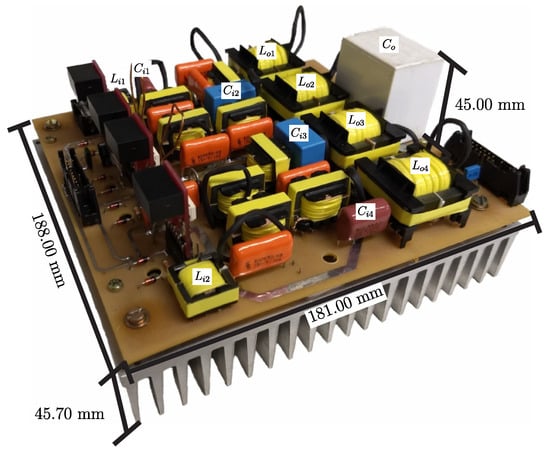
Figure 11.
Photograph of the proposed converter with the regenerative snubber cells.
The experimental results reported herein were obtained in closed-loop operation and at rated power (500 W). Waveforms and curves were measured using the Tektronix DPO 5054 oscilloscope and Yokogawa’s WT500 power analyzer. The leakage inductance values were acquired using an AGILENT 4294A impedance analyzer.
4.1. Design and Prototype Details
As can be seen in Figure 11, four isolated drivers were employed to drive the switches, since they do not have a common reference. To perform the control and generation of command pulses, a digital signal processor (DSP) (model TMS320F28027, Texas Instruments) was used. The controller defined in (33) is designed to allocate the crossover frequency at 100 Hz and the phase margin at 90 degrees, resulting in 30 V (25% of the nominal voltage) overshoot and undershoot for a load increment and load decrement, respectively. In both cases, the settling time was around 3 ms considering the criterion of ±5% of the set point. The Tustin method [44] was used to carry out the discretization of the compensator presented in (33). The sampling frequency used is equal to the switching frequency of the converter.
The command signal profile was chosen for the realization of the prototype due to the duty cycle value. In and with four modules, the duty cycle value is low (0.12). In , the minimum duty cycle value (0.25) was very close to the maximum value (0.273). In , the maximum duty cycle value is 0.25. Therefore, using a duty cycle of 0.24 reduces the maximum and RMS values of the current in the semiconductors and guarantees the DCM operation.
As the proposed converter has high-frequency galvanic isolation, a snubber circuit is needed to prevent overvoltage in the switches, which is caused by the leakage inductance (). Therefore, the passive regenerative snubber circuit proposed in [15] was used. This snubber circuit stores the energy from the leakage inductance, and it transfers part of the energy to the output. In addition, it decreases the switching losses of the switches. As a result, compared to the passive dissipative snubber circuit RCD, the efficiency of the converter increases.
4.2. Experimental Results
The input voltage () and input current () (same current in ) are presented in Figure 12a. Their respective average values are 798.1 V and 728.5 mA. The input current has high-frequency noise in Figure 12a, which is caused by low SNR (signal-to-noise ratio). The measure uses 400 mA per division for a current probe of 30 A. In addition, a high-frequency resonance between the input inductor and input DC source contributes to this noise. Furthermore, these noises do not interfere with the operation of the converter.
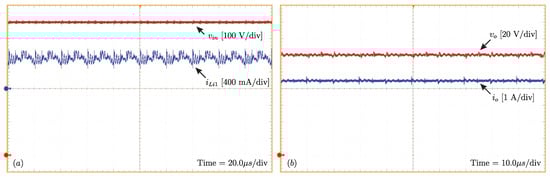
Figure 12.
(a) Input voltage and current and (b) output voltage and current.
Figure 12b shows the experimental waveforms of the output voltage () and output current (), with average values of 121.46 V and 4.403 A, respectively; i.e., the converter is processing approximately 534.79 W.
The voltages across , , , and are shown in Figure 13a. The voltages and currents in and are seen in Figure 13b. The maximum theoretical voltage across the switches follows the relation given in (1), being equal to 440 V. On analyzing the experimental voltages after switching, these values are found to be: 445.61 V, 453.74 V, 459.49 V, and 410 V at , , and , respectively (disregarding the switching phenomena). The maximum voltage values for the switches , , and are: 520 V, 552 V, 548 V and 504 V, respectively, that is, close to the specified value in the snubber circuit design ( = 550 V). These values are analyzed at the instant the switches are turned off. The maximum and RMS values of the currents are 7.87 A and 2.21 A in and 8.03 A and 2.26 A in .
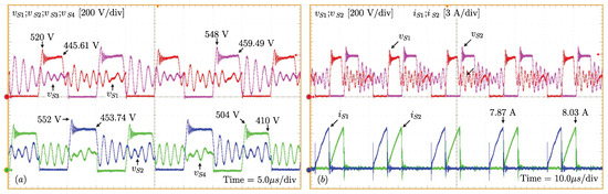
Figure 13.
(a) Voltages across the switches (, , , and ) and (b) voltages and currents in switches and .
DCM operation presents soft commutation naturally when the switches are turned on (current starts from zero each switching period). Additionally, the passive regenerative snubber provides soft commutation when the switches are turned off [15], as verified in Figure 14a. The oscillations in the waveforms refer to the converter discontinuity stage due to DCM operation.
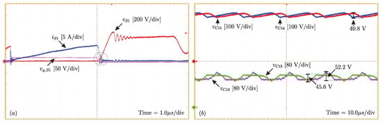
Figure 14.
(a) Details of switching from switch : voltage, current and pulse, and (b) voltage on input capacitors.
The voltage waveforms for , , and can be seen in Figure 14b. The theoretical average voltage on and is equal to half the input voltage (400 V), while for and , it follows the relation (200 V). In the experimental results, the average values for and , respectively, are 401.8 V and 402.2 V, while for and , they are 203.4 V and 207.7 V, respectively.
On analyzing the waveforms for the voltages across , , and (Figure 15a) and the voltages and currents in diodes and (Figure 15b), it can be observed that the maximum voltages values are: −232 V on , −240 V on , −259.2 V on and −241.6 V on . The maximum theoretical voltage value is −220 V, according to (2). The maximum and average currents, respectively, are 14.8 A and 1.18 A in diode and 14.5 A and 1.069 A in . Additionally, the division of the output current between the diodes can be verified through the average current values.
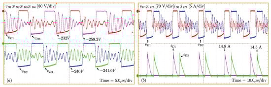
Figure 15.
(a) Voltage across the output diodes (, , and ) and (b) voltage and current in output diodes and .
The dynamic responses applying and removing 50% of the load step are shown in Figure 16a,b. When the load is removed, the overshoot is close to 35 V, while the settling time is approximately 4 ms. When the load is added, the undershoot is approximately 29 V and the settling time is close to 4.85 ms. For the settling time, the criterion of ±5% of the set point is considered. Comparing with the results obtained via design (30 V in both cases) and numerical simulation (34.7 V for overshoot and 27.8 V for undershoot), the overshoot and undershoot values were close. With respect to the settling times, the values were slightly different, with the experimental values being approximately 20% longer.
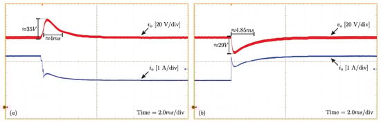
Figure 16.
Transient responses of the output voltage and current to: (a) a decrease and (b) an increase in load.
The efficiency curves (theoretical and experimental) obtained for the proposed converter are shown in Figure 17a. The theoretical peak efficiency value was 93.58% at rated power (500 W), while the maximum experimental efficiency was 94.42% at 538 W.
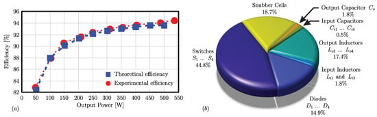
Figure 17.
(a) Efficiency curves for the proposed converter with four modules and (b) distribution of losses for the proposed converter with four modules.
Figure 17b shows the distribution of theoretical losses of the proposed converter (at rated power) with four modules and the regenerative snubber cells. The theoretical analysis shows that most of the losses (59.7%) are concentrated on the semiconductors, while 21.5% relates to passive elements and 18.8% relates to snubber cells. It can be noted that 44.8% (being 43.03% in commutation and 1.77% in conduction) of the losses in semiconductors are in the switches. With an optimized design methodology in the output inductors, the leakage inductance could be lower, which would decrease the losses in the switches and also in the snubber cells. The theoretical losses are calculated based on the methodology from [45,46,47].
4.3. Comparison
In this section, the proposed multilevel SEPIC converter is compared with the ISOP forward [19], ISOP flyback [22] and ISOS flyback [23] converters operating in DCM and using four modules.
A quantitative comparison in relation to the number of components is given in Table 5. Regarding the differences compared with the ISOP forward [19], the proposed converter has seven, three, and four less inductors, capacitors and diodes, respectively. The proposed converter uses an extra inductor compared to the ISOP flyback [22], but it presents three less capacitors. In relation to the ISOS flyback [23], the proposed converter employs an extra inductor; however, it has three, four, and eight less capacitors, switches and diodes, respectively. It should also be noted that the proposed multilevel SEPIC converter presented in Figure 2c has two inductors at the input ( and ) that can be integrated into a single inductor, and thus, one of them does not count as an extra element in the quantitative analysis.
Table 5.
Quantitative Analysis.
The qualitative analysis is reported in Table 6. The values are given in pu (per-unit), each variable being normalized by the respective value in the proposed converter. In relation to the ISOP forward [19], the voltage stresses on the semiconductors are similar for the design specifications used, while the current stresses on the magnetizing inductances and output capacitor are higher and those on other components are lower or equal. In comparison with the ISOP flyback [22], the voltage stresses on the semiconductors are also the same. The current stresses on the input capacitors and the output capacitor are greater. In the rest of the elements, the current stresses are similar. The ISOS flyback described in [23] presents reduced voltage stress across the semiconductors compared to the proposed converter. On the other hand, the current stresses in the magnetizing inductances are doubled, while the average current at the output diodes is four times greater. The current stresses on the input capacitors are lesser.
Table 6.
Qualitative Analysis.
Table 7 presents a comparison of the experimental parameters of the proposed converter with other solutions. It should be noted that the proposed converter and [19] have a continuous current at the converter input with low ripple, while the converters in [22,23] have pulsed current with high ripple. In relation to the efficiency values, it can be observed that the converters present similar efficiencies, with a difference of 1%, except for the converter presented in [19], which does not show experimental efficiency data. The proposed converter and the converters proposed in [19,23] have lower gains compared to the converter from [22]. Additionally, the proposed converter and proposed in [23] present higher input voltage levels. In relation to the output power, the proposed converter and [19] were tested in similar power, while the converter from [22] operated with lower power level and the converter in [23] operated with higher power level.
Table 7.
Experimental comparison of proposed converter and other solutions.
In conclusion, the proposed converter has voltage stresses on semiconductors either equal to or similar to the structures presented in [19,22]. The current stresses on the elements of the proposed converter are also similar in comparison to [19,22,23]. The main contribution highlighted by the prototype is a reduction in the number of power components when compared to the structures presented in [19,22,23]. In additional, the proposed converter features continuous current at the input with low ripple, while the converters shown in [22,23] have pulsed current at the input with high ripple.
5. Conclusions
In this paper, a multilevel SEPIC converter in DCM was proposed, which is obtained from the integration of N conventional SEPIC converters. This integration reduces the voltage stress across the semiconductors and the division of the current stress in the output diodes, since the outputs are connected in parallel. The other components remain with the same current stress, regardless of the number of modules used. The voltage-stress reduction on the switches is the main contribution in relation to the conventional SEPIC, and this feature means that the SEPIC-converter family can be applied with higher input voltages (for instance, the converter can operate in dc microgrids with input voltage at 800 V).
The proposed converter employs N switches, and two different modulation strategies can be used to generate the command signals. The most advantageous modulation strategy is that with the command signals phase-shifted by degrees, because a multilevel converter is obtained, reducing the volume of the input inductors ( and ) and the output capacitor (). Another advantage of using the phase-shifted signals ( and ) is the reduction of the maximum and RMS values of the current in the output capacitor.
The experimental results obtained with the four-module 500 W prototype corroborated the results of the theoretical analysis for the proposed converter. A passive regenerative snubber was added to the circuit due to the leakage inductance of the coupled inductors. The maximum efficiency obtained was 94.42% at rated power (538 W). This efficiency value can be also increased with an optimized design of the output inductors.
In addition, the proposed multilevel dc–dc SEPIC converter can be used for higher voltages using components from lower voltage rates, and it may be applied in a dc microgrid for different levels of the input voltage bus simply by adjusting the number of modules.
Author Contributions
Conceptualization, M.V.M.E., T.B.L. and C.H.I.F.; software, M.V.M.E.; validation, M.V.M.E.; formal analysis, M.V.M.E., T.B.L. and C.H.I.F.; investigation, M.V.M.E., T.B.L. and C.H.I.F.; data curation, M.V.M.E.; writing—original draft preparation, M.V.M.E.; writing—review and editing, T.B.L. and C.H.I.F.; supervision, T.B.L. and C.H.I.F.; project administration, T.B.L. and C.H.I.F.; funding acquisition, C.H.I.F. All authors have read and agreed to the published version of the manuscript.
Funding
This research was funded by Coordination for the Improvement of Higher Education Personnel (CAPES)—Financing Code 001.
Data Availability Statement
No new data were created or analyzed in this study. Data sharing is not applicable to this paper.
Acknowledgments
The authors would like to thank CAPES for their contribution to this work in the form of a grant provided to Marcos Vinicius Mosconi Ewerling.
Conflicts of Interest
The authors declare no conflict of interest.
References
- Rahbar, K.; Xu, J.; Zhang, R. Real-time energy storage management for renewable integration in microgrid: An off-line optimization approach. IEEE Trans. Smart Grid 2014, 6, 124–134. [Google Scholar] [CrossRef]
- Mariscotti, A. Power quality phenomena, standards, and proposed metrics for dc grids. Energies 2021, 14, 6453. [Google Scholar] [CrossRef]
- Rahbar, K.; Chai, C.C.; Zhang, R. Energy cooperation optimization in microgrids with renewable energy integration. IEEE Trans. Smart Grid 2016, 9, 1482–1493. [Google Scholar] [CrossRef]
- Anand, S.; Fernandes, B. Optimal voltage level for DC microgrids. In Proceedings of the IECON 2010-36th Annual Conference on IEEE Industrial Electronics Society, Glendale, AZ, USA, 7–10 November 2010; pp. 3034–3039. [Google Scholar]
- Yu, X.; Jin, K.; Liu, Z. Capacitor voltage control strategy for half-bridge three-level DC/DC converter. IEEE Trans. Power Electron. 2013, 29, 1557–1561. [Google Scholar] [CrossRef]
- Jung, C. Power Up with 800-V Systems: The benefits of upgrading voltage power for battery-electric passenger vehicles. IEEE Electrif. Mag. 2017, 5, 53–58. [Google Scholar] [CrossRef]
- Qian, W.; Lu, J.; Bai, H.; Averitt, S. Hard-switching 650-V GaN HEMTs in an 800-V dc-grid system with no-diode-clamping active-balancing three-level topology. IEEE J. Emerg. Sel. Top. Power Electron. 2018, 7, 1060–1070. [Google Scholar] [CrossRef]
- Nilsson, D.; Sannino, A. Efficiency analysis of low-and medium-voltage DC distribution systems. In Proceedings of the IEEE Power Engineering Society General Meeting, Denver, CO, USA, 6–10 June 2004; pp. 2315–2321. [Google Scholar]
- Sannino, A.; Postiglione, G.; Bollen, M. Feasibility of a DC network for commercial facilities. IEEE Trans. Ind. Appl. 2003, 39, 1499–1507. [Google Scholar] [CrossRef]
- Salomonsson, D.; Sannino, A. Low-voltage DC distribution system for commercial power systems with sensitive electronic loads. IEEE Trans. Power Deliv. 2007, 22, 1620–1627. [Google Scholar] [CrossRef]
- Kyriakou, D.G.; Kanellos, F.D. Optimal Operation of Microgrids Comprising Large Building Prosumers and Plug-in Electric Vehicles Integrated into Active Distribution Networks. Energies 2022, 15, 6182. [Google Scholar] [CrossRef]
- Amanci, A.Z.; Ruda, H.E.; Dawson, F.P. Galvanic isolation for high-frequency applications using an integrated dielectric structure. IEEE Trans. Power Electron. 2015, 31, 5797–5804. [Google Scholar] [CrossRef]
- Jinno, M. Efficiency improvement for SR forward converters with LC snubber. IEEE Trans. Power Electron. 2001, 16, 812–820. [Google Scholar] [CrossRef]
- Kasasbeh, A.; Kelleci, B.; Ozturk, S.B.; Aksoz, A.; Hegazy, O. SEPIC Converter with an LC Regenerative Snubber for EV Applications. Energies 2020, 13, 5765. [Google Scholar] [CrossRef]
- Tibola, G.; Lemmen, E.; Duarte, J.L.; Barbi, I. Passive regenerative and dissipative snubber cells for isolated SEPIC converters: Analysis, design, and comparison. IEEE Trans. Power Electron. 2017, 32, 9210–9222. [Google Scholar] [CrossRef]
- Kanamarlapudi, V.R.K.; Wang, B.; Kandasamy, N.K.; So, P.L. A New ZVS Full-Bridge DC–DC Converter for Battery Charging With Reduced Losses Over Full-Load Range. IEEE Trans. Ind. Appl. 2018, 54, 571–579. [Google Scholar] [CrossRef]
- Zhang, S.; Wu, X. Low Common Mode Noise Half-Bridge LLC dc-dc Converter With an Asymmetric Center Tapped Rectifier. IEEE Trans. Power Electron. 2019, 34, 1032–1037. [Google Scholar] [CrossRef]
- Rehlaender, P.; Schafmeister, F.; Böcker, J. Interleaved Single-Stage LLC Converter Design Utilizing Half- and Full-Bridge Configurations for Wide Voltage Transfer Ratio Applications. IEEE Trans. Power Electron. 2021, 36, 10065–10080. [Google Scholar] [CrossRef]
- Giri, R.; Choudhary, V.; Ayyanar, R.; Mohan, N. Common-duty-ratio control of input-series connected modular DC-DC converters with active input voltage and load-current sharing. IEEE Trans. Ind. Appl. 2006, 42, 1101–1111. [Google Scholar] [CrossRef]
- Qu, L.; Zhang, D.; Bao, Z. Output current-differential control scheme for input-series–output-parallel-connected modular DC–DC converters. IEEE Trans. Power Electron. 2016, 32, 5699–5711. [Google Scholar] [CrossRef]
- Qu, L.; Zhang, D.; Zhang, B. Input voltage sharing control scheme for input series and output parallel connected DC–DC converters based on peak current control. IEEE Trans. Ind. Electron. 2018, 66, 429–439. [Google Scholar] [CrossRef]
- Fuerback, V.B.; Pagliosa, M.A.; Dall’Asta, M.S.; Lazzarin, T.B. Modular ISOP Flyback converter: Analysis of auto-balancing mechanism in steady state. In Proceedings of the 2017 IEEE 8th International Symposium on Power Electronics for Distributed Generation Systems (PEDG), Florianopolis, Brazil, 17–20 April 2017; pp. 1–6. [Google Scholar]
- Pagliosa, M.A.; Lazzarin, T.B.; Barbi, I. Modular Two-Switch Flyback Converter and Analysis of Voltage-Balancing Mechanism for Input-Series and Output-Series Connection. IEEE Trans. Power Electron. 2019, 34, 8317–8328. [Google Scholar] [CrossRef]
- Giri, R.; Ayyanar, R.; Ledezma, E. Input-series and output-series connected modular DC-DC converters with active input voltage and output voltage sharing. In Proceedings of the 2004 IEEE 9th Applied Power Electronics Conference and Exposition (APEC), Anaheim, CA, USA, 22–26 February 2004; Volume 3, pp. 1751–1756. [Google Scholar]
- Chen, J.; Wang, C.; Li, J.; Jiang, C.; Duan, C. An Input-Parallel–Output-Series Multilevel Boost Converter With a Uniform Voltage- Balance Control Strategy. IEEE J. Emerg. Sel. Top. Power Electron. 2019, 7, 2147–2157. [Google Scholar] [CrossRef]
- Fuerback, V.B.; Dall’Asta, M.S.; Pagliosa, M.A.; Lazzarin, T.B. Analysis of modular DCM Flyback converters in input parallel connections with parametric mismatches. Eletrônica Potência SOBRAEP 2019, 24, 225–234. [Google Scholar] [CrossRef]
- Chen, Z.; Liu, B.; Yang, Y.; Davari, P.; Wang, H. Bridgeless PFC Topology Simplification and Design for Performance Benchmarking. IEEE Trans. Power Electron. 2021, 36, 5398–5414. [Google Scholar] [CrossRef]
- Golbon, N.; Ghodousipour, F.; Moschopoulos, G. A DC-DC converter with stacked flyback converters. In Proceedings of the 2013 IEEE Energy Conversion Congress and Exposition, Denver, CO, USA, 15–19 September 2013; pp. 4894–4899. [Google Scholar]
- Zhou, Z.; Li, L. Isolated SEPIC three-level DC-DC converter. In Proceedings of the 2011 6th IEEE Conference on Industrial Electronics and Applications, Beijing, China, 21–23 June 2011; pp. 2162–2165. [Google Scholar]
- Andrade, A.M.S.S.; da Silva Martins, M.L. Quadratic-boost with stacked zeta converter for high voltage gain applications. IEEE J. Emerg. Sel. Top. Power Electron. 2017, 5, 1787–1796. [Google Scholar] [CrossRef]
- Do, H.L. Soft-switching SEPIC converter with ripple-free input current. IEEE Trans. Power Electron. 2011, 27, 2879–2887. [Google Scholar] [CrossRef]
- Lee, S.W.; Do, H.L. Isolated SEPIC DC–DC converter with ripple-free input current and lossless snubber. IEEE Trans. Ind. Electron. 2017, 65, 1254–1262. [Google Scholar] [CrossRef]
- Nasr Esfahani, F.; Darwish, A.; Massoud, A. PV/Battery Grid Integration Using a Modular Multilevel Isolated SEPIC-Based Converter. Energies 2022, 15, 5462. [Google Scholar] [CrossRef]
- Anuradha, C.; Chellammal, N.; Saquib Maqsood, M.; Vijayalakshmi, S. Design and analysis of non-isolated three-port SEPIC converter for integrating renewable energy sources. Energies 2019, 12, 221. [Google Scholar] [CrossRef]
- Blinov, A.; Verbytskyi, I.; Zinchenko, D.; Vinnikov, D.; Galkin, I. Modular battery charger for light electric vehicles. Energies 2020, 13, 774. [Google Scholar] [CrossRef]
- Chiu, H.J.; Lo, Y.K.; Chen, J.T.; Cheng, S.J.; Lin, C.Y.; Mou, S.C. A high-efficiency dimmable LED driver for low-power lighting applications. IEEE Trans. Ind. Electron. 2009, 57, 735–743. [Google Scholar] [CrossRef]
- Burgardt, I.; Junior, E.A.; Font, C.H.I.; Nascimento, C.B. Dimmable flicker-free power LEDs lighting system based on a SEPIC rectifier using a regenerative snubber. IET Power Electron. 2016, 9, 891–899. [Google Scholar] [CrossRef]
- Simonetti, D.S.L.; Sebastian, J.; Uceda, J. The discontinuous conduction mode Sepic and Cuk power factor preregulators: Analysis and design. IEEE Trans. Ind. Electron. 1997, 44, 630–637. [Google Scholar] [CrossRef]
- Kim, J.; Han, S.; Cho, W.; Cho, Y.; Koh, H. Design and analysis of a repetitive current controller for a single-phase bridgeless SEPIC PFC converter. Energies 2018, 12, 131. [Google Scholar] [CrossRef]
- Freitas, T.; Caliman, J.; Menegáz, P.; dos Santos, W.; Simonetti, D. A DCM Single-Controlled Three-Phase SEPIC-Type Rectifier. Energies 2021, 14, 256. [Google Scholar] [CrossRef]
- Yang, J.W.; Do, H.L. Bridgeless SEPIC converter with a ripple-free input current. IEEE Trans. Power Electron. 2012, 28, 3388–3394. [Google Scholar] [CrossRef]
- Ewerling, M.V.M.; Lazzarin, T.B.; Illa Font, C.H. Proposal of an Isolated Two-Switch DC-DC SEPIC Converter. In Proceedings of the 15th Brazilian Power Electronics Conference and 5th IEEE Southern Power Electronics Conference (COBEP/SPEC), Santos, Brazil, 1–4 December 2019; pp. 1–6. [Google Scholar]
- Costa, P.J.S.; Font, C.H.I.; Lazzarin, T.B. A family of single-phase voltage-doubler high-power-factor SEPIC rectifiers operating in DCM. IEEE Trans. Power Electron. 2016, 32, 4279–4290. [Google Scholar] [CrossRef]
- Buso, S.; Mattavelli, P. Digital Control in Power Electronics; Hudgins, J., Ed.; Morgan & Claypool Publishers: Seattle, WA, USA, 2006. [Google Scholar]
- Weitzel, C.; Palmour, J.; Carter, C.; Moore, K.; Nordquist, K.; Allen, S.; Thero, C.; Bhatnagar, M. Silicon carbide high-power devices. IEEE Trans. Electron. Devices 1996, 43, 1732–1741. [Google Scholar] [CrossRef]
- Graovac, D.; Purschel, M.; Kiep, A. MOSFET power losses calculation using the data-sheet parameters. Infineon Appl. Note 2006, 1, 1–23. [Google Scholar]
- Papamanolis, P.; Guillod, T.; Krismer, F.; Kolar, J.W. Minimum Loss Operation and Optimal Design of High-Frequency Inductors for Defined Core and Litz Wire. IEEE Open J. Power Electron. 2020, 1, 469–487. [Google Scholar] [CrossRef]


Publisher’s Note: MDPI stays neutral with regard to jurisdictional claims in published maps and institutional affiliations. |
© 2022 by the authors. Licensee MDPI, Basel, Switzerland. This article is an open access article distributed under the terms and conditions of the Creative Commons Attribution (CC BY) license (https://creativecommons.org/licenses/by/4.0/).