1. Introduction
Since the LLC resonant converter was proposed, it has been quickly applied to all walks of life because of its high efficiency and high power-density [
1].
Figure 1 shows the circuit topology of the LLC resonant converter. The LLC resonant converter utilizes the characteristics of the resonant element to control the magnitude of the output voltage by changing the frequency of the square wave voltage input to the tank circuit. The parameters of the resonant element determine the gain curve of the converter under frequency modulation (FM) control. When the value of the magnetic inductance
Lm is smaller, the gain range of the resonant converter is wider and the turn-off loss and conduction loss introduced into the circuit will be larger [
2,
3]; the two requirements of high efficiency and wide gain are difficult to coexist at the same time.
Using FM control alone, the output voltage of the converter decreases as the switching frequency increases. However, a too-high switching frequency will not only increase the loss of the circuit but also make the selection of the device more stringent. Some scholars have proposed a hybrid control strategy of frequency modulation combined with phase shifting [
4,
5]. When the switching frequency increases to the resonant frequency, the switching frequency is fixed and the output voltage is changed by controlling the phase shifting angle of the switch. The minimum phase shift angle can be reduced to 0, thus expanding the output voltage range of the resonant converter.
A too-small phase shift angle will also increase losses in the circuit. Reference [
6] proposed a variable mode control strategy to achieve the purpose of wide output. In this control mode, when the input voltage gradually increases, the circuit will work in three operating modes in turn: full-bridge frequency modulation, full-bridge phase shift and half-bridge frequency modulation. This control strategy has been able to provide a considerable gain range, but when the required gain range is further expanded, it will be required to continue to increase the switching frequency, or to redesign the turns ratio of the transformer [
7,
8].
To further widen the output voltage range of the resonant converter, a novel wide-output resonant converter is proposed here.
Figure 2 shows the main circuit part of the converter, and Q
1–Q
6 are active switches that constitute three inverter arms. The diodes D
1–D
6 are the body diodes of Q
1–Q
6, and
C1–C6 are the parasitic capacitances of each active switch, respectively. There are two transformers, T
1 and T
2, with the same transformation ratio in the circuit. On the primary side of the transformer, there are resonant capacitors
Cr1,
Cr2, resonant inductors
Lr1,
Lr2 and excitation inductors
Lm1,
Lm2. The corresponding resonant parameters in the two tank circuits are the same. On the secondary side of the transformer, D
R1–D
R6 form a new series-parallel self-adjusting rectifier structure.
2. Analysis of Each Working Mode of the Converter
In the new resonant converter proposed in this paper, according to the structural difference between the full-bridge and the half-bridge of the inverter unit and the difference in frequency modulation and phase shift in the control methods, the new resonant converter has four operating modes, followed by the full-bridge frequency modulation mode, full-bridge phase-shift mode, half-bridge FM mode and half-bridge phase-shift mode. Each operating mode has its own corresponding gain range.
2.1. Full-Bridge FM Mode
In the full-bridge FM mode, the driving waveforms of switches Q
1, Q
4 and Q
5 are the same and the driving waveforms of switches Q
2, Q
3 and Q
6 are also the same. The two sets of switches are complementarily turned on, providing square wave voltages with the same phase and an amplitude of ±
Vin for the two tank circuits. The rectified currents output by the secondary sides of the two transformers are also of the same phase and the same amplitude, so DR
3 and DR
4 in the rectifier bridge do not work within one switching cycle. In the full-bridge FM mode, the main circuit can be equivalent to two LLC resonant converters, the input terminals are connected in parallel and the output terminals are connected in series, as shown in
Figure 3. The gain range of the resonant converter in this mode is twice that of a single full-bridge LLC resonant converter under FM control. The main waveform diagram in full-bridge FM mode is shown in
Figure 4.
2.2. Full-Bridge Phase Shift Mode
In the full-bridge phase-shift mode, the driving waveforms of the inverter bridge arm composed of switches Q
1 and Q
2 and the inverter bridge arms composed of switches Q
5 and Q
6 have the same timing sequence, and lag behind those composed of switches Q
3 and Q
4. A phase shift angle is generated for phase shift control and changes the size of the output voltage. At this time, the input square wave voltages of the two tank circuits are also the same, and the equivalent circuit diagram of the main circuit is the same as the equivalent circuit diagram in the full-bridge frequency modulation mode. The gain of the circuit is twice that of a single full-bridge LLC resonant circuit under phase-shift control. The main waveforms in full-bridge phase-shift mode are shown in
Figure 5.
2.3. Half-Bridge FM Mode
In the half-bridge frequency modulation mode, the switch Q
4 is kept on, the switch Q
3 is kept off and the remaining four switches work in the frequency modulation control. The input square wave voltages of the two tank circuits are still the same in amplitude and phase, so the secondary side rectifier diodes D
R3 and D
R4 do not work all the time. The main circuit can be equivalent to two half-bridge LLC resonant circuits with inputs in parallel and outputs in series, as shown in
Figure 6. In the half-bridge FM mode, the effective value of the input voltage of the tank circuit is half that of the full-bridge FM mode in one switching cycle, and its gain is naturally reduced to 1/2. The main waveforms in the half-bridge FM mode are similar to those in the full-bridge FM mode.
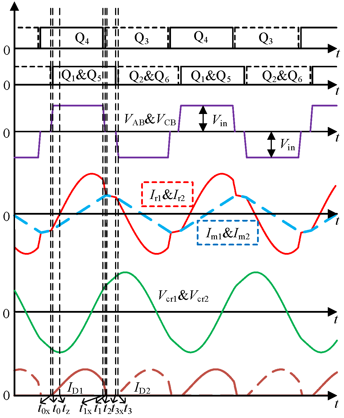
2.4. Half-Bridge Phase Shift Mode
In the half-bridge phase-shift mode, the switch Q
4 is kept on and the switch Q
3 is kept off. A certain phase angle is generated between the inverter bridge arm composed of switches Q
1 and Q
2 and the drive waveform of the inverter bridge arm composed of switches Q
5 and Q
6. At this time, the equivalent circuit diagram of the main circuit is shown in
Figure 7. Although the input terminal can still be regarded as the input of two half-bridge LLC resonant converters in parallel, the phase of the input square wave voltage
VAB and
VCB of the two tank circuits is no longer consistent and the output of the transformer is not always in series. The size of the phase shift angle determines the time for the output of the two transformer secondary sides to work in series and the time for a single transformer to independently transmit energy in half a switching cycle, and then controls the equivalent turns ratio of the transformer to change the output voltage. The main working waveform diagram in the half-bridge phase-shift mode is shown in
Figure 8.
The specific working states of full-bridge LLC resonant converters under frequency modulation control or phase-shift control and half-bridge LLC resonant converters under frequency modulation control have been described in detail in much of the literature, so only the half-bridge phase-shift control mode is analyzed here.
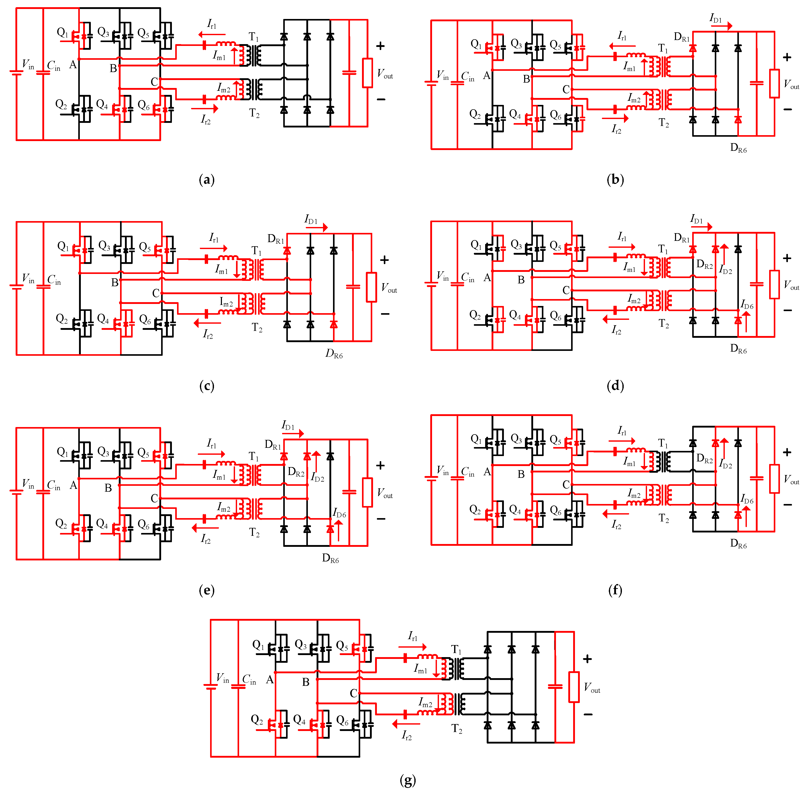
Before time
t0x (
Figure 9a), the switches Q
1 and Q
6 are turned on, and Q
2 and Q
5 are turned off. The voltage at the input terminal of resonance tank 1 is
VAB =
Vin, and the voltage at the input terminal of resonance tank 2 is
VCB = 0. The resonant current is equal to the value of the excitation current, there is no energy transfer on the primary and secondary sides and the six diodes on the secondary side are all turned off.
In the [
t0x,
t0] stage (
Figure 9b) at
t0x, the switch Q
6 is turned off and the resonant current
Ir2 charges the capacitor
C6 and discharges the capacitor
C5 until the capacitor voltage across
C6 is charged to the input voltage
Vin, and
C5 is also discharged completely; the switch tube Q
5 is ready for zero-voltage turn-on. At this time, the resonant current
Ir2 continues to flow through the body diode D
2 of Q
6. The switch on bridge arm 3 has no action.
The input terminal voltage VCB of tank circuit 2 increases from 0, and the resonant current Ir2 starts to rise. Because the current difference between the resonant current and the excitation current is generated, the energy is transferred from the primary side of the transformer to the secondary side, the diodes D1 and D6 are turned on, the excitation inductances Lm1 and Lm2 are both clamped by nVout/2 and the excitation current increases linearly. Resonant current Ir2 of tank circuit 1 also begins to rise and the outputs of the two transformers are connected in series.
- 3.
[
t0,
t1x] stage (
Figure 9c) at
t0, the switch Q
5 is turned on at zero voltage, the voltage
VCB =
Vin is applied to the input of tank circuit 2, the inputs of the two tank circuits are connected in parallel, and the power supply charges the resonant capacitor. The resonant currents
Ir1 and
Ir2 gradually increase from negative values to 0 and keep rising, and the primary side continues to transfer energy to the secondary side. The expressions of
vcr1,
vcr2,
ir1,
ir2,
im1,
im2 in this stage are as follows.
- 4.
[
t1x,
t1] stage (
Figure 9d) at
t1x, the switch Q
1 is turned off and the resonant current
Ir1 charges the capacitor
C1 and discharges the capacitor
C2 until the capacitor voltage across
C1 is charged to the input voltage
Vin, and
C2 is also discharged, the switch Q
2 is ready for zero-voltage turn-on, and the resonant current
Ir1 continues to flow through the body diode D
1 of Q
1. The switch on bridge arm 3 has no action.
Because the switch Q1 is turned off, the input voltage VAB of tank circuit 1 starts to drop from Vin and the resonant current Ir1 also starts to drop rapidly. Although the resonant current Ir2 in tank circuit 2 also decreases at this time, the VCB does not change, so the resonant current Ir2 decreases at a lower speed than Ir1. The difference in the descending slopes of the two resonant currents makes the rectified current transmitted by tank circuit 1 to the secondary side of the transformer smaller than that of tank circuit 2. To satisfy Kirchhoff’s current law, the rectifier diode DR3 on the secondary side is turned on to play a shunt. When DR3 is turned on, the secondary side of tank circuit 1 is short-circuited, the clamping voltage across the excitation inductance Lm1 drops from nVout/2 to 0, and the excitation current Im1 no longer increases. The clamping voltage across the excitation inductor Lm2 rises from nVout/2 to nVout, and the excitation current Im2 rises faster. The input of tank circuit 2 does not change, but the clamping voltage of Lm2 increases, which explains why Ir2 also decreases.
- 5.
In the [
t1,
t2] stage (
Figure 9e) at the time of
t1, switch Q
2 is turned on at zero voltage,
VAB = 0 and resonance tanks 1 and 2 continue to resonate. However, because the output of tank circuit 1 is short-circuited, only tank circuit 2 transmits energy to the secondary side during this period. The expressions of
vcr1,
vcr2,
ir1,
ir2,
im1,
im2 in this stage are as follows.
- 6.
[
t2,
t3] stage (
Figure 9f) at time
t2, the resonant current
Ir1 in tank circuit 1 is equal to the excitation current
Im1, the excitation inductance
Lm1 participates in the resonance, and rectifier diode D
1 is turned off at zero current. Tank circuit 2 is still in the resonant state, and all the currents transmitted by the secondary side of the transformer are transmitted to the load side through the diodes D
2 and D
6. The expressions of
vcr1,
vcr2,
ir1,
ir2,
im1,
im2 in this stage are as follows.
The expression of each state variable in resonance tank 2 is consistent with the previous stage.
- 7.
In the [
t3,
t4] stage (
Figure 9g), resonant current
Ir2 in tank circuit 2 at the time of
t3 is equal to the excitation current
Im2, and the excitation inductance
Lm2 participates in the resonance. So far, the two transformers are cut off from the secondary side. The primary and secondary sides of the circuit no longer have energy transfer and the load is powered by the output capacitor.
The expression of each state variable in resonance tank 1 is consistent with the previous stage.
Through the above analysis, it can be obtained that in the half-bridge phase-shift mode, the active switch in the topology has zero-voltage turn-on capability, and the rectifier diode can achieve zero-current turn-off.
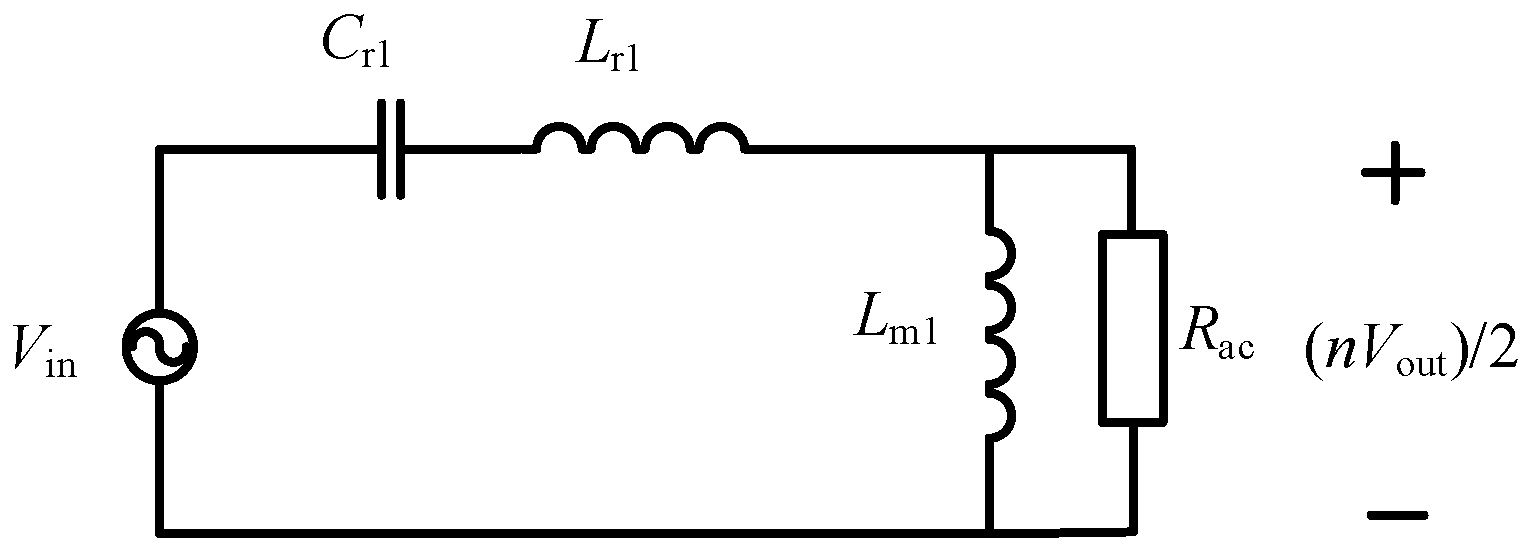
3. Gain Analysis
Among the gain analysis methods of resonant converters, the most commonly used is the fundamental wave analysis method (first harmonic approximation, FHA) [
9,
10]. In FHA, the input square wave voltage of the tank circuit is approximately regarded as its fundamental wave component and its higher harmonics are ignored, and the load R
L is converted to the primary side
Rac = 4
n2RL/π
2 under the assumption that the secondary side rectified current is a sine wave, so that the tank circuit in the main circuit is transformed into an equivalent model as shown in
Figure 10.
According to the equivalent circuit diagram, the analytical expressions of the gain of the converter in the full-bridge FM mode and the half-bridge FM mode can be listed.
Half-bridge FM:
where
Q =
Zr/
Rac represents the quality factor,
h =
Lm/
Lr represents the inductance ratio,
fn =
fs/
fr represents the normalized frequency,
fs is the switching frequency and
fr is the resonant frequency.
Through the analytical expression of gain, we can draw the DC gain curves in full-bridge FM mode and half-bridge FM mode, as shown in
Figure 11 and
Figure 12, respectively.
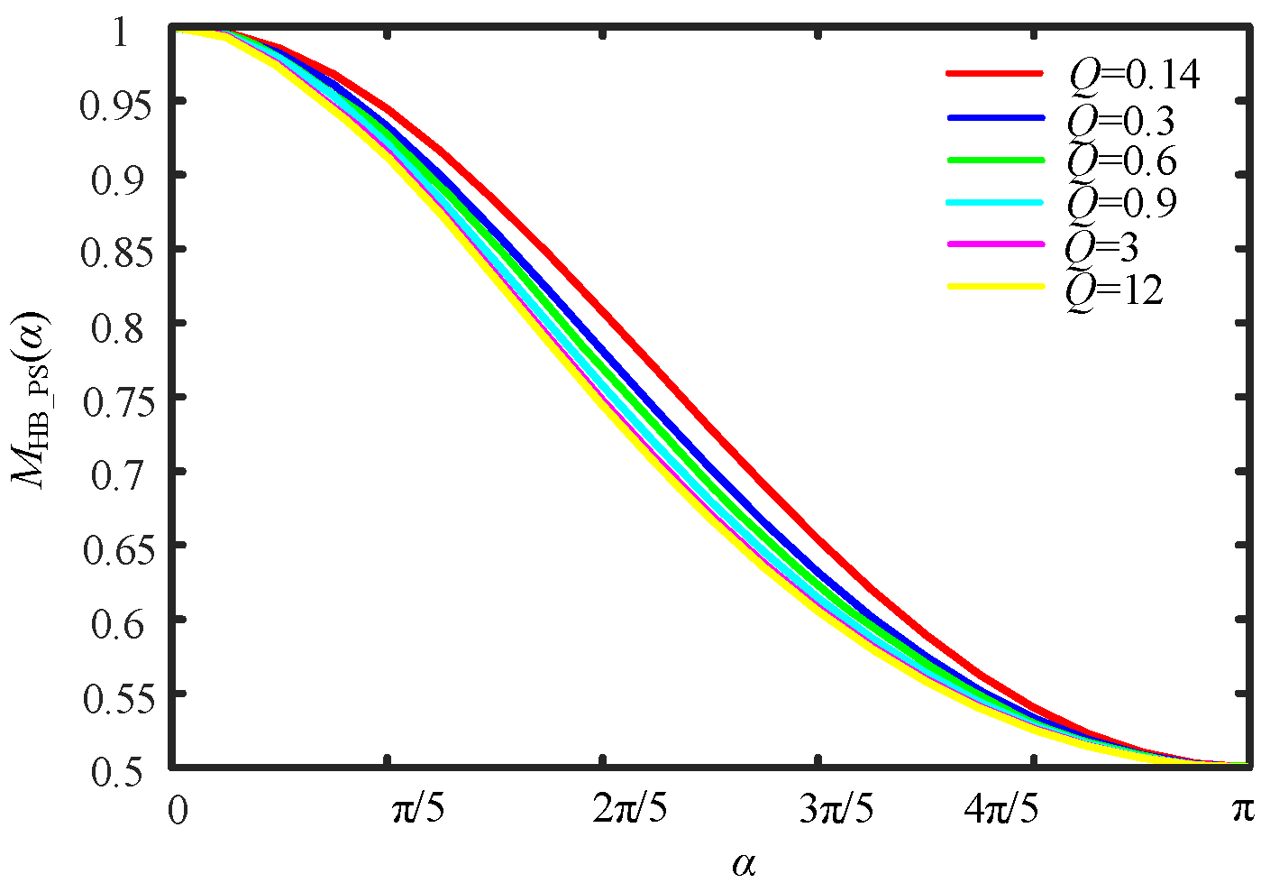
When the resonant converter adopts the fixed-frequency and phase-shift control, the harmonic content increases, and the continuous use of the fundamental wave analysis method will cause a large error. Therefore, in the gain analysis of the full-bridge phase-shift mode and the half-bridge phase-shift mode, the time domain analysis method is used to write the time domain expressions of each state quantity in the tank circuit in different stages, and the calculation software can be used to draw the DC gain curves of the full-bridge phase-shift mode and the half-bridge phase-shift mode are shown in
Figure 13 and
Figure 14.
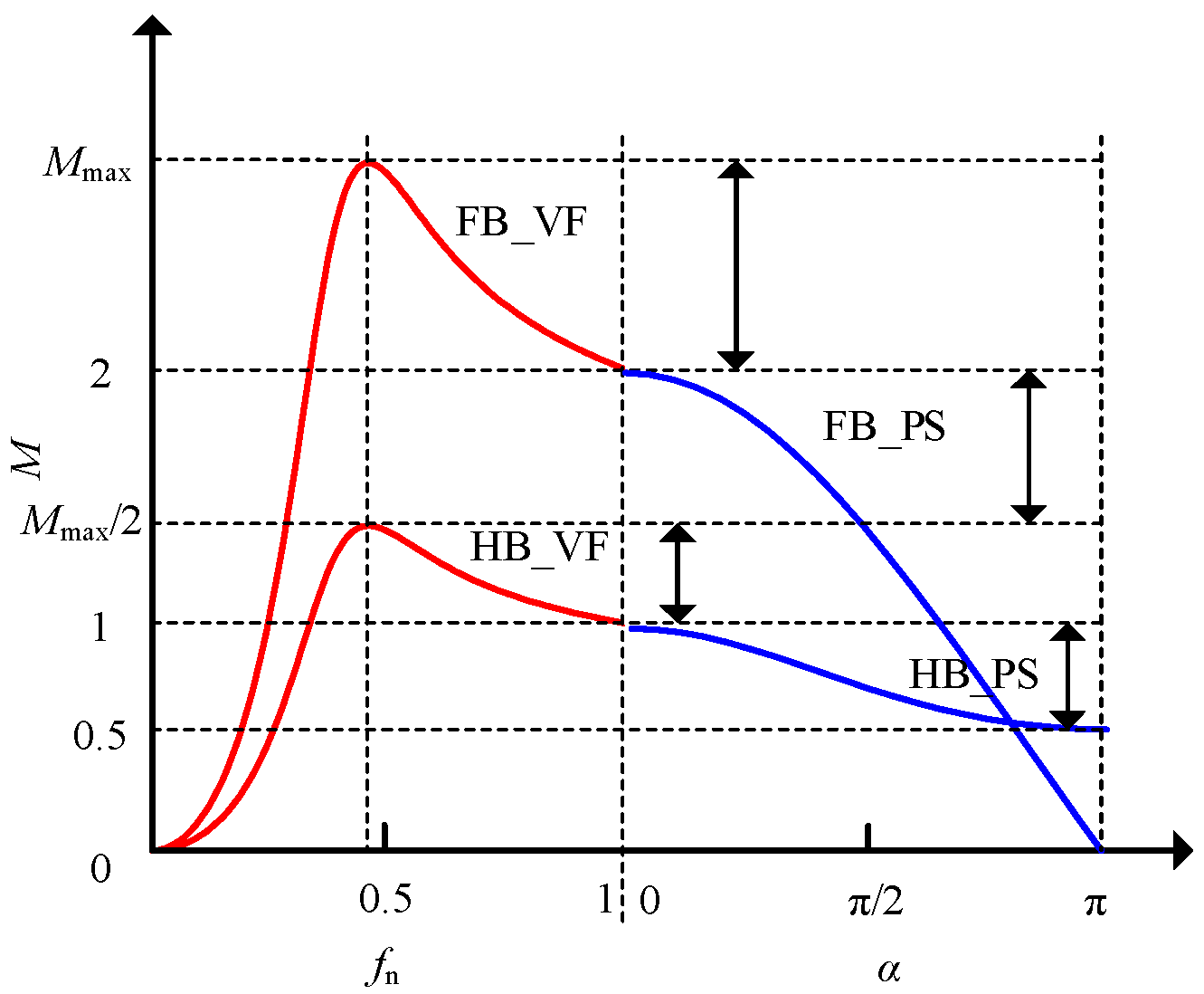
When the circuit works in full-bridge FM or half-bridge FM mode, the switching frequency
fs always works below the resonant frequency
fr. When
fs >
fr, the rectifier diode on the secondary side of the transformer loses the ability to turn off zero current. In the full-bridge phase-shift and half-bridge phase-shift modes, the switching frequency
fs =
fr is set to maintain the high efficiency of the efficient transmission. Combined with the above gain analysis, the overall gain curve of the multi-mode switching wide-output resonant converter proposed in this paper is obtained, as shown in
Figure 15.
4. Experiment Verifications
To verify the wide output capability and soft switching characteristics of the novel resonant converter proposed in this paper, a 100 W experimental prototype was built.
Table 1 lists the main parameters of the experimental prototype.
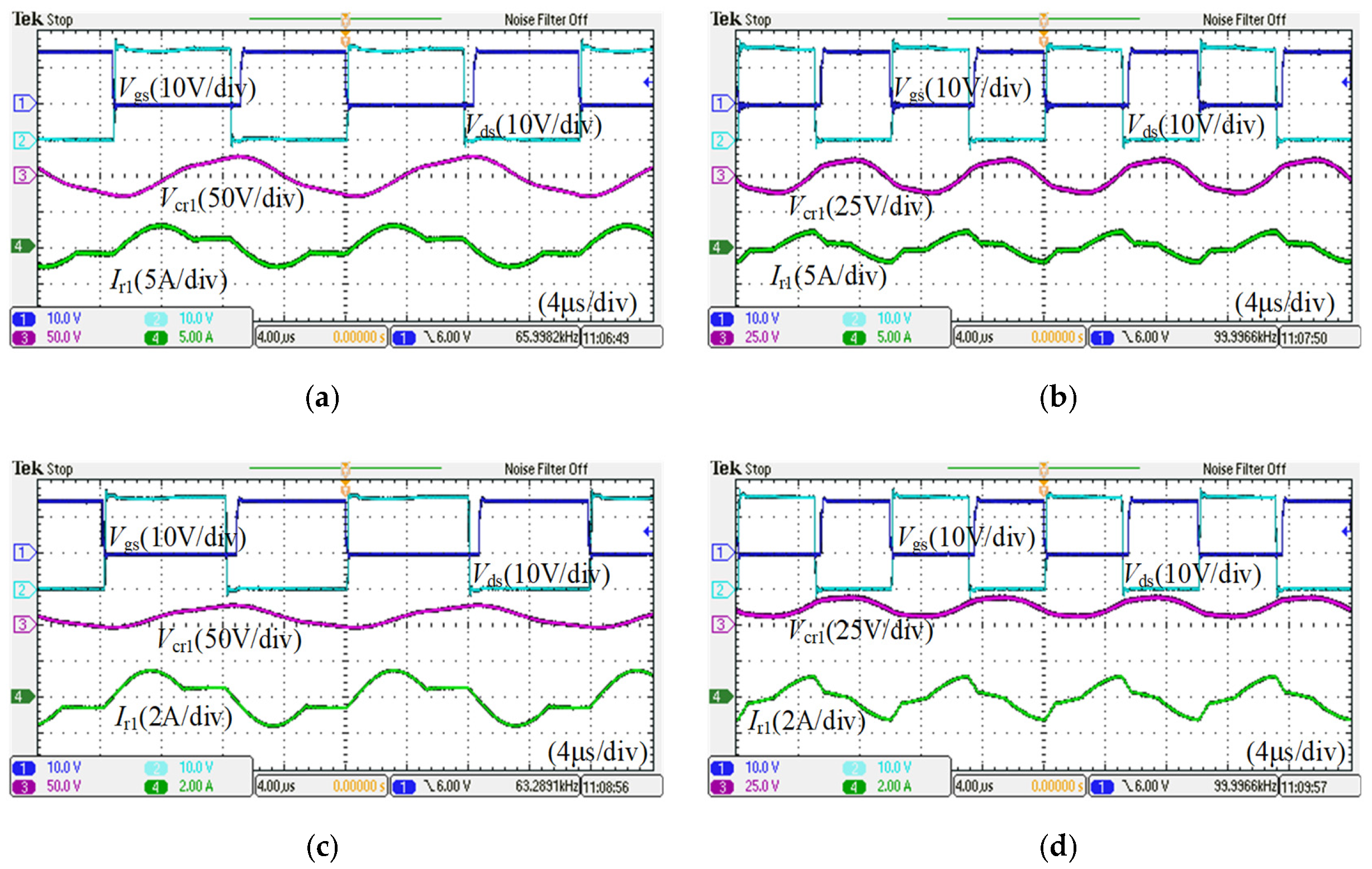
The experimental waveform shown in
Figure 16 includes the resonant current
Ir1 in tank circuit 1, the resonant capacitor voltage
Vcr1, the driving voltage
Vgs across the switching transistor Q
2 GS and the voltage
Vds across the DS. As can be seen from the figure, before
Vgs rises from 0 to 15 V,
Vds has dropped to 0, and the current value corresponding to the resonant current
Ir1 at this moment is positive, which flows through the anti-parallel diode of the power switch. Experiments show that, under the four operating modes, the power switch on the primary side can achieve zero-voltage turn-on capability.
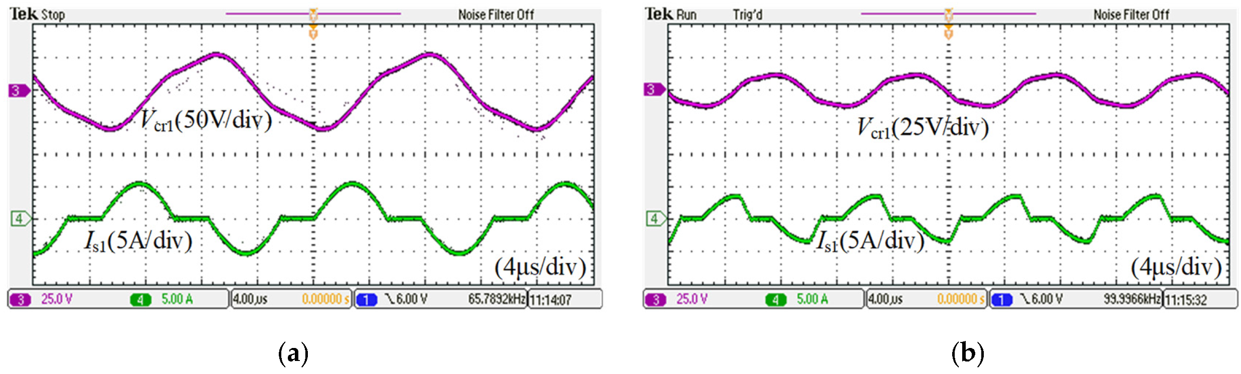
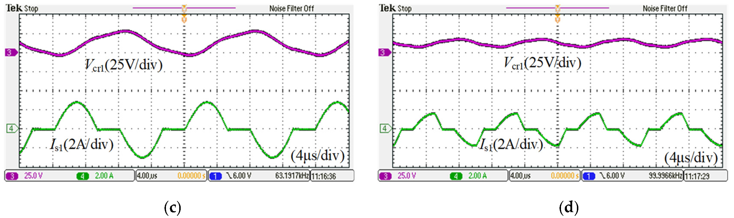
The experimental waveforms shown in
Figure 17 include the resonant capacitor voltage
Vcr1 in tank circuit 1 and the secondary current
Is1 of transformer T
1. In the frequency modulation mode, the operating frequency of the switch is greater than the resonant frequency and, within a switching cycle, the resonant current will periodically drop to the size of the excitation current, and there is no current difference between the two, so the secondary current
Is1 refracted to the transformer is also 0, as shown in
Figure 17a,c. In the phase-shift mode, although the switching frequency is fixed at the resonant frequency, because of the existence of the phase-shift angle, the resonant current will decrease in advance and the rectified current can also naturally decrease to 0, as shown in
Figure 17b,d. Experiments show that under the four operating modes, the rectifier diodes on the secondary side can achieve zero-current turn-off capability.
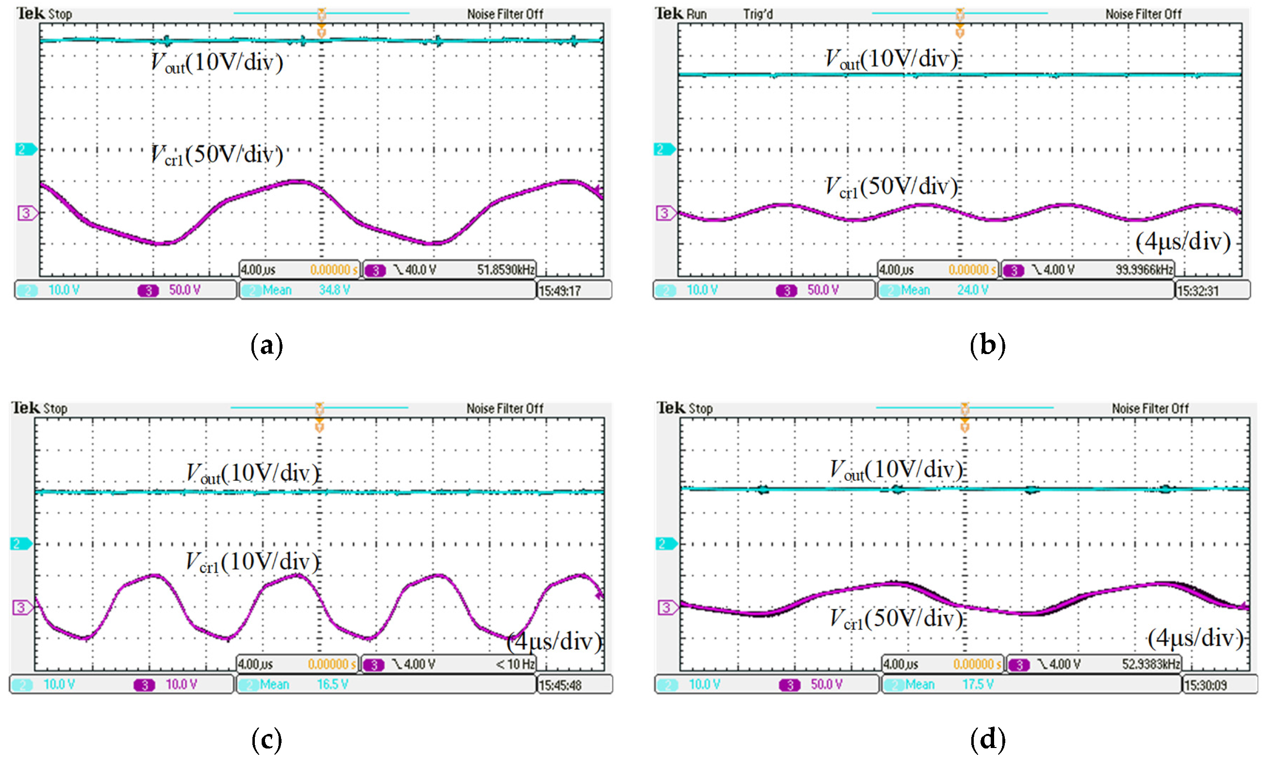
Figure 18 shows the upper and lower limits of the required output voltage in each mode when the input voltage is fixed. The experimental waveforms shown in the figure include the output voltage
Vout and the resonant capacitor voltage
Vcr1 in tank 1. In the full-bridge frequency modulation mode, the controller changes the output voltage by adjusting the frequency and the circuit belongs to the boost state. The maximum output of the circuit can reach 35 V, as shown in
Figure 18a. At this time, the resonant capacitor voltage
Vcr1 is in a sinusoidal state, the maximum amplitude is 50 V, and the switching frequency
fs = 52 kHz; when the switching frequency rises to the resonant frequency
fr, the output voltage
Vout = 24 V and the capacitor voltage
Vcr1 amplitude is 15 V, as shown in
Figure 18b. This is due to the turn-on voltage drop that exists in the circuit, which makes the circuit’s voltage gain at the resonant frequency less than ideal.
The lower limit of the output voltage in the full-bridge frequency modulation mode is also the output upper limit of the full-bridge phase-shift mode, and the phase-shift angle is 0. The controller can continue to reduce the voltage by increasing the phase-shift angle. When the output voltage
Vout = 16.5 V, the lower limit of the output voltage of the full-bridge phase-shift mode is reached, as shown in
Figure 18c. The phase-shift angle α = 0.54π and the amplitude of the resonant capacitor voltage
Vcr1 is 10 V.
The upper limit of the output voltage in the half-bridge FM mode is set to 17.5 V, as shown in
Figure 18d. The circuit switching frequency
fs = 53 kHz, the resonant capacitor voltage
Vcr1 is a sine wave with a DC offset of 12.5 V and its amplitude is 25 V; when the switching frequency reaches the resonant frequency, the output voltage
Vout = 11.8 V and the amplitude of the resonant capacitor voltage
Vcr1 is 6 V, as shown in
Figure 18e.
In the design requirements, the lower limit voltage that the half-bridge phase-shift mode needs to reach is 9 V. At this time, the phase-shift angle α = 0.52π and the amplitude of the resonant capacitor voltage
Vcr1 is 5 V, as shown in
Figure 18f. The experimental results show that the experimental prototype meets the wide output range required by the design.


