Abstract
The high penetration of new device technologies, such as Electric Vehicles (EV), and Distributed Generation (DG) in Distribution Networks (DNs) has risen new consumption requirements. In this context, it becomes crucial to implement a flexible, functional and fast responsive management of the voltage level and Reactive Power (RP) in the DN. The latest improvements in the Solid State Switches (SSS) field demonstrate they can be used as a Power Electronic (PE) converter. In particular, they have been shown to be capable of operating synchronously with transformers, making the Hybrid Distribution Transformer (HT) concept a potential and cost-effective solution to various DN control issues. In this paper, a HT-based approach consisting of augmenting the conventional Low Voltage (LV) transformer with a fractionally rated PE converter for regulating and controlling the RP in the last mile of the DN is proposed. In this way, it is expected to meet the demand of the future DN from an efficiency, controllability and volume perspective. The proposed approach is implemented using a back-to-back converter. In addition, a power transfer control topology is used to implement the proposed control of the RP injection that controls the voltage level at the Direct Current (DC) link. The proposed approach has been demonstrated in different load scenarios using the Piecewise Linear Electrical Circuit Simulation (PLECS) tool. The simulation results show that the proposed approach can compensate the loads with their need from RP instead of feeding them from the transmission grid at the primary side of the Distribution Transformer (DT). In this way, the proposed approach is able to decrease the transferred amount of RP in the transmission lines.
1. Introduction
Nowadays, the energy market is experiencing an increasing demand for Reactive Power (RP) in the last mile of networks [1]. This is mainly due to the gradual insertion of new technologies, such as Electric Vehicles (EV) [2,3,4,5,6,7] and the high penetration of Distributed Generation (DG) in the Distribution Network (DN) [8,9,10]. In this scenario, where loading type and consumption change stochastically at the end of the line, performing RP compensation in the DN becomes crucial for keeping the voltage constant [11]. In this line, new approaches should be implemented in the last mile substations towards providing more flexibility and functionality regarding voltage level [12], RP compensation, amount of demand and losses [13,14]. On the one hand, real time voltage regulation is needed, guaranteeing a specific voltage level regardless the amount of load demand. On the other hand, RP regulation is needed towards providing the load unit of the required VAr (Volt-Ampere reactive) while ensuring it is not transferred back through the transmission lines, causing losses retroactively. Moreover, in order to keep the voltage and the current in phase, the control intervention should be performed from the closest point in the network, i.e., the last mile transformer.
Traditionally, the ratio between the primary and secondary voltage in Distribution Transformers (DTs) has been fixed. In order to regulate their voltage, tap changers have largely been used. Nevertheless, on-load tap-changers are complex mechanical devices which have several issues, such as excessive conduction losses and arcing in the diverter. Although some alternatives have been introduced in the literature to solve these issues [15], the use of on-load tap changers is no longer suitable in the current scenario. This is mainly due to the fact that every transformer has a limited number of tapings in its life cycle, making voltage regulation at a real time pace not possible. In this sense, passive DTs are usually susceptible to Direct Current (DC) offset and controllability issues when employed in smart grids. In order to fulfil the current voltage control and RP regulation requirements, it is then crucial to provide DTs with more functionalities as well as a higher flexibility. The latest improvements in the field of Solid State Switches (SSS) suggest that using them as a Power Electronic (PE) converter can be a potential solution to modernise and harmonise Alternating Current (AC) and DC electrical networks [16,17]. In this line, several approaches have been proposed in the literature using full rated converters, showing they are capable of adding a huge amount of functionalities and a high controllability to DTs. Nevertheless, using full rated converters, usually located after or before the DT as a standalone device, yields high losses for switching and conduction as well as requiring high maintenance. In order to bridge this research gap, several works have been published in the literature proposing to perform VAr compensation [18,19,20], voltage regulation [21,22], or even both [23,24] using reduced ratings for the SSS. In particular, the so-called hybrid distribution transformer (HT) [25,26,27], which consists of using an embedded fractional rated converter partially attached to the windings of the DT, has been widely used [19,20,23,24,28]. In [19], the power stage design, control, and performance evaluation of a 13.2 kV/10 kVA State Switch Transformer (SST) for a power distribution system is presented. In [20], a time-domain model of a Medium Voltage (MV)/Low Voltage (LV) bidirectional SST is designed and tested under different operating conditions towards evaluating its impact on the network’s power quality. In [23], a decentralised strategy based on an adaptive droop control for promoting voltage and power balance among modules of a cascaded SST is proposed. In [24] a two stage active hybrid SST based on a multi-level converter using a Silicon Carbide (SiC) metal-oxide semiconductor field effect transistor (MOSFET) is proposed towards achieving a wide voltage and power flow control range, low filter size, and simple control sequence. Finally, in [28] a HT encompasses a three-phase DT with secondary windings arranged according to an open-end configuration and a three-phase inverter with floating DC bus. Since the HT approach proposed in [28] does not require a bidirectional converter to manage bidirectional power flows, nor a tertiary winding to supply the inverter, it allows using standard MV-LV DTs with simple modifications for voltage control at the distribution grid edge, RP management and harmonic pollution mitigation.
In this paper, a HT-based approach is proposed to provide additional functionalities to the last mile transformer. In particular, the use of the HT allows the proposed approach to smoothly regulate the voltage at a real time pace as well as to manage the RP injected in the DN. The proposed approach is based on the synchronous interaction between the SSS and the LV windings of the conventional DT. In this context, the amount of supported RP is restricted by the ratings of the fractional attached PE, whereas the SSS are controlled according to the immediate need for VAr control in the LV network [29]. In particular, due to the fact that the required percentage of voltage regulation is not usually higher than ±20% of the nominal voltage, the proposed approach only uses the 20% of the original converter ratings. According to [30], one of the main drawbacks of using converters rated for the full power rating of the grid is their high losses for switching and conduction as well as their high maintenance costs. Although losses and costs analysis are out of the scope of this paper, it is expected that since it handles only the 20% of the total power, the losses and the costs of the proposed approach would be reduced with respect to the ones associated with the use of full rated converters. Finally, it is important to highlight that the proposed approach is implemented at the last mile transformer. Locating the proposed approach as close as possible to the load has the advantage of decreasing the transferred amount of RP in the transmission lines. Consequently, the Power Factor (PF) on the other side of the network (MV network) can be improved. To the best of the authors’ knowledge, there is little to no work in the literature proposing HT implementation on the last mile transformer.
A typical configuration of a HT is shown in Figure 1. There exist different HT configurations and key aspects of designing HT towards providing the DT with additional abilities that are discussed in [31]. In general, the selection of the HT configuration depends on the desired functionality. Each configuration has its own topology, varying the configuration of the PE attachments and the connection of the new amendments with the network lines. In this paper, a back-to-back converter is attached to the last mile transformer to represent the operation of RP option. In addition, a power transfer control topology is considered by using the dq transformation technique to control the RP injection that controls the voltage level at the DC link [32]. Finally, in order to evaluate the performance of the proposed approach in different loading scenarios, simulation experiments are conducted resorting to the Piecewise Linear Electrical Circuit Simulation (PLECS) (https://www.plexim.com/plecs) tool.
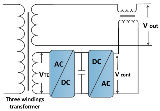
Figure 1.
The typical configuration of the HT.
2. Proposed HT Approach
The proposed approach is based on the HT concept consisting of partially attaching a fractional rated PE converter to the LV transformer’s windings [25]. The fractionally in the ratings of the transformer is mainly aimed at providing the whole RP compensation system with the following characteristics:
- High reliability, but low cost when compared to full rated converts.
- Reducing switching losses due to operating within lower switches’ ratings.
- Exploiting the latent advantages of one of the most reliable devices in the network, i.e., the transformer.
- The system partially tastes the flexibility of the PE and its functionalities that could be bypassed in case of PE failure.
2.1. HT Design
If only a ±10% voltage limit for regulation is considered by the regulator, the attached SSS of the converter can be designed at fractional ratings (around 20–30%) of the total windings of the LV transformer. These ratings allow control of the voltage regulation interval and cut from the total power (S) part of the RP by making the angle between voltage and current around 20% [26]. In this paper, different control configurations are proposed towards achieving the following characteristics:
- Voltage regulation of up to ±30% of the nominal value.
- RP control of up to ±30% of the nominal value.
In addition, if the total rating of the PE part is not exceeded, a combination of voltage regulation and RP control can be achieved. Finally, it is important to highlight that, in the proposed approach, the attached PE converter can be cancelled and protected by being bypassed in case of a failure within the system.
There exist different conceptual schematics for the design of the HT. Each one of them have different functionalities in serving different demands in the last mile of the network according to the VAr control scenario. In this paper, the PE consists of a back-to-back converter so that the operation of RP option is represented. The chosen converter has several advantages:
- It performs fast control for power flow.
- If the power at the DC link from the rectifier and inverter sides is balanced, the variations in the DC voltage at the DC link can be avoided [33]. In this way, the current level at the DC link is not distorted.
- A DC output can be supplied in case of further modifications.
In the proposed approach, the back-to-back converter is set up to control three unbalanced phases separately. Each phase supplies three feeders in the last mile of the network, making a total of nine lines. The three phases differ in length and the number of connected loads, having different voltages drops and different demands. In this context, a separate voltage regulation and VAr compensation is needed for each phase [34]. This can be done either by using three single converters, or by using a three-phase converter. Figure 2 shows the proposed approach in this paper, where the HT is introduced as a normal transformer that is partially attached to an AC/AC converter with a DC link and a series transformer. The AC/AC converter in Figure 2 has two main functionalities. On the one hand, it keeps the voltage constant at the regulated line. On the other hand, it injects/absorbs a specific amount of RP, which is restricted by the fractional ratings of the SSS of the transformer. Finally, it is important to highlight that, as discussed in Section 1, flexibility is a key aspect for any RP compensation solution. In this line, the proposed HT-based approach shown in Figure 2 has the advantage of being flexible, allowing the injected/absorbed amount of RP to be increased by including more reliable PE switches.
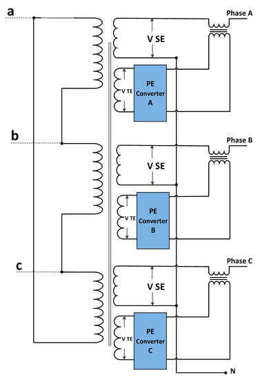
Figure 2.
The proposed HT-based approach, which is a conventional transformer that is attached partially to an AC/AC converter with a DC link and series transformer.
2.2. HT Topology
Different HT configurations can be used depending on the specific issue that is desired to be addressed in the last mile of the network, viz., voltage regulation, voltage stability, RP flow or VAr compensation. Each configuration has its own topology and differs in the PE attachments and the connection of the new amendments with the network lines. Table 1 shows different schemes for different HT configurations and describes their main functionalities. As discussed in Section 2.1, in this paper the PE consists of a back-to-back converter, which corresponds to the configurations of Figure 3c,d shown in Table 1. In particular, the selected converter has the following advantages:

Table 1.
Different schemes and their functionalities.
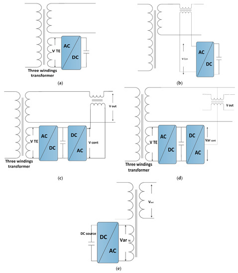
Figure 3.
(a) Conceptual 1, a converter attached separately to tertiary winding; (b) Conceptual 2 with a converter supporting the secondary side; (c) Conceptual 3, back-to-back converter supporting the secondary sides in series mode; (d) Conceptual 4, back-to-back converter supporting the secondary sides in parallel mode; (e) Conceptual 5, a converter attached to the primary side.
- It provides a fast control for the power flow.
- It avoids variations in the DC voltage at the DC link.
- It keeps the current level undistorted when the power at the DC link from the rectifier and inverter sides is balanced [33].
2.3. HT Implementation
Figure 4 shows in detail the fractional rated back-to-back converter used in the proposed approach presented in Figure 2 together with its control approach.
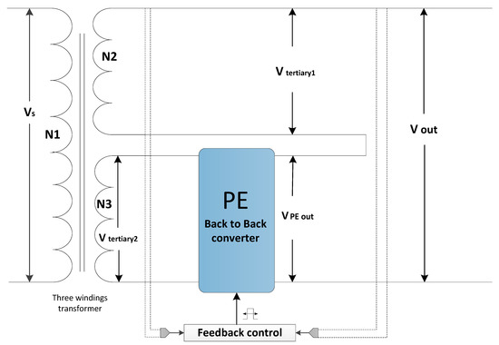
Figure 4.
Detail of the proposed HT approach, where the proposed control circuit is introduced.
In Figure 4, the transformer ratios are as follows [29]:
where Vs is the primary voltage, VPE out is the output voltage of the converter, D is the duty cycle of the Pulse-Width Modulation (PWM) signal and N1, N2, and N3 are the turns ratio of the transformer. It is important to highlight that, in the proposed approach shown in Figure 4, N2 is smaller than N1, and N3 is smaller than N2. Then, Vout can be expressed as in Equations (4) and (5):
3. Proposed HT Control Approach
For the proposed approach based on the back-to-back converter shown in Figure 5, the voltage and the RP supply should be controlled. In this paper, a dq transformation technique is proposed to control the voltage at the DC link terminals [32]. In this way, the overall controller adds or decreases the voltage to/from the total output voltage in order to control the whole output voltage of the transformer [37]. On the other hand, a vector control is proposed to control the supply of RP since it is one of the most popular methods used for Voltage Source Converters (VSC) [37]. Figure 5 shows the proposed PE converter design structure of the VSC in the DC side. As can be seen from Figure 5, the rectifier side controls the voltage at the DC voltage and the RP injection, while the inverter side controls the active power. In addition, the RP can also be controlled in both converters separately without affecting the DC voltage. In this way, the chosen back-to-back converter has the advantage of allowing controlling the RP, the active power, the AC voltage and the DC voltage [38]. The different strategies proposed in this paper to control them are presented and discussed in the following subsections.
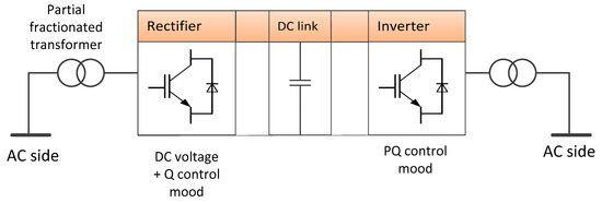
Figure 5.
The overall PE design structure of the Voltage Source Converter (VSC) in the DC side.
3.1. Voltage Control Approach
For the proposed approach shown in Figure 6, the voltage control strategy is applied in case of over-voltage or under-voltage incidents at the output of the transformer. In particular, the voltage control is performed as a balance between the output of the secondary windings and the AC-AC converter, increasing or decreasing the voltage in a range of 10–20% to/from the total output voltage, as introduced in Section 2.2, in order to control the whole output voltage of the transformer. In the proposed approach, the transformer supports a part of the supplied voltage and the PE converter controls the other part of the voltage, i.e., the voltage variations. In this line, if a voltage decrease occurs in the distribution line, the converter duty ratio (D) increases, whereas when a voltage increase occurs, D decreases [15]. Figure 6 shows the vector diagram of the proposed voltage control.
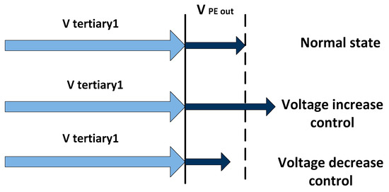
Figure 6.
A vector diagram of the proposed voltage control.
As introduced above, the DC link of the back-to-back converter is controlled by using a dq transformation [32]. In addition, the AC side of the converter (Vout) is controlled using a Resonant Controller (RC). Figure 7 shows the schematic diagram of the overall control of the output voltage. As can be seen from Figure 7, the output voltage of the converter Vcon is controlled to add or decrease the voltage to the overall output voltage of the phase (VA output, VB output, and VC output). In addition, in order to obtain a sinusoidal wave output, an LC filter is included [21].
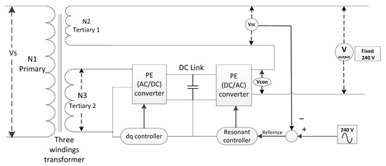
Figure 7.
A schematic diagram of the overall control of the output voltage.
Figure 8 shows the control logic used to perform the control of the overall output voltage for the proposed HT approach.
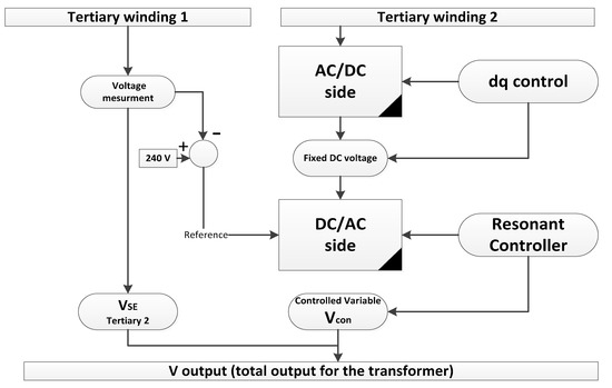
Figure 8.
The proposed control logic. A schematic diagram of the overall control of the output voltage.
3.2. Reactive and Active Power Control
The power angle control is a widely known principle used to control active and reactive power. Let X and R be the reactance and resistance of the transmission element. In cases where the X:R ratio is very high, the active and reactive power can be computed by Equations (6) and (7), respectively:
where and are the voltage values in the electrical nodes 1 and 2, respectively, is the difference of voltage angles (load angle) = δ1 − δ2. and is the line reactance. In the HT-based approach proposed in this paper, the transformer is considered as the transmission element. In this sense, the X:R ratio of the transmission element is very high, enabling the use of Equations (6) and (7) as the fundamentals of the power angle control [39]. According to them, the power can be controlled through controlling the power angle between two electrical points. Nevertheless, the power angle control principle is rarely used in the practice due to its numerous disadvantages, such as the limitations in controlling the current and bandwidth in converters [40], which can lead to serious problems regarding protection [39]. In this paper, the reactive and active power are then controlled by resorting to a vector control. In order to do so, the active and reactive power are first transformed into the dq domain as shown in Equations (8) and (9):
where and are the voltages and currents in the dq coordinates. The active and reactive power in Equations (8) and (9) are then controlled by the proposed Proportional Integral (PI) controller shown in Figure 9. In Figure 9, Qref and Pref are the desired values of the reactive and active power, respectively, whereas Q and P are the measured values of the reactive and active power, respectively. Finally, iqmax is the maximum value for Iq.
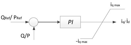
Figure 9.
The dq frame reactive and active power controller.
3.3. DC Link Control Using Power Control Principle
As introduced in Section 3, the back-to-back converter is used in this paper since it has several advantages. In particular, it avoids the variations in the DC voltage at the DC link and keeps its current undistorted whenever the power at the DC link from the rectifier and inverter sides is balanced. The size of the DC link plays an important role in the balance of the power transfer between the converter and the grid. In general, minimising the capacitor size allows for a reduction in the total cost and volume of the design. Nevertheless, installing small size DC links or capacitors increases the possibility of current distortion and voltage variations at the inverter output. Furthermore, small capacity contributes to DC ripples whenever the AC voltage source is affected with harmonics or unbalanced situations [41]. In this context, it is crucial to reach a trade-off between the total cost of the design and the ripple and voltage fluctuation tolerance. Some control approaches have been proposed in the literature to mitigate the undesired effects of small capacity. For instance, in [42] film capacitors are used for energy storage at the DC link. Nevertheless, the available approaches in the literature do not usually take into account the power balance between the inverter and the rectifier. In this paper, the DC link voltage is controlled by taking into account the power balance between both converters. This leads to several control advantages. On the one hand, since the operation of the rectifier depends on the operation of the inverter status, considering the power flow dynamics between them contributes to fasten the proposed control. On the other hand, and more importantly, taking the power balancing into account allows the rectifier to control the active or reactive current. In this way, the inverter is allowed to be fed with the exact amount it needs from current. Consequently, voltage fluctuations are avoided by controlling the amount of current that flows through the DC link. Finally, for the proposed approach, the stored energy () and the power in the capacitor () are represented as shown in Equations (10) and (11). The relation between them is shown in Equation (12):
3.4. Inverter and Rectifier Power Dynamics
As discussed in Section 3.2, taking into account the power balance between the inverter and the rectifier leads to several advantages; in particular, allowing us to avoid voltage fluctuations by controlling the amount of current that flows through the DC link is the most important advantage. In order to better understand the inverter and rectifier power dynamics, they are introduced in the following subsections, respectively.
3.4.1. Inverter Dynamics
Figure 10 shows the schematic diagram of the inverter connected with the grid. According to Figure 10, the output voltage can be written as shown in Equation (13) [40]:
where variables in [] are vector variables. In particular, [] is the grid voltage, [] and [] are the converter input voltage and current, respectively, and and are the inductance and resistance between the converter and grid, respectively. After dq transformation, Equation (13) can be written as in Equations (14) and (15) [40]:
where ω is the angular frequency. The line currents derivation is shown in Equations (16) and (17):
Figure 10.
A schematic diagram of the inverter connected with the grid.
The inverter voltage derivation is shown Equations (18) and (19) [40,43]:
where and are the PI control coefficients, and are the errors represented as () and in the dq transformation frame. Finally, and are the reference feed in the current control loop. Then, the inverter power that is taken from the DC link is given by Equation (20):
By substituting the values of Equations (16) to (19) in the derivation of Equation (20), and simplifying them, the inverter power dynamic is given by Equation (21):
where is the inverter power dynamic variable used by the inverter to update the rectifier with the current status of the inverter. This enhances the current control at the DC link between the rectifier and inverter.
3.4.2. Inverter Dynamics
As discussed in Section 3.2, in the proposed approach, the rectifier operates according to the controlled status of the inverter. In this context, the rectifier is governed, according to the inverter power dynamics, by the power transfer dynamics in Equations (22)–(24):
where is the capacitor voltage, and / are the dq axis of the rectifier terminal voltages and currents, respectively, and ω is the source voltage angular frequency. Suppose and bring into line the q frame control, then the power from the rectifier to the DC link is obtained as shown in Equation (25):
In case of supposing Eq = 0:
3.5. Transfer Function for Power Control
Since the inverter side is connected to the LV side of the grid, it is in charge of the synchronisation of the system. The rectifier, on its part, acts as the source gate for the inverter. Therefore, the rectifier follows the power dynamics of the inverter. From Equation (21), the transfer function of the inverter can be deduced as follows:
According to Equations (26) and (27), the transfer function of the rectifier is given by:
Then:
where is the control coefficient. From Equations (12), (29) and (30), the control diagram for the DC link is implemented as in Figure 11.
Figure 11.
The control loop for the DC link.
The feedback for the closed loop in Figure 10 is the error between the power and its reference as shown in Equation (32):
Finally, the whole control system proposed in this paper for the converter is shown in Figure 12. As can be seen from Figure 12, the main control topology depends on the power transfer strategy between both converters. In particular, the control system depends on the power dynamics between the inverter, which is connected to the LV side, and the rectifier, which is connected to the transformer. The control strategy shown in Figure 12 is implemented as follows. The control divides the power into two terms, namely d, corresponding to the active power, and q, corresponding to the RP. Voltages and currents are described as vectors in the stationary αβ and transformed to dq coordinates to be controlled via two loops. The inner loop controls the current, whereas the outer loop controls the DC voltage. The controlled coordinates are then transformed to feed the PWM generator towards controlling the DC output of the converter [44]. Finally, an equivalent Laplace transformation for the circuits’ material is performed in order to determine the parameters of the PI controller. Here, it is important to highlight that, by applying the proposed control, the fluctuation in the DC link is minimised, enabling a fast and stable control for the AC side of the converter.
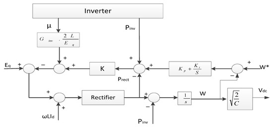
Figure 12.
A schematic diagram of the power control system.
4. Results and Discussion
In order to evaluate the capability of the proposed approach to control the output voltage and compensate the load with its need from RP, different simulation experiments are conducted resorting to the PLECS simulation tool. In particular, the AC side of the converter is simulated operating under different loading scenarios in order to assess the robustness of the proposed approach. In Section 4.1, the control voltage results are presented and discussed, whereas the results for the RP control are presented and discussed in Section 4.2. The parameter values used to configure the corresponding circuits of the proposed approach and perform the simulations with the PLECS tool are shown in Table 2. As shown in Table 2, the switching frequency ƒs is equal 5 KHz. Consequently, the converter time delay average is = = s. Finally, the capacitance of the DC link is: = 312.5 µF, where F stands for faraday.
Table 2.
The parameter values for circuit configuration in the proposed approach *.
4.1. Voltage Control Results
As introduced in Section 3.1, the DC link of the back-to-back converter is controlled by using a dq transformation [32], its main aim being to maintain the DC voltage fixed at the terminal of the linked capacitor in order to provide the AC part of the converter with a stable source of power. In this way, the DC output is allowed to respond to the reference of the controller and step up/down to the required value, as shown in Figure 13.
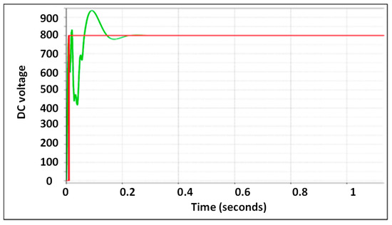
Figure 13.
The voltage control response for the DC link.
In addition, the AC side of the converter is controlled using a RC. An advantage of using such controller is that it can also be used to eliminate specific harmonics at specific frequencies by applying their frequencies in parallel implementations for the term frequency (TF) functions. The harmonic elimination is carried out as in Equation (33), being further illustrated in Figure 14. In Equation (33) and Figure 14, the control operates at the frequencies of the harmonics that need to be eliminated [45], where the fundamental frequency is .
where KC is the control gain for the fundamental frequency, and Kca, Kcb and Kcm are the control gains for other chosen frequencies, such as 150, 250, and 350 Hz, respectively, for the purpose of harmonic distortion.
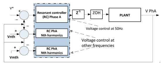
Figure 14.
The Resonant Controller (RC) for voltage control at 50 Hz and different harmonics elimination.
In the proposed approach, the Proportional Resonant (PR) controller and the high order controller are tuned in such a way that a high stability margin is achieved. This is can be seen in the root locus (Figure 15a) and the Bode plot diagram (Figure 15b) in Figure 15 for a damping factor of 0.7, whereas the step response for the control system is shown in Figure 16.
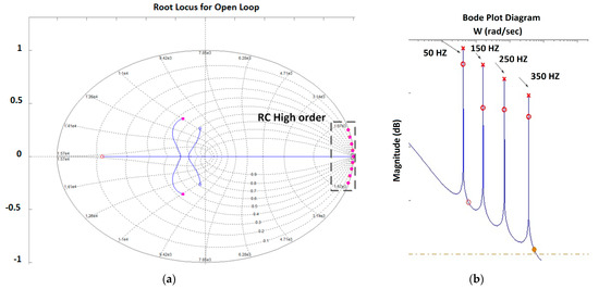
Figure 15.
The root locus (a) and Bode plot diagram (b) for the RC control.
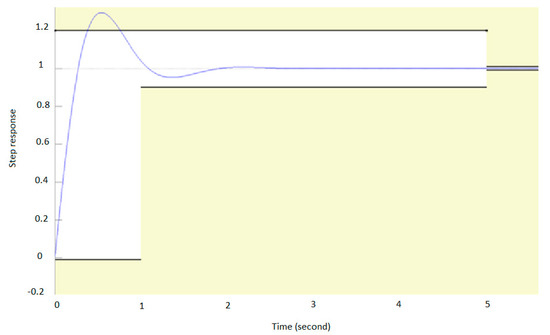
Figure 16.
The step response of the control system.
Finally, in order to evaluate its robustness, the proposed voltage control approach is applied within different operating scenarios. In this line, different loading conditions including voltage variations, such as sags and short transient time, are considered. In particular, voltage fluctuations, such as sag and swell, are simulated by considering heavy loads and light loads applied before the main load in order to cause a disturbance scenario decreasing or increasing the voltage. In the first simulated scenario, the output voltage is fixed at the secondary side of the HT at 246 V (Root Mean Squared (RMS) value) and a voltage swell is applied on the circuit. Figure 17 shows the control system response to the applied voltage swell. As can be seen from Figure 17, the overall control forces the voltage to settle down to its reference value after 1.5 s.
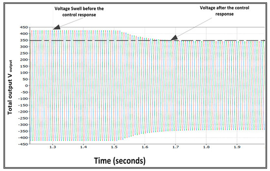
Figure 17.
The overall control response to a voltage swell.
In addition, the proposed voltage control approach allows regulating the voltage over frequent transient voltage fluctuations (second by second). This is illustrated in Figure 18, where the response of the proposed control system to a voltage sag and voltage swell applied on the output voltage during 4 s, is shown. As can be seen from Figure 18, the reference of the total output voltage control is fixed and controlled at the nominal voltage level. In this way, the voltage regulation interval is decreased from ±10% to almost ±0%.
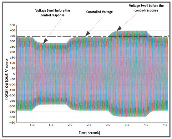
Figure 18.
Voltage fluctuation regulation.
The results shown in Figure 17 and Figure 18 show that the proposed control voltage approach is capable of controlling the voltage output during single and frequent time variations. In particular, the control of switches provides a stable DC link as a first level of control in order to isolate the variations of the input from the output. This ensures a stable operation for the control at the AC side, which is the final voltage output. In addition, as can be seen from Figure 18, the proposed control approach has a response time of nearly one second. In this regard, the proposed approach outperforms similar voltage regulation approaches recently proposed in the literature. For instance, in [46] a partially rated PE assisted On-Load Tap Changing (OLTC) autotransformer is presented for grid voltage regulation. Although the results obtained in [46] show their control voltage approach is capable of handling frequent voltage fluctuations, the time response is higher than the one obtained in this paper. Finally, the obtained results in this paper are promising since they improve the system operation under sensitive voltage load conditions which require a steady and accurate voltage level with a quick time response, such as medical equipment applications. On the one hand, over-voltage in such applications can damage the electronic devices, reducing their operational life. On the other hand, decreasing the voltage in such applications can result in disabling the operation of these sensitive devices.
4.2. RP Compensation Results
The proposed control for the RP compensation is tested according to the scheme shown in Figure 19. As can be seen from Figure 19, the HT is controlled to support the load with its partial need from RP, instead of taking it from the transmission grid. In this way, the q component that is transferred from the transmission line is zero, being produced only by the HT. A classic dq transformation technique is used for the proposed fractional converter as shown in Figure 20. Using the dq transformation scheme shown in Figure 20 allows transference of the three-phased input into two DC items in such a way that they can be controlled over the DC link at the link between both sides of the back-to-back converter. From Figure 20 it can be seen that, since the dq transformation is used, the q components represent the reactive power or the current part.
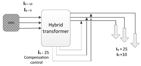
Figure 19.
The control diagram for the proposed RP compensation control.
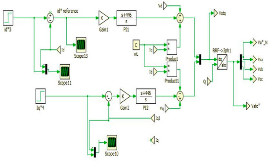
Figure 20.
The dq transformation technique for the fractional converter.
The results obtained for the different considered loading scenarios regarding the injected RP, the transferred VAr through the transmission grid and the loaded RP after the secondary side of the transformer are presented and discussed in the following subsections.
4.2.1. Loading Scenario (L1)
In this scenario, the RP that is transferred through the transmission line before the 11/0.43 KV transformer, is zero. In this context, the load takes its RP need from the HT. Figure 21a–c shows the Id and Iq for the injected RP, the transferred current in the transmission lines, and the distributed current for this loading scenario, respectively. As can be seen from Figure 21a–c, the proposed approach is capable of efficiently regulating the transfer voltage in the described loading scenario in much less than one second. In this way, the proposed approach achieves a good regulating performance significantly faster than the conventional voltage regulation method based on tap-changers [47].
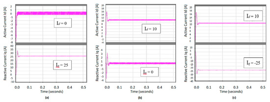
Figure 21.
(a) The dq components of the injected RP for the loading scenario (L1); (b) the dq components of the transferred current in the transmission lines for L1; (c) the dq components of the distributed current for L1.
4.2.2. Loading Scenario (L2)
In this scenario, the RP demand is increased. The load takes most of its RP need from the HT and the rest is transferred through the grid. Figure 22a–c shows the Id and Iq for the injected RP, the transferred current in the transmission lines, and the distributed current for this loading scenario, respectively. As can be seen from these figures, the transferred RP (before the HT) is decreased. In this case, the ratings of the PE in the HT could be increased towards fulfilling the increasing demand of RP for the connected loads, confirming that the PE ratings and the HT capability of supplying RP depend mainly on the nature of the loads. Nevertheless, increasing the PE ratings would lead to an increase in the cost and the losses. In addition, as in the case of the previous loading scenario (L1), in this loading scenario (L2) the proposed approach also regulates the voltage in much less than one second, outperforming the traditionally used voltage regulation method [47].
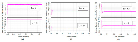
Figure 22.
(a) the dq components of the injected RP for the loading scenario (L2); (b) the dq components of the distributed current for L2; (c) the dq components of the transferred current in the transmission lines for L2.
Finally, it is important to highlight that the DC link/source can be further improved towards providing a DC output source for a DC line in an enhanced form of the control. In this way, it could operate synchronously between providing stability for the AC side and feeding a DC line. This approach would be similar to the Uninterrupted Power System (UPS) approach presented in [48].
5. Conclusions
An increasing RP demand is expected in a near future due to the high penetration of DG in the DN and the increasing use of new technologies such as EVs. The main focus of this paper was to validate the concept and usability of HT in providing real time voltage control in the last mile of the network. Although locating the HT as close as possible to the load has the advantage of decreasing the transferred amount of RP in the transmission lines, improving the PF on the other side of the MV network, there is a lack of works in the literature addressing last mile transformers’ issues. It is the authors’ intention that the HT approach proposed in this paper and its promising results can set the basis for the future choice for LV substation features by initialising a reasonable percentage of SSS working synchronously with the last mile transformer.
The proposed HT approach was based on the use of a back-to-back converter to represent the PE, allowing a fast control for power flow, avoiding the variations in the DC voltage at the DC link, and keeping the current undistorted whenever the power at the DC link from the rectifier and inverter sides is balanced. In this way, the proposed DC control approach took into account the power balancing between the inverter and the rectifier, avoiding voltage fluctuations by controlling the amount of current that flows through the DC link. This constitutes a key aspect of the proposed approach, since most of the approaches in the literature do not take this power balancing into account, leading to undesired current distortion and voltage variations at the inverter output.
The simulation results obtained for different real time voltage operating scenarios, including voltage swells, sags and short transient time, showed the capability of the proposed HT approach for controlling the voltage when single and frequent time voltage variations occur. In this sense, the proposed approach has been demonstrated to be well suited for applications operating under sensitive voltage load conditions which require a steady and accurate voltage level as well as a quick time response, such as medical equipment applications. In addition, the simulations have also shown that the proposed approach can compensate different loads with their need from RP instead of feeding them from the transmission grid at the primary side of the DT. In this way, the transferred amount of RP in the transmission lines is decreased.
Author Contributions
Conceptualization, M.R.; Methodology, M.R.; Supervision, M.D.; Writing–original draft, M.R.; Writing–review & editing, M.D., G.T. and I.P. All authors have read and agreed to the published version of the manuscript.
Funding
This research received no external funding.
Institutional Review Board Statement
Not applicable.
Informed Consent Statement
Not applicable.
Data Availability Statement
No new data were created or analysed in this study. Data sharing is not applicable to this article.
Conflicts of Interest
The authors declare no conflict of interest.
References
- Muttaqi, K.M.; Islam, M.R.; Sutanto, D. Future Power Distribution Grids: Integration of Renewable Energy, Energy Storage, Electric Vehicles, Superconductor, and Magnetic Bus. IEEE Trans. Appl. Supercond. 2019, 29, 1–5. [Google Scholar] [CrossRef]
- Qian, K.; Zhou, C.; Allan, M.; Yuan, Y. Modeling of load demand due to EV battery charging in distribution systems. IEEE Trans. Power Syst. 2011, 26, 802–810. [Google Scholar] [CrossRef]
- Green, R.C.; Wang, L.; Alam, M. The impact of plug-in hybrid electric vehicles on distribution networks: A review and outlook. Renew. Sustain. Energy Rev. 2011, 15, 544–553. [Google Scholar] [CrossRef]
- Boglou, V.; Karavas, C.; Arvanitis, K.; Karlis, A. A Fuzzy Energy Management Strategy for the Coordination of Electric Vehicle Charging in Low Voltage Distribution Grids. Energies 2020, 13, 3709. [Google Scholar] [CrossRef]
- Coignard, J.; MacDougall, P.; Stadtmueller, F.; Vrettos, E. Will Electric Vehicles Drive Distribution Grid Upgrades?: The Case of California. IEEE Electrif. Mag. 2019, 7, 46–56. [Google Scholar] [CrossRef]
- Anastasiadis, A.G.; Kondylis, G.P.; Polyzakis, A.; Vokas, G. Effects of Increased Electric Vehicles into a Distribution Network. Energy Procedia 2019, 157, 586–593. [Google Scholar] [CrossRef]
- Spitzer, M.; Schlund, J.; Apostolaki-Iosifidou, E.; Pruckner, M. Optimized Integration of Electric Vehicles in Low Voltage Distribution Grids. Energies 2019, 12, 4059. [Google Scholar] [CrossRef]
- Caramanis, M.; Ntakou, E.; Hogan, W.W.; Chakrabortty, A.; Schoene, J. Co-Optimization of Power and Reserves in Dynamic T&D Power Markets With Nondispatchable Renewable Generation and Distributed Energy Resources. Proc. IEEE 2016, 104, 807–836. [Google Scholar] [CrossRef]
- Sarimuthu, C.R.; Ramachandaramurthy, V.K.; Mokhlis, H.; Agileswari, K.R. Impact of distributed generation on voltage profile in radial feeder. Indones. J. Electr. Eng. Comput. Sci. 2017, 6, 583–590. [Google Scholar] [CrossRef]
- Chamandoust, H.; Derakhshan, G.; Hakimi, S.M.; Bahramara, S. Tri-objective scheduling of residential smart electrical distribution grids with optimal joint of responsive loads with renewable energy sources. J. Energy Storage 2020, 27, 101112. [Google Scholar] [CrossRef]
- Reshikeshan, S.S.M.; Matthiesen, S.L.; Illindala, M.S. Autonomous Voltage Regulation by Distributed PV Inverters with Minimal Inter-Node Interference. In Proceedings of the 2020 IEEE/IAS 56th Industrial and Commercial Power Systems Technical Conference (I&CPS), Las Vegas, NV, USA, 29 June–28 July 2020; pp. 1–8. [Google Scholar]
- Zhiqun, W.; Shouzhen, Z.; Shuangxi, Z.; Renle, H.; Liangui, W. Impacts of distributed generation on distribution system voltage profile. Autom. Electr. Power Syst. 2004, 16, 014. [Google Scholar]
- Kaloudas, C.G.; Ochoa, L.F.; Marshall, B.; Majithia, S.; Fletcher, I. Assessing the future trends of reactive power demand of distribution networks. IEEE Trans.Power Syst. 2017, 32, 4278–4288. [Google Scholar] [CrossRef]
- Swami, S.; Wagle, S. Addressing Last Mile Electricity Distribution Problems: Study of Performance of SHGs in Odisha. In Proceedings of the 7th International Conference on Advances in Energy Research; Springer: Singapore; pp. 515–523.
- Gao, D.; Lu, Q.; Luo, J. A New Scheme for on-Load Tap-Changer of Transformers. In Proceedings of the PowerCon 2002—2002 International Conference on Power System Technology, Proceedings, Kunming, China, 13–17 October 2002; Volume 2, pp. 1016–1020. [Google Scholar]
- Shamshuddin, M.A.; Rojas, F.; Cardenas, R.; Pereda, J.; Diaz, M.; Kennel, R. Solid State Transformers: Concepts, Classification, and Control. Energies 2020, 13, 2319. [Google Scholar] [CrossRef]
- Farnesi, S.; Marchesoni, M.; Passalacqua, M.; Vaccaro, L. Solid-State Transformers in Locomotives Fed through AC Lines: A Review and Future Developments. Energies 2019, 12, 4711. [Google Scholar] [CrossRef]
- Radi, M.A.; Darwish, M. Var Control Considerations for the Design of Hybrid Distribution Transformers. In Proceedings of the 11th IET International Conference on AC and DC Power Transmission, Birmingham, UK, 10–12 February 2015; pp. 1–9. [Google Scholar]
- Lim, J.-W.; Cho, Y.; Lee, H.-S.; Cho, K.-Y. Design and control of a 13.2 kV/10 kVA single-phase solid-state-transformer with 1.7 kV SiC devices. Energies 2018, 11, 201. [Google Scholar] [CrossRef]
- Martin-Arnedo, J.; González-Molina, F.; Martinez-Velasco, J.; Adabi, E. EMTP model of a bidirectional cascaded multilevel solid state transformer for distribution system studies. Energies 2017, 10, 521. [Google Scholar] [CrossRef]
- Radi, M.A.; Darwish, M.; Alqarni, M. Voltage Regulation Considerations for the Design of Hybrid Distribution Transformers. In Proceedings of the 2014 49th International Universities Power Engineering Conference (UPEC), Cluj-Napoca, Romania, 2–5 September 2014; pp. 1–6. [Google Scholar]
- Szcześniak, P.; Tadra, G.; Kaniewski, J.; Fedyczak, Z. Model predictive control algorithm of AC voltage stabilizer based on hybrid transformer with a matrix converter. Electr. Power Syst. Res. 2019, 170, 222–228. [Google Scholar] [CrossRef]
- Rodrigues, W.A.; De Oliveira, T.; Morais, L.M.F.; Rosa, A. Voltage and Power Balance Strategy without Communication for a Modular Solid State Transformer Based on Adaptive Droop Control. Energies 2018, 11, 1802. [Google Scholar] [CrossRef]
- Yun, C.; Cho, Y. Active Hybrid Solid State Transformer Based on Multi-Level Converter Using SiC MOSFET. Energies 2019, 12, 66. [Google Scholar] [CrossRef]
- Bala, S.; Das, D.; Aeloiza, E.; Maitra, A.; Rajagopalan, S. Hybrid Distribution Transformer: Concept Development and Field Demonstration. In Proceedings of the 2012 IEEE Energy Conversion Congress and Exposition (ECCE), Raleigh, NC, USA, 15–20 September 2012; pp. 4061–4068. [Google Scholar]
- Sastry, J.; Bala, S. Considerations for the Design of Power Electronic Modules for Hybrid Distribution Transformers. In Proceedings of the 2013 IEEE Energy Conversion Congress and Exposition, Denver, CO, USA, 15–19 September 2013; pp. 1422–1428. [Google Scholar]
- Zhao, J.; Zirka, S.E.; Moroz, Y.I.; Arturi, C.M. Structure and properties of the hybrid and topological transformer models. Int. J. Electr. Power Energy Syst. 2020, 118, 105785. [Google Scholar] [CrossRef]
- Foti, S.; Caro, S.D.; Testa, A.; Tornello, L.D.; Scelba, G.; Cacciato, M. An Open-End Winding Hybrid Transformer. In Proceedings of the 2020 International Symposium on Power Electronics, Electrical Drives, Automation and Motion (SPEEDAM), Sorrento, Italy, 24–26 June 2020; pp. 173–177. [Google Scholar]
- Yamaguchi, K.; Lee, K.; Kurokawa, K. Study on Voltage Regulation Method in the Power Distribution System. In Proceedings of the 2007 7th Internatonal Conference on Power Electronics, Daegu, Korea, 22–26 October 2007; pp. 488–492. [Google Scholar]
- Purgat, P.; Prakoso, R.A.; Mackay, L.; Qin, Z.; Ramirez-Elizondo, L.; Bauer, P. A Partially Rated DC-DC Converter for Power Flow Control in Meshed LVDC Distribution Grids. In Proceedings of the 2018 IEEE Applied Power Electronics Conference and Exposition (APEC), San Antonio, TX, USA, 4–8 March 2018; pp. 1591–1596. [Google Scholar]
- Radi, M.A.M. Power Electronics Considerations for Voltage Regulation and VAR Control Approaches in LV Distribution Networks–Hybrid Power Electronic Modules By. Ph.D. Thesis, Brunel University London, Uxbridge, UK, 2016. [Google Scholar]
- Silva, S.M.; Lopes, B.M.; Filho, B.J.C.; Campana, R.P.; Bosventura, W.C. Performance Evaluation of PLL Algorithms for Single-phase Grid-Connected Systems. In Proceedings of the Conference Record of the 2004 IEEE Industry Applications Conference, 2004. 39th IAS Annual Meeting, Seattle, WA, USA, 3–7 October 2004; Volume 4, pp. 2259–2263. [Google Scholar]
- Hur, N.; Jung, J.; Nam, K. A fast dynamic DC-link power-balancing scheme for a PWM converter-inverter system. IEEE Trans. Ind. Electron. 2001, 48, 794–803. [Google Scholar]
- Felber, L.; Arango, H.; Bonatto, B.; Gouvea, M. Voltage Regulation in Electric Energy Distribution Substations. In Proceedings of the 2010 IEEE/PES Transmission and Distribution Conference and Exposition: Latin America (T&D-LA), Sao Paulo, Brazil, 8–10 November 2010; pp. 846–852. [Google Scholar]
- Sen, K.K. SSSC-static synchronous series compensator: Theory, modeling, and application. IEEE Trans. Power Deliv. 1998, 13, 241–246. [Google Scholar] [CrossRef]
- Kumar, S.S.; Subbiah, V.; Kandaswaray, A.; Kumar, G.D.; Sujay, R.; Manoharan, S. A State of the Art STATCON for Instantaneous VAr Compensation and Harmonic Suppression to Enhance Power Quality. In Proceedings of the CIGRE/IEEE PES International Symposium Quality and Security of Electric Power Delivery Systems, Montreal, QC, Canada, 8–10 October 2003; pp. 86–90. [Google Scholar]
- Van, T.L.; Lee, D. Developing function models of back-to-back PWM converters for simplified simulation. J. Power Electron. 2011, 11, 51–58. [Google Scholar] [CrossRef]
- Meier, S. Novel Voltage Source Converter based HVDC Transmission System for Offshore Wind Farms. Ph.D. Thesis, KTH, Stockholm, Sweden, 2005; p. 112. [Google Scholar]
- Zhang, L.; Harnefors, L.; Nee, H.P. Modeling and control of VSC-HVDC links connected to island systems. IEEE Trans. Power Syst. 2011, 26, 783–793. [Google Scholar] [CrossRef]
- Kalitjuka, T. Control of Voltage Source Converters for Power System Applications. Master Sci. Electr. Power Eng. 2011, 1, 13–45. [Google Scholar]
- Malesani, L.; Rossetto, L.; Tenti, P.; Tomasin, P. AC/DC/AC PWM converter with reduced energy storage in the DC link. IEEE Trans. Ind. Appl. 1995, 31, 287–292. [Google Scholar] [CrossRef]
- de Oliveira Filho, M.E.; Gazoli, J.R.; Sguarezi Filho, A.J.; Ruppert Filho, E. A Control Method for Voltage Source Inverter without Dc Link Capacitor. In Proceedings of the 2008 IEEE Power Electronics Specialists Conference, Rhodes, Greece, 15–19 June 2008; pp. 4432–4437. [Google Scholar]
- Richardson, B.C. Sustainable transport: Analysis frameworks. J. Transp. Geogr. 2005, 13, 29–39. [Google Scholar] [CrossRef]
- Roshan, A.; Burgos, R.; Baisden, A.C.; Wang, F.; Boroyevich, D. A DQ Frame Controller for a Full-Bridge Single Phase Inverter Used in Small Distributed Power Generation Systems. In Proceedings of the APEC 07-Twenty-Second Annual IEEE Applied Power Electronics Conference and Exposition, Anaheim, CA, USA, 25 February–1 March 2007; pp. 641–647. [Google Scholar]
- Dursun, B.; Doğan, M. FPGA Based Linear Sweep Controller Implementation for FMCW Radar Applications. In Proceedings of the 2012 20th Signal Processing and Communications Applications Conference (SIU), Mugla, Turkey, 18–20 April 2012; pp. 1–4. [Google Scholar]
- Mouli, G.R.C.; Bauer, P.; Wijekoon, T.; Panosyan, A.; Bärthlein, E. Design of a Power-Electronic-Assisted OLTC for Grid Voltage Regulation. IEEE Trans. Power Deliv. 2015, 30, 1086–1095. [Google Scholar] [CrossRef]
- Bugade, V. Automatic Voltage Control of Load using on Load Tap Changer. Int. J. Res. Appl. Sci. Eng. Technol. 2018, 6, 3158–3162. [Google Scholar] [CrossRef]
- Rasool, E.; Darwish, M. High Frequency Inverter Circuit for UPS Systems. In Proceedings of the 2012 47th International Universities Power Engineering Conference (UPEC), London, UK, 4–7 September 2012; pp. 1–4. [Google Scholar]
Publisher’s Note: MDPI stays neutral with regard to jurisdictional claims in published maps and institutional affiliations. |
© 2021 by the authors. Licensee MDPI, Basel, Switzerland. This article is an open access article distributed under the terms and conditions of the Creative Commons Attribution (CC BY) license (http://creativecommons.org/licenses/by/4.0/).