Abstract
Three-phase isolated matrix converters enable bidirectional power conversion and galvanic isolation, and they are suitable for widespread applications in industry. However, excessive DC-link current ripple not only increases the inductor loss and switching loss but also causes more electromagnetic interference and grid current distortion. Traditionally, increasing DC-link inductance or switching frequency can reduce the current ripple to a certain extent, but it is not cost-effective due to the bulky size of the inductor and higher switching losses. To address the above issue, optimizing the modulation control strategy is more attractive. This paper proposes a new SVPWM strategy to reduce the current ripple. First, the inherent limitation of the conventional modulation scheme is revealed. Then, the new optimal modulation scheme is proposed for the isolated matrix converters to reduce the current ripple without increasing the DC-link inductor or switching frequency. Moreover, the power density of the system is effectively increased. Finally, simulation in a MATLAB environment and a laboratory prototype of the isolated matrix converter have been built to verify the effectiveness of the proposed strategy.
1. Introduction
With the development of power electronic technology, the requirements for power electronic conversion circuits are constantly increasing. Power converters are widely used in the applications of electric vehicle charging [1], photovoltaic systems [2,3], HVDC systems, and flexible ac transmission systems (FACTS) [4]. From the perspective of safety and reliability, it is usually required that the converter has the function of galvanic isolation. Therefore, the three-phase isolated matrix converters with a high-frequency transformer (HFT) have drawn lots of attention due to their superior performance, such as power factor correction [5,6,7], high power density, and low harmonic current distortion [8,9]. Therefore, three-phase isolated matrix converters have broad applications in the fields of electric vehicles, photovoltaic power generation systems, grid-connected converters [10], micro grids [11,12], fuel cell power systems, and battery chargers [13].
For three-phase isolated matrix converter circuits, the DC-link current ripple is one of the most important issues. Excessive DC-link current ripple not only increases the inductor loss and switching loss but also causes more electromagnetic interference and grid current distortion. In practice, the DC-link current ripple can be reduced by increasing the switching frequency or increasing the inductor size of the output filter [14]. However, a higher switching frequency will result in higher switching losses, and a larger output inductor will increase the size and cost of the converter. At present, there are several methods based on the SVPWM algorithm that can reduce dc ripple [15,16,17]. Additionally, therefore, optimizing the modulation control strategy is more attractive to address the above issue.
To deal with the problems caused by the DC-link current ripple, a method by setting the zero vector in a smart way is proposed for a three-phase converter in [16]. Though this method can reduce the current ripple, it suffers high switching losses due to the increasing switching actions. Another way is presented in [18,19] for the Z-source converter to reduce the DC-link current ripple, which is implemented by selecting the vectors and adjusting shoot-through time. In this way, the inductor current changes alternately in each switching cycle, which effectively suppresses the DC-link current ripple.
For a back-to-back current-source converter, another interesting solution is presented in [20] by coordinating the gating sequences of both the rectifier and inverter to reduce the current ripple. The idea is interesting, but it is only effective for the back-to-back current-source converters, which blocks its application.
The duty cycle loss and output current ripple of two different PWM schemes had been further studied and discussed in [21]. The proposed “six-segment” PWM scheme has the characteristics of small output current ripple and low duty cycle loss, which means that a smaller output inductance can be used. Besides, an optimized PWM scheme is proposed to reduce the current ripple in [22]. In addition, the proposed six-segment PWM scheme has lower switching loss and lower duty cycle loss, as well as a low THD with duty-cycle compensation.
In this paper, an optimized modulation control strategy for the three-phase isolated matrix converters is proposed to effectively reduce the DC-link current ripple. Moreover, the proposed scheme features potential benefits to increase power density. The rest of this paper is organized as below: in Section 2, the inherent limitation of the conventional modulation scheme is revealed. Then, in Section 3, the new optimal modulation scheme is proposed for the isolated matrix converters to reduce the current ripple by the optimal arrangement of vector sequences. Following that, the simulation and experiment results for three-phase isolated matrix converters are given to compare the performance of different SVPWM strategies in Section 4 and Section 5. Finally, conclusions are drawn in Section 6.
2. DC-Link Current Ripple Analysis
2.1. System Configuration and Working Principle
The topology of the three-phase isolated matrix converter is shown in Figure 1. The converter contains a matrix converter (MC), high-frequency transformer (HFT), and uncontrolled rectifier bridge. The MC is composed of six bidirectional switches, which can realize bidirectional current flow. The HFT connects the MC and the uncontrolled rectifier bridge, which play the roles of electrical isolation and energy transfer. The diodes of the uncontrolled rectifier bridge can be replaced with controllable switches to achieve bi-directional power flow. The LC filter is used to filter high-frequency harmonics of the grid current. The inductor L and the capacitor C form an LC filter on the DC side.
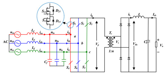
Figure 1.
The schematic diagram of three-phase isolated matrix converter.
From Figure 1, the structure of the grid side MC is equivalent to a conventional current source rectifier, except that the MC uses the bidirectional switches, and therefore, the conventional SVPWM can be adopted to control this converter [23]. In general, the reference vector is synthesized by two adjacent active vectors , and one zero vector (here, as shown in Figure 2). In order to maintain the flux balanced in HFT [24], the average voltage vector over a switching cycle is zero. Therefore, the switching vectors should produce an alternating positive and negative primary voltage of the HFT. Consequently, two switching states depending on the direction of the primary side current Ip for each vector are required to correspond to the positive and negative current vector, respectively. The current space vector distribution in the two cases of Ip > 0 and Ip < 0 is shown in Figure 2, and the switching state and the corresponding output voltage are listed in Table 1.
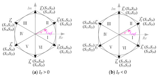
Figure 2.
Current space vector. (a) Ip > 0 (b) Ip < 0.

Table 1.
The corresponding switch state of the space vector.
2.2. DC-Link Current Ripple Analysis of Traditional Scheme
According to the formula , the expression of DC-link inductor current ripple can be expressed as:
where Udc is the bridge output voltage, Uo is the output voltage, and Δt is the charging/discharging time of inductor current.
From (1), it can be observed that the DC-link current ripple depends on the variable of Udc, which is associated with the switching states of the MC. Therefore, the inductor current ripple can be optimized through the above formula.
Take Sector І for example: can be represented by , , and , as shown in Figure 3.
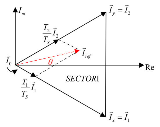
Figure 3.
Synthesis principle of reference vector Iref.
According to the ampere-balance principle in (2), the dwell times for three vectors can be obtained as (3)
where Ts is the sampling period, ma is the modulation index, and θ denotes the vector angle ().
The different vector sequence arrangements are well described in [22]. For the analysis in this paper, in order to avoid magnetic saturation caused by dc component, the transformer of the current mode matrix converter should ensure that the current with equal size and opposite phase passes through the primary side of the transformer in one cycle. In the positive half-cycle, I1 and I2 act, and the primary side output voltage of the transformer is VAB and VAC, respectively. In order to ensure that in the negative half-cycle, the action time of I4 is the same as I1, and the action time of I5 is the same as I2, the primary side voltage of the transformer is VBA and VCA, respectively. The traditional six-segment SVPWM scheme with a step change in the primary voltage of the HFT from a higher voltage amplitude to a lower one (HTL) is adopted. The output voltage of the primary side of the transformer and the corresponding switching states are shown in Figure 4.
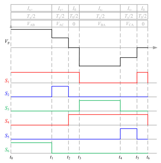
Figure 4.
Waveforms of the transformer primary voltage and switching states.
According to the above analysis, when the reference vector is located in Sector 1, the time-domain expression of DC-link current ripple can be calculated as (4).
From (4), the increasing/decreasing trend of the current ripple can be drawn in Figure 5a, where the traditional scheme is used, and this methodology is highlighted on page 4. Note that (4) is monotonic, and the peak–peak value of the DC-link current ripple is determined by , which can be defined as
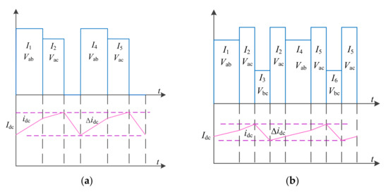
Figure 5.
Waveforms of the inductor current ripple. (a) Traditional scheme (b) Proposed scheme.
As shown in the previous analysis, the current ripple of the traditional six-segment SVPWM scheme with HTL is not optimized.
3. Proposed Solution
As shown in the previous section, it is hard to reduce the DC-link current ripple with conventional SVPWM by synthesizing the reference vector with two adjacent active vectors ,, and one zero vector. In order to reduce the DC-link current ripple effectively, the space vector is divided into 12 sectors, as shown in Figure 6. In this section, an optimal scheme is proposed by employing six non-nearest vectors in each sector to synthesize the reference vector to solve the above problem.
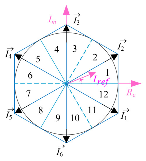
Figure 6.
New current space vector diagram.
Table 2 shows the current vectors, switching sequence, and the corresponding primary side voltage of the HFT. It indicates that the primary side voltage is determined by the current vectors and line voltage. Figure 7 shows the relationship of the bridge output voltage Udc, the amplitude of line–line voltage Vi, and the vector angle θ of the reference vector. From Figure 7, the line–line voltage in each sector is monotonic. From (1), the DC-link current ripple Δi can be optimized depending on the bridge output voltage Udc, which is determined by the switching states, as shown in Table 2; that is, the DC-link current ripple would be high if Udc steps from the highest to lowest one depending on the vector sequence.
Table 2.
The corresponding switching sequence and the output voltage.
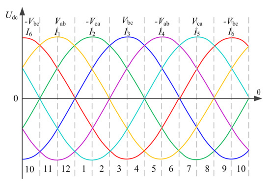
Figure 7.
Line voltage and sector division.
Taking the range of −30° to 30° as an example, and assuming that the current reference is located in sector 1, which is shown in Figure 8, the DC-link current ripple would be decided by the vector sequence. The vector sequence of the traditional modulation scheme is , and the corresponding Udc would be Vab, Vac, 0 and Vac > Vab > 0; consequently, the high current ripple would be caused by Udc steps from the highest line-line voltage to 0 when . In order to solve the problem, an optimum scheme with the main idea to synthesize the current reference vector with available non-nearest vectors is proposed. Instead of using zero vector and guaranteeing only one switch action when the vector changes, the proposed solution used the optimum vector sequence , and the maximum step change of Udc can be avoided. Therefore, compared with the conventional solution, the proposed scheme can significantly reduce the DC-link current ripple. Next, a detailed theoretical analysis will be derived.
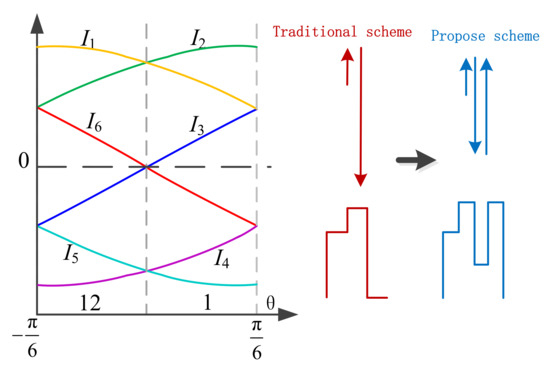
Figure 8.
Relationship of variables in sector 12 and sector 1.
Different from the conventional current source rectifier, the primary side voltage of the HFT must be alternating positive and negative to maintain the volt-sec balance. Therefore, taking reference vector located in sector 1, for example, three active vectors I1, I2, and I3 are used in the positive half-cycle, and the active vectors I4, I5, and I6 are used in the negative half-cycle. Based on the above analysis, Table 3 shows the corresponding relationship between the 12 sectors and the vector sequence.
Table 3.
New scheme partition and vector action sequence.
When the reference vector is located in the odd sector (1, 3, 5, 7, 9, 11), the dwell times of each vector can be calculated by
When the reference vector is located in the odd sector (2, 4, 6, 8, 10, 12), the dwell times of each vector can be calculated by
By combining (1) and (6)–(7), the DC-link current ripple can therefore be calculated in (8). Additionally, Figure 5b shows the increasing/decreasing trend of the current ripple of the proposed scheme.
From (8) and Figure 5b, the peak–peak value of the DC-link current ripple of the proposed scheme can be defined as
As shown in Figure 5, it can be observed that the proposed solution can effectively mitigate the DC-link current ripple compared with the conventional solution.
Figure 9 shows the control algorithm, which can be summarized into the following seven steps:
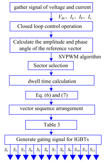
Figure 9.
Control algorithm.
4. Simulation Results
In order to verify the effectiveness of the theoretical analysis, comparative simulations in MATLAB/Simulink with the proposed SVPWM strategy and the conventional scheme for the three-phase isolated matrix converter are carried out. The MATLAB/ Simulink model consists of the main circuit and control module, where the IGBT is used for the main circuit of matrix converter, and the S-function is used to implement the control module of space vector modulation algorithm, as shown in Figure 10. The simulation parameters are listed in Table 4.
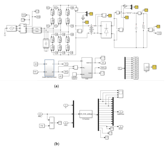
Figure 10.
MATLAB/Simulink model. (a) Main circuit and control module. (b) S-function of SVPWM.
Table 4.
Parameters of simulation model.
Figure 11 shows the rectifier bridge output voltage and DC-link current ripple waveforms under the different inductance values. It can be observed that the traditional modulation scheme produces a large DC-link current ripple when Udc steps from the highest line voltage to 0. On the contrary, the proposed solution employs the optimum vector sequence, which can effectively avoid the maximum step change of Udc. As a consequence, the DC-link ripple of the proposed solution is much lower than that of the conventional one.
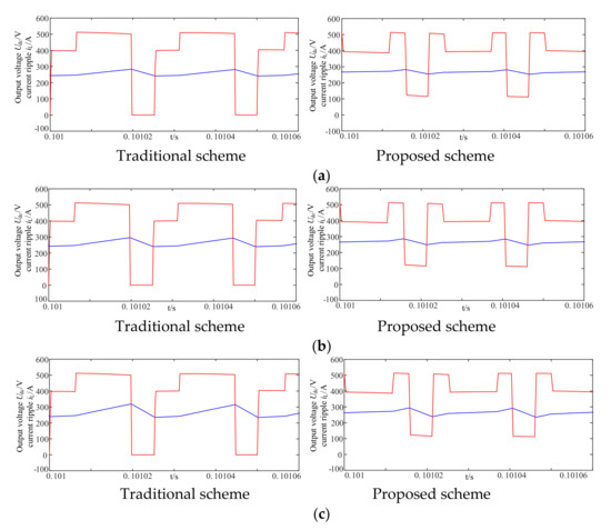
Figure 11.
Rectifier bridge output voltage and inductor current ripple. (a) Inductance with 2 mH (b) Inductance with 1.5 mH (c) Inductance with 1 mH.
Figure 12 shows the filter inductor current waveforms under the different inductance values. It can be clearly seen that the peak-to-peak current ripples of the traditional scheme are 2.07 A, 1.32 A, and 1 A at 1 mH, 1.5 mH, and 2 mH inductance values, respectively. From Figure 12b, the peak-to-peak current ripple of the proposed scheme are 1.36 A, 0.9 A, and 0.68 A with corresponding inductance values; that is to say, the maximum DC-link ripple of the proposed scheme is much lower than that of the conventional one. It is also noted that the smaller the inductance, the better the current ripple reduction.
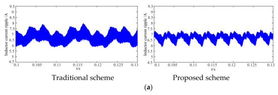
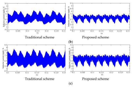
Figure 12.
DC output filter inductor current waveform. (a) Inductance with 2 mH (b) Inductance with 1.5 mH (c) Inductance with 1 mH.
For analysis of simulation, it can be seen that compared with the traditional scheme, the new scheme can reduce the DC-side inductance current ripple only by changing the modulation strategy without increasing the inductance value and switching frequency.
For easier viewing, the peak-to-peak current ripple of the traditional scheme and the proposed scheme with different inductance values are summarized in Figure 13. It can be observed that the proposed scheme can effectively reduce peak-to-peak current ripple compared with the conventional solution. In other words, for a given current ripple requirement, the DC-link inductor can be designed as a smaller size and lower inductance and cost.
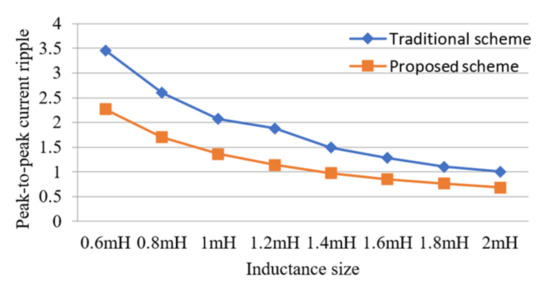
Figure 13.
Current ripple with different inductance values.
5. Experimental Results
To verify the proposed SVPWM strategy for the three-phase isolated matrix converter, a lab prototype is built, as shown in Figure 14. Texas Instruments DSP TMS320F28335 and FPGA XC6SLX9-2TQG144C are used to implement the control algorithm. Detailed parameters of the experiment are listed in Table 5.
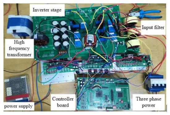
Figure 14.
Experimental setup.
Table 5.
Experimental parameters.
Figure 15 and Figure 16 show the experimental waveforms of the conventional SVPWM. The overall and detailed enlarged waveforms of the primary and secondary voltages of the transformer are shown in Figure 15, and it can be seen that the measured waveforms of the primary and secondary voltages of the transformer step from a higher voltage amplitude to a lower one and they are characterized by the alternatively positive and negative variations. It is also noted that the voltage amplitudes of the primary and secondary sides are approximately the same since the transformer ratio is designed to be 1:1. Figure 16 shows the experimental waveforms of the output voltage and DC-link inductor current with the conventional solution. The current ripple is large since the SVPWM modulation is not optimized.
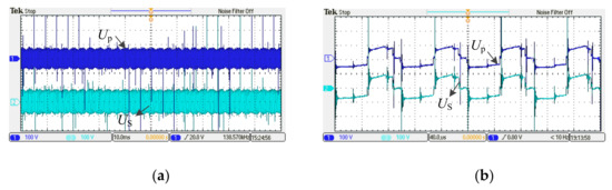
Figure 15.
Experimental results with conventional solution. (a) Overall waveform (b) Detail waveform.
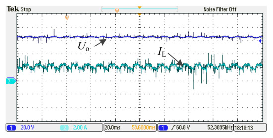
Figure 16.
Output voltage and inductor current with conventional solution.
Figure 17 shows the experimental comparison of the conventional and proposed solutions from the viewpoint of the rectifier bridge output voltage and DC-link current ripple. The experimental parameters are listed in Table 5. It can be seen that the DC-link current ripple has been reduced from 0.5 A (conventional scheme) to 0.3 A (proposed scheme), and the corresponding current ripple factors are 45.4% and 27.3%, respectively. Consequently, the experimental results verify the effectiveness of the proposed strategy that can significantly reduce the DC-link current ripple, which is in agreement with the theoretical analysis in Figure 12.
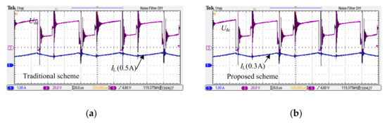
Figure 17.
Comparison waveforms of conventional and proposed schemes. (a) Traditional scheme (b) Proposed scheme.
6. Conclusions
This paper presented an optimized SVPWM by using the active vector instead of the zero vector to reduce the DC-side inductor current ripple for the three-phase isolated converter. After theoretical analysis, simulation, and experimental verification, the following conclusions are obtained. Different from the traditional modulation schemes, the proposed solution can effectively reduce the current ripple. On the other hand, the application of large filter inductance is avoided. Aside from that, the proposed scheme can be easily implemented without increasing the switching frequency or adding any other hardware. Therefore, the proposed scheme is attractive for three-phase isolated converter applications.
Author Contributions
All authors contributed to this work by collaboration. All authors have read and agreed to the published version of the manuscript.
Funding
This work was supported in part by the National Natural Science Foundation of China under Grant 61903321, Hebei Province 333 Talent Program (A202005001), and the Foundation of Hebei Educational Department QN2019016.
Institutional Review Board Statement
Not applicable.
Data Availability Statement
Not applicable.
Conflicts of Interest
The authors declare no conflict of interest.
Nomenclature
| SVPWM | Space vector pulse width modulation |
| FACTS | Flexible ac transmission system |
| FPGA | Field-programmable gate array |
| IGBT | Insulated gate bipolar transistor |
| HVDC | High voltage direct current |
| HFT | High-frequency transformer |
| THD | Total harmonic distortion |
| DSP | Digital signal processor |
| MC | Matrix converter |
References
- Kadem, K.; Bensetti, M.; Le Bihan, Y.; Labouré, E.; Debbou, M. Optimal Coupler Topology for Dynamic Wireless Power Transfer for Electric Vehicle. Energies 2021, 14, 3983. [Google Scholar] [CrossRef]
- Monjo, L.; Sainz, L.; Mesas, J.J.; Pedra, J. State-Space Model of Quasi-Z-Source Inverter-PV Systems for Transient Dynamics Studies and Network Stability Assessment. Energies 2021, 14, 4150. [Google Scholar]
- Xiao, G.; Na, W.; Bao, W.; Lu, Z.; Frede, B. Evaluation of Three-Phase Transformerless DC-Bypass PV Inverters for Leakage Current Reduction. IEEE Trans. Power. Electron. 2020, 35, 5918–5927. [Google Scholar]
- Duran, A.; Ibaceta, E.; Diaz, M.; Rojas, F.; Cardenas, R.; Chavez, H. Control of a Modular Multilevel Matrix Converter for Unified Power Flow Controller Applications. Energies 2020, 13, 953. [Google Scholar] [CrossRef] [Green Version]
- Casadei, D.; Serra, G.; Tani, A.; Zari, L. Matrix Converter Modulation Strategies: A New General Approach Based on Space-Vector Representation of The Switching State. IEEE Trans. Ind. Electron. 2002, 49, 370–381. [Google Scholar] [CrossRef]
- Nguyen, T.D.; Lee, H. Modulation Strategies to Reduce Common-Mode Voltage for Indirect Matrix converters. IEEE Trans. Ind. Electron. 2012, 59, 129–140. [Google Scholar] [CrossRef]
- Rivera, M.; Wilson, A.; Rojas, C.A.; Rodrigez, J.; Espinoza, J.R.; Wheeler, P.W.; Empringham, L. A Comparative Assessment Of Model Predictive Current Control And Space Vector Modulation In A Direct Matrix Converter. IEEE Trans. Ind. Electron. 2013, 60, 578–588. [Google Scholar] [CrossRef]
- Rodriguez, J.; Rivera, M.; Kolar, J.W.; Wheeler, P.W. A Review of Control and Modulation Methods for Matrix Converters. IEEE Trans. Ind. Electron. 2012, 59, 58–70. [Google Scholar] [CrossRef]
- Alesina, A.; Venturini, M.G.B. Analysis and Design of Optimum-Amplitude Nine-Switch Direct AC-AC Converter. IEEE Trans. Power. Electron. 1989, 4, 101–112. [Google Scholar] [CrossRef]
- Vazquez, S.; Lukic, S.M.; Galvan, E.; Franquelo, L.G.; Carrasco, J.M. Energy Storage Systems For Transport and Grid Applications. IEEE Trans. Ind. Electron. 2010, 57, 3881–3895. [Google Scholar] [CrossRef] [Green Version]
- Bhuiyan, F.A.; Yazdani, A. Energy Storage Technologies for Grid Connected and Off-Grid Power System Applications. In Proceedings of the IEEE Electrical Power and Energy Conference, London, ON, Canada, 10–12 October 2012; pp. 303–310. [Google Scholar]
- Al-Tameemi, M.; Miura, Y.; Liu, J.; Bevrani, H.; Ise, T. A Novel Control Scheme for Multi-Terminal Low-Frequency AC Electrical Energy Transmission Systems Using Modular Multilevel Matrix Converters and Virtual Synchronous Generator Concept. Energies 2020, 13, 747. [Google Scholar] [CrossRef] [Green Version]
- Yilmaz, M.; Krein, P. Review of Battery Charger Topologies, Charging Power Levels and Infrastructure for Plug-In Electric and Hybrid Vehicles. IEEE Trans. Power Electron. 2013, 28, 2151–2169. [Google Scholar] [CrossRef]
- Afsharian, J.; David, X.; Gong, B.; Yang, Z. Space Vector Demonstration And Analysis Of Zero-Voltage Switching Transitions In Three-Phase Isolated PWM Rectifier. In Proceedings of the IEEE Energy Conversion Congress and Exposition, Montreal, QC, Canada, 20–24 September 2015; pp. 2477–2484. [Google Scholar]
- Feng, B.; Lin, H.; Wang, X.; An, X.; Liu, B. Optimal Zero-Vector Configuration For Space Vector Modulated AC-DC Matrix Converter. In Proceedings of the IEEE Energy Conversion Congress and Exposition, Montreal, CA, Canada, 20–24 September 2012; pp. 291–297. [Google Scholar]
- Baumann, M.; Kolar, J. Minimization of the Dc Current Ripple of a Three-Phase Buck-Boost PWM Unity Power Factor Rectifier. In Proceedings of the Power Conversion Conference-Osaka 2002, Osaka, Japan, 2–5 April 2002; pp. 472–477. [Google Scholar]
- Guo, X.; Yang, Y.; Wang, X. Optimal Space Vector Modulation of Current Source Converter for DC Link Current Ripple Reduction. IEEE Trans. Ind. Electron. 2019, 66, 1671–1680. [Google Scholar] [CrossRef]
- Shuai, D.; Zhang, Q.; Cheng, S. Inductor Current Ripple Comparison between ZSVM4 and ZSVM2 for Z-source Inverters. IEEE Trans. Power. Electron. 2016, 31, 7592–7597. [Google Scholar]
- He, Y.; Xu, Y.; Chen, J. New Space Vector Modulation Strategies to Reduce Inductor Current Ripple of Z-source Inverters. IEEE Trans. Power. Electron. 2018, 33, 2643–2654. [Google Scholar] [CrossRef]
- Guo, X.; Xu, D.; Guerrero, J.M.; Wu, B. Space Vector Modulation For Dc-Link Current Ripple Reduction In Back-To-Back Current-Source Converters For Microgrid Applications. IEEE Trans. Ind. Electron. 2015, 62, 6008–6013. [Google Scholar] [CrossRef]
- Afsharian, J.; Xu, D.; Gong, B.; Yang, Z. Reduced Duty-Cycle Loss and Output Inductor Current Ripple in A ZVS Switched Three-Phase Isolated PWM Rectifier. In Proceedings of the IEEE Applied Power Electronics Conference and Exposition, Long Beach, CA, USA, 20–24 March 2016; pp. 33–37. [Google Scholar]
- Afsharian, J.; Xu, D.; Wu, B.; Gong, B.; Yang, Z. The Optimal PWM Modulation and Commutation Scheme For A Three-Phase Isolated Buck Matrix-Type Rectifier. IEEE Trans. Power Electron. 2018, 33, 110–124. [Google Scholar] [CrossRef]
- Li, X.; Wu, F.; Yang, G.; Liu, H.; Meng, F. Precise Calculation Method of Vector Dwell Times for Single-Stage Isolated Three-Phase Buck-Type Rectifier to Reduce Grid Current Distortions. IEEE Emerg. Sel. Top. Power Electron. 2020, 8, 4457–4466. [Google Scholar] [CrossRef]
- Fang, F.; Tian, H.; Li, Y. Coordination Control of Modulation Index and Phase Shift Angle for Current Stress Reduction in Isolated AC–DC Matrix Converter. IEEE Trans. Power Electron. 2021, 36, 4585–4596. [Google Scholar] [CrossRef]
Publisher’s Note: MDPI stays neutral with regard to jurisdictional claims in published maps and institutional affiliations. |
© 2021 by the authors. Licensee MDPI, Basel, Switzerland. This article is an open access article distributed under the terms and conditions of the Creative Commons Attribution (CC BY) license (https://creativecommons.org/licenses/by/4.0/).