Review

An Overview of Fully Integrated Switching Power Converters Based on Switched-Capacitor versus Inductive Approach and Their Advanced Control Aspects

1
School of Electrical Engineering, VIT Vellore, Tamil Nadu 632014, India
2
School of Electrical Sciences, IIT Goa, Ponda 403401, India
3
Department of Energy Technology, Aalborg University, 9220 Aalborg, Denmark
4
TIFAC-CORE, VIT Vellore, Tamil Nadu 632014, India
*
Author to whom correspondence should be addressed.
Energies 2021, 14(11), 3250; https://doi.org/10.3390/en14113250
Submission received: 18 April 2021 / Revised: 10 May 2021 / Accepted: 27 May 2021 / Published: 2 June 2021
(This article belongs to the Special Issue Current Researches on Integrated DC/DC Converters)

Abstract

:
This paper reviews and discusses the state of the art of integrated switched-capacitor and integrated inductive power converters and provides a perspective on progress towards the realization of efficient and fully integrated DC–DC power conversion. A comparative assessment has been presented to review the salient features in the utilization of transistor technology between the switched-capacitor and switched inductor converter-based approaches. First, applications that drive the need for integrated switching power converters are introduced, and further implementation issues to be addressed also are discussed. Second, different control and modulation strategies applied to integrated switched-capacitor (voltage conversion ratio control, duty cycle control, switching frequency modulation, Ron modulation, and series low drop out) and inductive converters (pulse width modulation and pulse frequency modulation) are then discussed. Finally, a complete set of integrated power converters are related in terms of their conditions and operation metrics, thereby allowing a categorization to provide the suitability of converter technologies.

1. Introduction

With the advancements in integrated circuit technologies and computing, the demand for integrated power conversion, regulation, and its management functions is increasing in many applications, such as portable devices that alter one voltage level into another level, which can be accommodated in a limited volume. Small-volume voltage conversion and efficiency are the key features, as they allow the provision to host an additional number of features in portable devices such as notebook computers, cellular and cordless phones, and camcorders. Conventionally, two popular approaches exist to achieve the voltage conversion [1]. They are the linear regulator and switch-mode conversion. The linear regulator is a continuous time circuit and acts like a voltage divider network. It allows the voltage conversion, but only in step-down mode. The energy supplied from the input source is dissipated in the form of heat across the resistor element. On-the other hand, switch-mode regulators consist of a controllable switch and one or more energy storage elements, such as an inductor and a capacitor, which allow both step-up and step-down voltage conversions. When a capacitor is used, it is termed as ‘switched-capacitor converter’. Similarly, an inductor is used to yield a ‘switched inductive converter’. In comparison to inductors, energy density of capacitors is 100–1000 times more [2]. This makes Switched capacitor converters (SCCs) to be of excessive power-density converters and are accessible in reduced circuit volume [3,4].
The use of linear regulators is not a preferred choice in many applications to assist with voltage conversion due to their poor efficiency and a limitation of their output voltage Vo being less than input voltage Vin. In particular, when the voltage conversion ratio between Vo and Vin is large, the energy in the linear regulators gets dissipated and produce high temperatures in a small volume. On the other hand, switch-mode power converters became popular for exhibiting higher efficiencies along with the achievable desired voltage conversion ratio. The realization of switch-mode power converters utilizes reactive elements; i.e., inductors and/or capacitors. In recent times, the applications maintain a stringent requirement on small volume. In this direction, switch-mode power converters with a small form factor are gaining interest due to the addition of integrated reactive components; i.e., no external capacitors or inductors.
The objective of on-chip power distribution system is to supply the necessary current to the load through the whole chip, by keeping the required voltage level for suitable for the load. Low noise, efficient, and minimized power supply on-chip is needed for fully integrated system on-a-chip (SoC) arrangements [5,6,7,8]. With regard to the timely evolution of SOC functions that has maturely developed, switch-mode power conversion will be used. The efficient integrated power conversion, which is at an early stage, would be better suited for SOC functions than switch-mode power conversion, owing to smaller volume. The present trend in multicore processors is to use many individually controlled voltage rails and dissipate the power around 1 W/mm2. An integrated DC–DC conversion would possibly serve as a desired benchmark, and requires a regulation such that: (1) higher efficiency can be maintained over a wide range of operating conditions; (2) it affords tight regulation; (3) it can hold power around 10 W/mm2; (4) it reduces to a voltage below the CMOS (Complementary Metal Oxide Semiconductor) core voltage that it can handle; (5) it is suitable for granular implementation [9].
In the modern era, digital ICs are gaining more attention due to their low power consumption, and they increase the necessity of usage of the integrated switch-mode power converters. Further, voltage-scaling and body-bias techniques reduce the power consumption of digital circuits [10,11,12]. For performing voltage scaling, the digital circuit is segregated into separate voltage islands with distinct voltage rails to reduce their power consumption without sacrificing the desired performance. Body-bias techniques modify the circuit behavior and require step-up/down conversion, or voltage inversion. By raising the threshold voltage level, the gate discharge of a transistor can be reduced when a reverse body bias is supplied, and this decreases the discharge of the digital circuit during idle operation. Forward body bias makes the digital circuit operate in active mode. This improves both speed and performance for a smaller value of threshold voltage. The output power range of an integrated downconverter, either switched-inductive or capacitor with voltage scaling, lies around 100–400 mW for subthreshold processors [13]. In comparison to inductive converters, switched-capacitor converters are more suitable for integration, as they need the lower output power of body-bias voltage generators.
The amalgamation of a power converter with a load is desirable in reducing the space and delivering enhanced power quality. The integrated switching power converters are synthesized in the nanometer range for CMOS IC processes in voltage scaling and body-bias voltage generation. The integration of reactive elements becomes more complex in nanometer CMOS processes, as it demands high cost/area with low energy-storage density. In the process of reducing the silicon area, the integration follows two major approaches. First and foremost is a system-in package (SiP) approach that uses a committed technology for integrating the reactive components. In the second approach, the reactive elements are added on the same die followed by the postprocessing procedure.
In comparison to the nonintegrated switch-mode power converters, the integration process produces smaller capacitance and inductance densities. As a consequence, the switching frequencies of integrated switching power converters are quite high. This implies a trade-off between the efficiency and the area occupied by the reactive elements (switching frequency), which plays a crucial role in the design of integrated power converters. The design is carried out in such a way that integrated switch-mode power converters produce more efficiency than linear regulators.
This paper provides an overview of integrated switching converters. The following sections emphasize integrated switched capacitors and switched-inductor converters and their modelling, efficiency and power-loss distributions, control techniques, and integration technology options. Lastly, a comparison between integrated switched capacitors and inductors using the performance metrics are discussed, and then the conclusions are presented.

2. Integrated SC Converters

Applications that necessitate SC converters such as flash and EEPROM memories are generally used in low power, and high input voltage. They reduce the quantity of external supplies, larger voltages from battery sources [14,15,16], high side switch drivers [17]. A new single input SC-based (2n + 1)-level inverter has been presented in [18] with boost capability. The proposed topology features many advantages when compared with various suggested single-input, SC-based (2n + 1)-level inverter topologies, namely scalability, utilization of a low number of semiconductors, low voltage stress, high efficiency and power density, low cost and size, and simple modulation control. The following section briefly describes the integrated switched-capacitor (SC) converters based on averaged modeling, efficiency, and power-loss distribution; multiratio switched-capacitor converters (MR-SCPCs); and control strategies applied to integrated SC converters, multiphase SC converters, and technology options for SC converters.

2.1. SC Converter Average Modelling

The steady-state model of SC converter can be represented using an ideal transformer with series output impedance, after neglecting the parasitic losses, which are frequency-dependent. Even so, the SC converters exhibit time-varying behavior, and their models can be represented using an ideal transformer and a series resistance at the output terminals, as shown in Figure 1a [19,20].
The SC converter’s topology determines the voltage conversion ratio M of the transformer, where the capacitors are placed at various phases to form a new circuit. The average equivalent output resistance of an SCPC is denoted with Rout, which depends on the switching frequency fs, the capacitance value of floating capacitors, the ON state resistance of the respective switches Ron, and the duty cycle. To a lesser extent, the secondary effects, such as dead time of switching pulses, parasitic resistance of the floating capacitors, and their connections, also vary the output resistance. Subsequently, such variation affects the output voltage Vo.
For a given number of floating capacitors, an SCPC was proposed using all the positive conversion ratios available in 1995 [21]. All the possible voltage conversion ratios of the transformer can be determined from the following equation:
M = P [ k ] Q [ k ]
where P[k] represents the positive integers and Q[k] represents the ‘k’ elements of the Fibonacci series (2 ≤ k ≤ (N + 1). ‘N’ represents the number of capacitors together with the output capacitor Cout. For different numbers of floating capacitors, possible conversion ratios are given in Table 1. All the possible conversion ratios of the SC converter were established by the theorem presented in [21].
The SCPC operates either in slow switching limit (SSL) or in fast switching limit (FSL), or in between them. When the SCPC is operated at a low/high switching frequency, its behavior is termed as SFL/FSL. In the SSL operating region, the amount of charge that can be transferred by capacitors dominates the SCPC losses and output impedance. In the FSL operating region, Ron dominates the converter losses, as it restricts the capacitors from transferring the charge completely in each switching period.
It was pointed out in [21] that the output resistance of SCPC (Rout) is a function of the switching frequency, as shown in Figure 1b, and it can be inferred that Rout behaves asymptotically different at low and high switching frequencies. Its value can be found from the square root of the sum of the squared asymptotic values. However, Ref. [20] proposed a simple yet systematic approach to model the Rout in the case of a two-phase SCPC. This method depends on SSL and FSL operating regions that correspond to asymptotically different characteristics, as pointed out in [19]. Based on this model, the approximated value of Rout can be found from the following:
R out = R 2 FSL + R 2 SSL
where RFSL and RSSL represent the FSL and SSL limits as shown in Figure 1b, respectively. Considering a 50% duty cycle in coherence to the clock signal, the capacitance C, which is the sum of all floating capacitances, and assuming the same Ron for all switches, the values of RFSL and RSSL are calculated as follows:
R SSL = m f s C   ;   R FSL = pR on
where m and p are the positive integers. For the same voltage conversion ratio M, m and p behavior changes w.r.t the topology. For example, two circuit topologies with M = 0.25 exhibit different output impedances, as shown in Figure 2.
When parameters such as switching frequency and component sizes are excluded, an optimized design can be achieved around the corner frequency (fc), where SSL and FSL limits cross. This is shown in Figure 1b, and it can be observed that a higher switching frequency causes the increase in switching losses without decreasing Rout. Similarly, for a higher Rout, small floating capacitors are preferred in integrated implementations. Further, for applications in which output-voltage regulation is required, the design should provide a smaller value of Rout, and an additional degree of freedom is provided if the lowest value of Rout is around the corner frequency.

2.2. Efficiency and Power-Loss Distribution

The difference between the low drop out (LDO) and VinM gives the average output voltage Vo of SCPC converter as shown in Figure 1a. Neglecting the switching losses, the efficiency of an ideal SCPC is given by following relation
η theoretical = V o MV in
In applications with wide variation in Vin and/or Vo, obtaining the acceptable efficiency is a nontrivial task unless Vo approaches VinM.
As mentioned previously, conduction losses denoted with Pcond contribute majorly to loss calculation, and are represented using Rout in the averaged model of SCPC. The design process is initiated after fixing the voltage conversion ratio M and the combination of input, output voltages, and output current fixes the conduction losses Pcond. This is given as follows:
P cond = ( MV in V o ) × I o
where Io represents the output current. In the FSL region of operation, the conduction losses hold a proportional relationship with the on-state resistance of switches Ron. On the other hand, they do not depend on each other in SSL operation. These relations are shown in Equation (3). An important observation is that in both SSL and FSL operations, the power is dissipated due to the on-state resistance of switches and the parasitic resistance. This illustrates the reason behind Pcond losses for both the SSL and FSL limits. After selecting the suitable voltage conversion ratio M and using Equation (4) as the upper limit for the efficiency, the switching losses Psw are computed. These are classified into the following two categories.

2.2.1. Bottom-Plate Losses

As the circuit phase changes, the energy is wasted in charging and discharging the capacitances at the ends of floating capacitors of the SCPC, and this waste contributes to these switching losses. These losses are mainly due to the common planar nature of integrated capacitors, and are mainly associated with the top and bottom plates of parasitic capacitances, as well as the junction capacitance between the drain-source terminals of switches. Bottom-plate losses contribute in large extent to switching losses, even though they greatly depend on technology. For the same voltage conversion ratio M, different topologies produce bottom-plate losses in different amounts; this is addressed in [22,23]. Moreover, Ref. [22] developed a switching scheme to decrease the amount of these losses.

2.2.2. Driver Losses

Typically, the drivers are realized by tapered buffers in CMOS technologies, and the energy wasted in the drivers of power switches belongs to this category. With an optimized design, the total switching losses can be reduced if the driver circuits are designed alongside the respective switches [24].

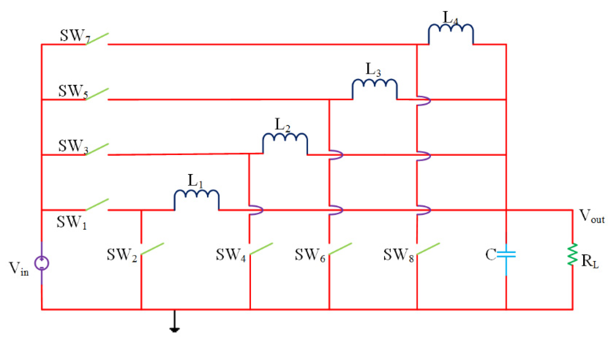
2.3. Multiratio SC Power Converters (MR-SCPC)

The applications that demand a wide range of variations in Vin and/or Vo values would result in poor efficiency when an SCPC is employed. In order to enhance the efficiency, the multiratio SCPC (MR-SCPC) would be a suitable choice. Neglecting the switching losses, making Rout = 0 Ω at the peaks, the efficiency of various topologies of SCPC with one, two, or three floating capacitors is shown in Figure 3 [25]. It shows that for wide variations in Vin and/or Vo, employing MR-SCPC would provide additional benefits. Several researchers suggest using an integrated SCPC to implement as an MR-SCPC [26,27,28,29].
The multiratio configuration is less efficient than expected, as there is an increase in the number of components such as drivers and switches, which provides inadequate low output impedance and affects the peak of waveforms, as shown in Figure 3. The efficiency as a function of current density is shown in Figure 4 for two MR-SCPCs with N = 3 and N = 4. To take full advantage of the average efficiency throughout the Vin range, the designs are improved at every stage. It can be noticed from Figure 4 that the enhancement in the efficiency with a multiratio structure becomes clearly visible only for low power densities that use relatively low switching frequencies. Under these circumstances, the efficiency majorly depends on conduction losses, which need to be reduced by using a larger M from the available choices.

2.4. Integrated SC Converter Control Schemes

Excluding the conversion ratio control, a majority of the control techniques provide the controlling action for adjusting the voltage through the alteration of Rout, similar to a linear regulator. According to Equation (5), the conduction losses Pcond can be found using the SCPC topology. Hence, the variation in the efficiency for smaller values of Io is related to the controller for minimizing the switching losses Psw. The integrated SCPC requires closed-loop controllers to achieve the line and load regulation, and in view of this, there are several control schemes available despite the complex nature of the output impedance of an SCPC. A brief description is provided below.

2.4.1. Conversion Ratio Control

This technique tunes the voltage conversion ratio M to maintain the desired output voltage, and this further allows reducing the conduction losses. However, M takes only discrete values, and the output resistance Rout varies nonlinearly as the SCPC topology changes. Due to this, the majority of the designs alter the topology in an open loop based on Vin and Vo, instead of including the drop associated with IoRout in a closed loop [13,22,26,27,28]. However, M of an SCPC topology is controlled in a closed loop after sensing the load current Io, even though the topology is not fully integrated [30,31]. As the adequate M values are not available, these topologies are combined with various control schemes to maintain a fine regulation. The value of switching frequency does not vary, and produces noise in the expected spectrum.

2.4.2. Duty-Cycle Control

Under the constant frequency operation, the ON time duration of the switches is varied to control the output voltage for the changes in load current. This control approach effectively changes the series resistance of the charge-transfer switches, RFSL. This in turn varies the quantity of charge transferred to the load in each cycle. The duty-cycle control scheme depends on the RFSL value, as RFSL is a function of the duty ratio. When fixing the duty ratio to 50%, the minimum RFSL value is determined. However, this does not enhance the efficiency, as the switching activity is not related to the output power. As a result, the switching losses become constant for the complete range of load current [32] Io, and this produces a noise in the expected spectrum. The duty-cycle control is integrated with programmable fs to minimize the switching losses at low power [33,34].

2.4.3. Switching Frequency Modulation

The use of frequency-modulation techniques such as PFM for hysteresis control in the majority of control schemes linked with SCPC are favored, as they minimize Psw, which is proportional to Io [35,36,37]. This provides invariable efficiency η = f(Io). The main limitation of this frequency modulation comes from the noise produced, which is result of switching frequency modulation to attain the desired regulation. The switching frequency modulation is beneficial in digital systems like wireless applications [32].

2.4.4. Ron Modulation

This method uses the ON-state resistance of the switches to regulate the output voltage of an SCPC in the presence of changes in the input voltage and output current, particularly in FSL designs. There are two ways for altering the Ron if the switches are realized with MOS transistors, and they are as follows:
(1)
The width of MOS transistor is varied using segmented switches [26]. This mechanism has a limitation in that it only works with the discrete Ron values and produces a complex control signals for routing.
(2)
The second mechanism uses the Ron for modulating the Vgs voltage of a MOS (METAL OXIDE SEMICONDUCTOR) transistor. It generates the uninterrupted values for the complete ON duration of the switch. However, the strong nonlinearity between the Ids and Vgs makes the control loop unstable, whenever Vgs approaches the threshold voltage. For example, Ref. [31] used the transistor as a switch in an SCPC.
These two mechanisms for altering the ON-state resistance produces the switching losses due to the power dissipated in the drive, which is a squared function of variation in the applied voltage. Thus, the control logic for Ron modulation reduces the switching losses without disturbing the fs. This feature is attractive for noise-sensitive applications.

2.4.5. Series LDO

The series connection of an LDO with an SCPC is a frequently used method, as it adopts a simple approach [38,39]. The basic idea in this method is to maintain the voltage difference between the input and output voltages using an SCPC, and control the output voltage using a series-connected LDO. When an LDO is connected to the input/output terminals of an SCPC, it minimizes the input current/output voltage ripples, respectively. Moreover, faster dynamics can be obtained for controlling the load. The major limitation of this method is that it demands a higher switching frequency to allow the smaller voltage drop across the LDO when compared to the IoRout drop of the SCPC. As a result, this method increases the size of capacitors and ratings of switches, or both, and this increases the switching losses Psw.

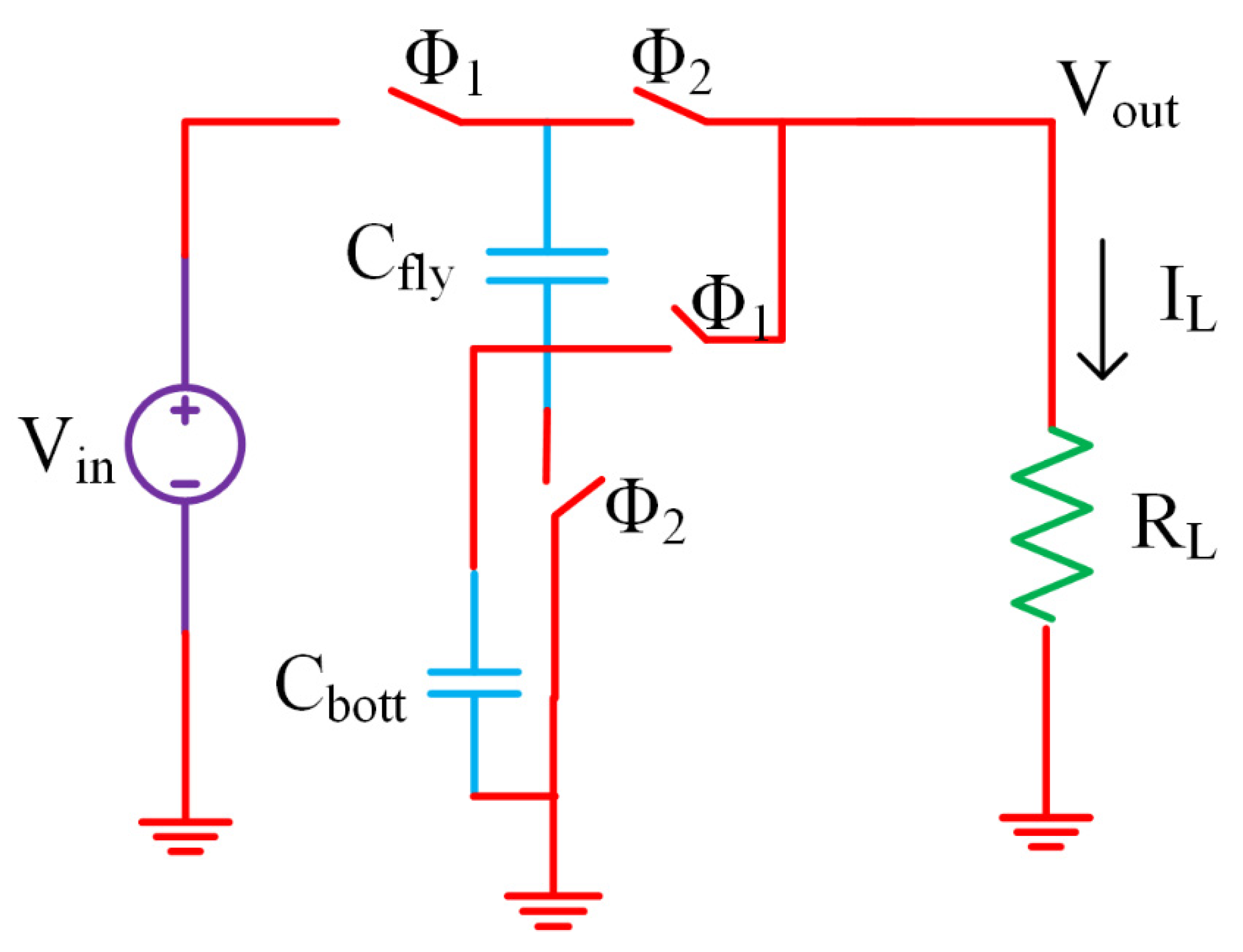
2.4.6. Floating-Capacitor Size Modulation

This method maintains the switching losses Psw in proportion to the load current without altering the switching frequency fs. The aim is to divide the number of floating capacitors into smaller numbers, such that only the desired amount of floating capacitors is used at various levels of output power [32]. This affects the number of bottom plates. When the same idea is applied to SCPC in dividing the number of floating capacitors and switches, the split portions can be used as estranged parallel modules [27]. The sizing of the split modules determines the amount of change in the efficiency as a function of load current and the change in output voltage ripple for a fixed-output capacitor. The resulting discrete values of applied output power cause cycle-limit behavior, which requires additional techniques to regulate. The significant benefit of this strategy is that the switch width is selected to fit in size of the capacitance.
A qualitative comparison is provided below. All the above control strategies discussed with switching, conduction losses, and noise are shown in Table 2. In addition, availability of a continuous/discrete regulation of output voltage Vo is provided. Hence, it can be concluded that a combination of different control strategies is required to get several advantages [13,27,32,33,37].
From Table 2, it can be observed that the series LDO control technique reduces the noise, but has more switching losses. Switching frequency modulation enhances the noise, but has low switching losses. Both Ron modulations (Vgs and Wch) have low switching losses and noise. Capacitor size modulation has very low switching losses and also reduces the noise. Therefore, it can be concluded that capacitor size modulation brings significant improvements, as it reduces both the switching losses and noise.

2.5. Multiphase SC Power Converters (MP-SCPC)

A single SCPC is divided into numerous smaller SCPCs in a modular approach, which leads to a multiphase SCPC (MP-SCPC) [26,28,29,35,36,40,41], and their clock phases are uniformly shared throughout the entire switching period. The output voltage ripple will be reduced because at different time constants, the charge is applied to the output with the help of small charge packages. By doing so, the input current shows a smaller ripple when the charge is taken in small packages from the input source voltage. As a consequence, the noise generated is of a lower value. The size of Cout gets reduced at the output node when the charge is injected at one or fewer phases, and this further remarkably reduces the size of the integrated SCPC.
Furthermore, the control of the number of MP-SCPC active converters will deliver a constant efficiency as a function of Io. Nevertheless, the produced noise spectrum is altered by turning ON/OFF some modules.

2.6. SC Converters Technology Options

The realization of all capacitors on a chip is the major hurdle that arises in the integration of an SCPC. Integration of parallel-plate capacitors is simple, but the nonconventional procedure gives low capacitive density values. As a result, capacitors occupy more than 80% of the area in a fully integrated SCPC if regular CMOS technologies are employed, and this increases the implementation cost. Therefore, the technology used decides power density and efficiency.
The main benefits and limitations of the various technologies in the integration of SCPCs are discussed below. The capacitive density, quantity of the “bottom-plate” parasitic, and the design cost were chosen as major parameters for consideration.
  • The present trend is to use the gate capacitance of MOS transistors (MOSCAPs) in bulk CMOS technologies to offer a capacitance density that varies from 4 nF/mm2 to 12 nF/mm2. Its main benefit is to integrate SCPCs with the remaining portion of the system, especially in large ICs. The thin-gate oxide transistors provide a low breakdown voltage, and this allows providing higher gate capacitance values. Due to the usage of floating capacitors, a separate well is required for the gate capacitance of MOS transistors. Moreover, N-type MOSCAPs exhibit a lower ESR than their counter, the P-type, and essentially require a triple-well process. The fringe metal capacitors offer low capacity density (<1 nF/mm2) even with lower parasitic, and are neglected [13,22,23,28,32,33,40,41].
  • An alternative is to use metal–insulator–metal (MIM) capacitors in bulk technologies; this requires additional masks in the fabrication stage, which increases the cost. However, this reduces the bottom-plate parasitic capacitance to approximately 1%, but increases the desired area due to low capacitive density (up to 2 nF/mm2) and the cost [27,35,36,37,39].
  • Silicon-on insulator (SOI) technology is another alternative to bulk CMOS technology. In this technology, the components are positioned on a high-impedance substrate for reducing the bottom-plate parasitic capacitance of a gate capacitance of the MOS transistor. As a result, high capacitive density of about 0.1% is achievable with MOSCAP parasitic capacitances. Due to its higher cost, this technology is used only if an application demands it. This is the major limitation of SOI technology [26,29].
  • Another important technology is the use of trench capacitors that can offer as high as 400 nF/mm2 of capacitive density [42]. It can be seen that this technology is far ahead of the others in terms of its higher capacitive density, breakdown voltage, and the parasitic (<1%). Despite their benefits, trench capacitors are unsuited for use with active components, and therefore need to be on a separate die. The complexity becomes more pronounced between the interconnection of two separate dies in the case of MR-SCPCs or MP-SCPCs. The complete assembling of this technology is associated with cost [43].

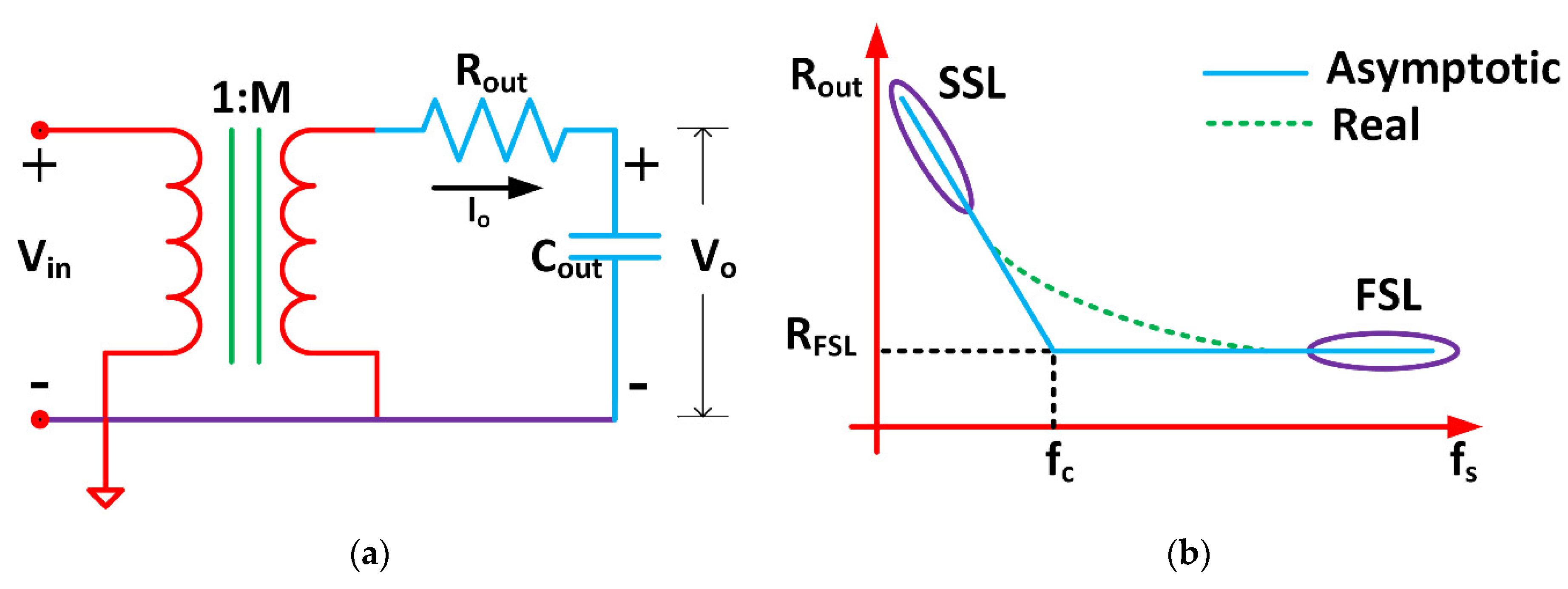
3. Integrated Switched Inductive Converters

For a wide range of voltage conversion ratios, inductive converters are promising candidates that deliver the best efficiency. Moreover, integrated inductive converters also provide higher efficiencies for a wide range of voltage conversion, along with high current densities. However, they depend on high-quality off-chip inductors [44].
The availability of integrated inductors that offer both low losses and high inductance density is due to recent developments. In order to provide the efficient on-chip power conversion at realistic current densities [45], planar spiral inductor topologies using a typical CMOS process have been built; these are popular in radio-frequency communication circuits [46]. Air-core inductors are relatively simple in structure and possess good integration possibilities [46,47]. For a 10 W output power, various air-core inductors are utilized in multi-phase Voltage-Controller Module utilities and achieves efficiencies in the range of 72% and 84% are accomplished for switching frequencies of 480 MHz and 100 MHz, respectively [47,48].The surface-mount technology (SMT)-based air-core inductors provide a current density of up to 1.7 A/mm2 [47,48,49]. However, the size and discrete nature of SMT components creates a difficulty in scaling. The integrated magnetic-core power inductors provide current densities as high as 8 A/mm2 and are highly scalable [50,51,52,53]. These inductors are useful in on-chip integration [15] and chip stacking [16].
Integrated inductive converters face the challenge of the requirement of high-quality inductors [47,48,49]. From the control viewpoint, inductive DC–DC converters allow good control of the output voltage for the variations in the input voltage and output load. Its output voltage is regulated by controlling the width of pulse that is fed to the power switches [54].
Inductive-switching power converters are highly suitable for off-chip applications, as they provide high power density, efficiency, and regulation. Inductive converters are commonly used for integration due to the ease of understanding of the fundamental operations of the circuit, control techniques, and availability of abundant number of topologies, and their capability for high power density and efficiency can be extended to ICs, even though challenges are experienced. The block diagram of the power stage of the synchronous inductive buck converter and corresponding steady-state waveforms are shown in Figure 5. Its derived topologies are well matched for fully monolithic integration. The important criterion is to check and neutralize the different power losses that restricts the 100% high efficiency for a switching power converter circuit.
The following section briefly discusses integrated inductive converters based on efficiency and power-loss contributions, control and modulation strategies, implementation issues, and integration technology options.

3.1. Power-Loss and Efficiency Calculations

The efficiency of an integrated inductive switching power converter (Ƞiisp) is defined as the ratio of output power to the input power, which is given as:
Ƞiisp = Po/Pin
where Pin = Po + Ploss, Po = the output power of the converter, Pin = the input power of the converter, and Ploss = the power loss in the converter.
The major losses are given below.

3.1.1. Conduction Losses

Ohmic losses in power switches and integrated inductor produces conduction losses, which are denoted as Pcond and are expressed as:
P c o n d = Σ i I 2 r m s , i R i
where Irms,i represents the rms value of current that is passing through ith resistor Ri. A small inductance is used in the integrated inductor due to technology restrictions, and this causes a large current ripple, followed by a large value of rms current. On the other hand, skin and proximity effects in the inductor windings cause the ohmic resistance to increase along with the increase in switching frequency. If the inductor is air-cored, the effective winding resistance of inductor further increases due to significant eddy current losses, which can significantly affect the converter’s efficiency [54].

3.1.2. Switching Losses

The charging and discharging of parasitic capacitances associated with Turn-On and Turn-Off causes the nonzero values of voltage and current. This leads to the switching losses Pswitch. To reduce the on-resistance of the power switches, Vdd is the maximum available voltage. In case of step-up, it is the output voltage Vo, and in case of step-down, it is Vin. In general, they are not straightforward to model and compute, but hold a proportional relationship to the switching frequency fs. These losses are given as:
P switch = Σ i f s C i V 2 dd
Gate driver losses, which can account for large portion of the switching losses can be limited either by using accurate dimensioning or using ascended voltage supplies.

3.1.3. Dead-Time Losses

When a switching converter is implemented as a synchronous rectifier, dead-time occurs. In CMOS processes, in the absence of fast-switching diodes, dead-time occurs during the OFF state of the power switches in order to avoid high current peaks. The dead-time losses are given as:
P dead = f s I L V diode t d
where IL represents the inductor current during the dead-time period, td represents dead-time, and Vdiode represents the forward bias voltage of the body diode. Dead-time losses are due to the current flowing through the body diode for every switching cycle, and they are considered as hybrid conduction/switching losses.

3.1.4. Inductor Core Losses

The magnetic core of an integrated inductor produces frequency dependent core losses, which includes hysteresis and eddy current losses [55]. The proper choice of core material reduces the EMI and the size of the inductor impression [49,56]. However, the pronounced core losses will occur, if the core material, thickness, and structure choice are not chosen carefully.

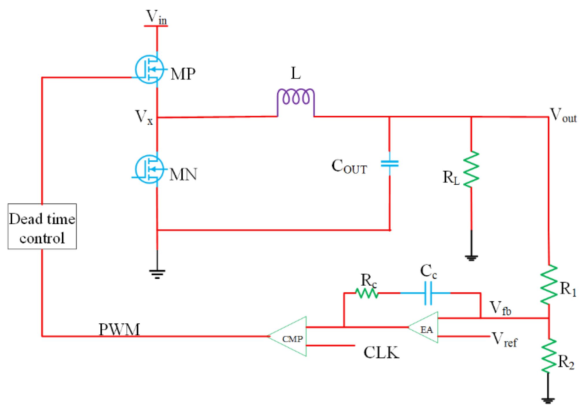
3.2. Control and Modulation Strategies

The controller is designed for a power converter to maintain the constant output voltage in the presence of input-voltage and load-current variations. The time constant associated with the high-frequency integrated power converters is very small, so additional care must be given in the process of designing a control loop [57]. The implementation of a control strategy requires modulation schemes that transform the control action into the switching pattern. The generated switching pattern decides the efficiency when the switching losses are significant.
Pulse-width modulation (PWM) and pulse-frequency modulation (PFM) [58] are pronounced modulation schemes in the case of high-frequency power converters. In the case of PWM, the switching frequency is kept fixed and the duty ratio is varied [59]. In PFM, the switching frequency is changed, and either constant ON time or constant OFF time is used to control the power switch. For low-power applications such as mobiles, PFM is a preferred choice over PWM when integrated inductive conversion is operated with a low switching frequency, which provides lower switching losses and a higher efficiency [57]. However, with PFM, the ripple in the output voltage is large at low power. However, this can be neutralized by placing a larger output capacitance that takes additional space. On the other hand, the advantage of PWM is better prediction of the EMI due to its constant switching frequency. When the switching frequency in PWM is high, there might be an interaction between the application’s frequency band and the EMI energy at the switching frequency, which is not desirable. To prevent this case, EMI energy is distributed across the frequency band for PFM-controlled integrated inductive power conversion circuits, and this becomes beneficial.

3.3. Implementation Issues

The boundary condition of integration requires the inductive converter topologies to choose the simple buck-and-boost topologies. For integrated inductive converters, isolated and resonant topologies are not suitable due to the requirements of an on-chip transformer and a low-quality factor, respectively [60]. In conventional buck-and-boost topologies, the measurement of on-state resistance of the switch and its related area, capacitance, and inductance are not straightforward. The primary consideration is given to the less-significant parasitic in the design of a conventional switch-mode power converter to provide the low-quality factor, followed by parasitic capacitances of a switch. To take these effects into account, the design equations need to be developed. The second critical aspects arise in formulation of the optimization problem in the multidimensional design space. Thus, the calculation of efficiency in the multidimensional design space over the entire design space based on the power-converter model becomes helpful [61,62,63].
For large Vdd and higher switching frequencies, decreasing the switching losses is most important (see Equation (8)). The charge and discharge of parasitic capacitances due to the flow of inductor current reduces the switching losses with zero-voltage switching (ZVS) in a quasi-resonant operation. Due to this, the energy is not dissipated in the switches; rather, it is swapped between the inductor and capacitor. The application of this idea to driver circuits results in the resonant gate drivers that operate at 200 MHz [64].
Another component to reduce the switching loss is associated with the dead-time of the body diode conduction. The inductor current raisess linearly when the upper PMOSFET is ON, and the same is discharged through the parasitic capacitance Cx at the node LX when the switch is OFF as shown in Figure 5. For appropriate control of the dead-time between the turn-on time instant of the lower NMOSFET and turn-off time instant of the upper PMOSFET, the NMOSFET can be turned ON when the voltage between the drain and source is zero. This discharges the parasitic capacitance Cx, and as a result, switching losses are reduced. In a similar way, the NMOSFET is turned OFF at the instant the inductor current becomes negative and it charges the CX [65], and the same is used in an integrated converter [66]. To arrest the turning ON of the MOSFET too early or too late, it becomes necessary that the dead-time needs to be controlled using adaptive control [67,68,69,70].
Multilevel power conversion using a conventional power converter was presented for integrated power conversion in [71] and recently extended in [72]. This decreases the value of RMS current and has more advantages in the form of reduced conduction losses, particularly in integrated inductive converters due to smaller inductance and related high current ripple, low Q-factor of the inductor, and related high series resistance. However, a major limitation in multilevel power conversion arises, as it requires a higher number of switches and associated gate driving signals when compared to the conventional topologies [71].
Multiphase power converters increase their maximum output power with the parallel connection of converter stages, since every stage contributes output power, and the same is limited for each stage. Furthermore, these converters can operate in such a way that all its stages operate at maximum possible efficiency, so that the overall converter efficiency improves. Based on the number of phases and the duty cycle, the complete output current ripple can be decreased significantly when the phases are out of phase. This implies the reduction of input and output capacitance related to a single converter with the same input and output ripples. On the other hand, the lower input and output voltage ripples will be the outcome with unchanged capacitance values. A two-phase integrated buck converter and four-phase integrated inductive buck converter can be found in [44,73]. Current ripple can be further decreased by coupling of inductors [74], which is not practicable when more than two phases are used.
The input voltage of the converter in many instances will be more than it can withstand in nm-CMOS IC processes. Cascaded connection of power switches using a regular CMOS allows tolerating high input or output voltages for both switched-inductive and capacitive converters [75]. Synthesizing high voltage (HV) MOSFETs in a baseline CMOS without the need of any extra process masks is another method [76]. These MOSFETS permit high switching-frequency operation, which is suitable in RF power amplifiers [77].
Another design parameter in integrated inductive converters is the requirement to operate in CCM or in DCM. In CCM, the inductor current does not approach zero, and provides satisfactory results due to ease of generation of switching signals. Its counterpart is DCM, in which the inductor current does not flow all the time; this is a viable option for low power when efficiency is more stringent [78]. Deciding whether to operate in CCM or in DCM is a primary choice, but to balance the losses for wide variation of output loads, or operate the converter with PFM [79] or in CCM/DCM, is to balance between the conduction and switching losses.

3.4. Integration Technology Options

Integration of converters majorly adopts SiP and monolithic integration techniques. Their details are as follows:
The reactive components in the SiP approach are executed in various technologies, leading to best implementation. The power IC was organized for a solenoid inductor by utilizing ferrite as substrate to arrange a chip-size module in [80]. On the other hand, using an off-chip surface mount device (SMD) and air-core capacitors and inductors, an eight-phase interleaved buck was designed in [47], an SC interleaved voltage doubler was designed in [81,82], and further to decrease the EMI, a single fully integrated cross-coupled SC voltage doublers is used [83].
In the dual-die approach, the reactive components are not kept on the same dies as the switches and its control. Here, the die with reactive elements and the active die are linked to each other through uneven patches. The reactive components with a characteristic size of 0.35 μm can be placed in a CMOS process in which the area is less costly, and then the active components can be added with load in nm CMOS [70]. A committed low-mask-count passive-integration process is beneficial to integrating inductors and capacitors to attain cost reduction. A passive-integration process of capacitance density with 80 nF/mm2 was used in [54,63] with a 8 μm-thick copper-top metal layer to synthesize inductors with a practical Q-factor. The large output and input capacitance values can be synthesized at low costs as an additional benefit.
Monolithically integrated inductive converters have been realized on a single die for an 130 nm CMOS [84] and 180 nm CMOS [85]. A buck converter was integrated monolithically on a 130 nm CMOS [86] and on a 180 nm SiGe IC [74], and recently via GaAs pHEMT [87]. Nevertheless, to integrate the inductor and attain a satisfactory performance in a basic CMOS is a challenging task in a selected area. Using bond wires, the inductors can be synthesized [88]. The postprocessing procedure can be applied to improve the performance of the inductor in a basic CMOS. To reduce EMI issues in a microelectromechanical system, a postprocessed plastic deformation magnetic assembly (PDMA) inductor was utilized due to the parallel connection between the magnetic fields and the planar circuits [46]. Based on an amorphous CoZrTa alloy, thin film inductors were suggested for the postprocessing procedure [89].

4. Comparison between Integrated SC and Inductive Converters

This section stipulates a comparative study of the SC and inductor-based converters in terms of the maximum efficiency versus power density of various appropriate designs; those discussed in the literature are depicted on a plane in Figure 6. Active and reactive dies were taken into account for calculating the total area and in turn the power density in SiP implementations. Some inferences regarding the suitability of the earlier discussed options are excluded from that assessment. From this evaluation, it can be pointed that the examples presented in the literature are not entirely comparable due to the involvement of various constraints and functionalities enforced by different applications (step-down, step-up, appropriate values of Vo and Vin). The considered performance metrics serve as the design guidelines in various applications.
Following are the noticeable points related to SCPCs (see Figure 6a):
(1)
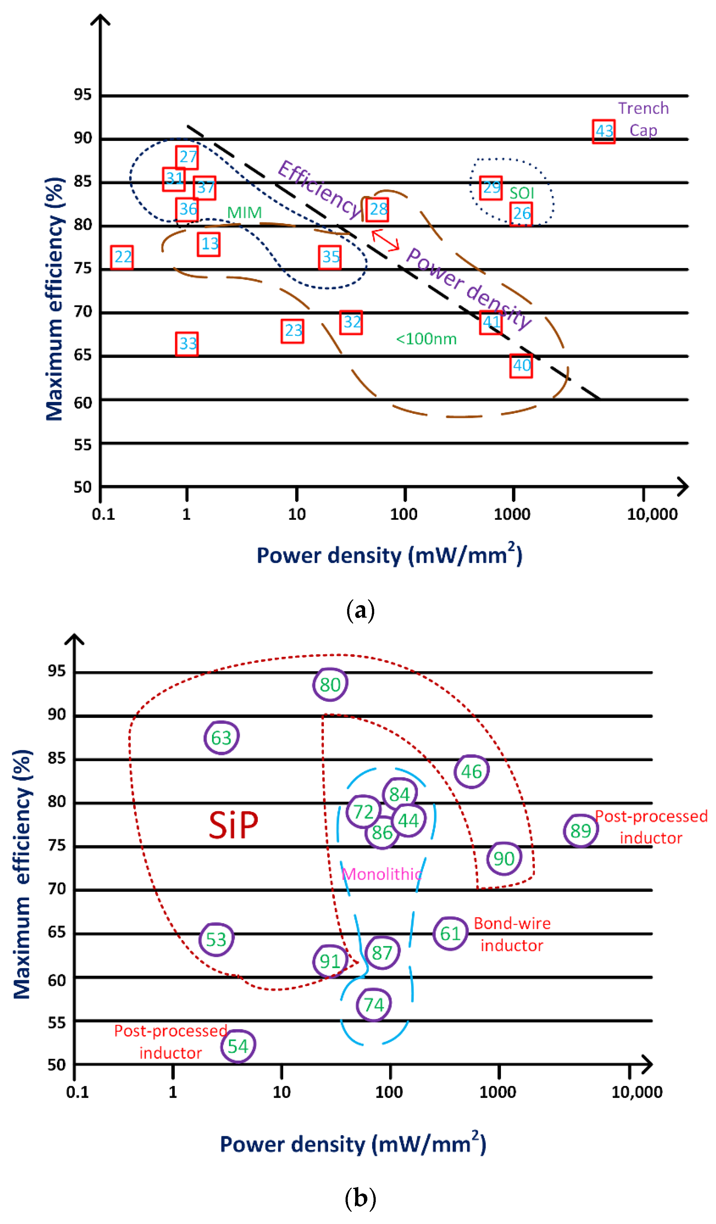
There is a comprehensible tradeoff between the maximum efficiency and the power density in bulk CMOS applications that include MIM capacitors. Using MIM capacitors allows higher peak efficiency designs, whereas lower capacitive density leads to lower power densities.
(2)
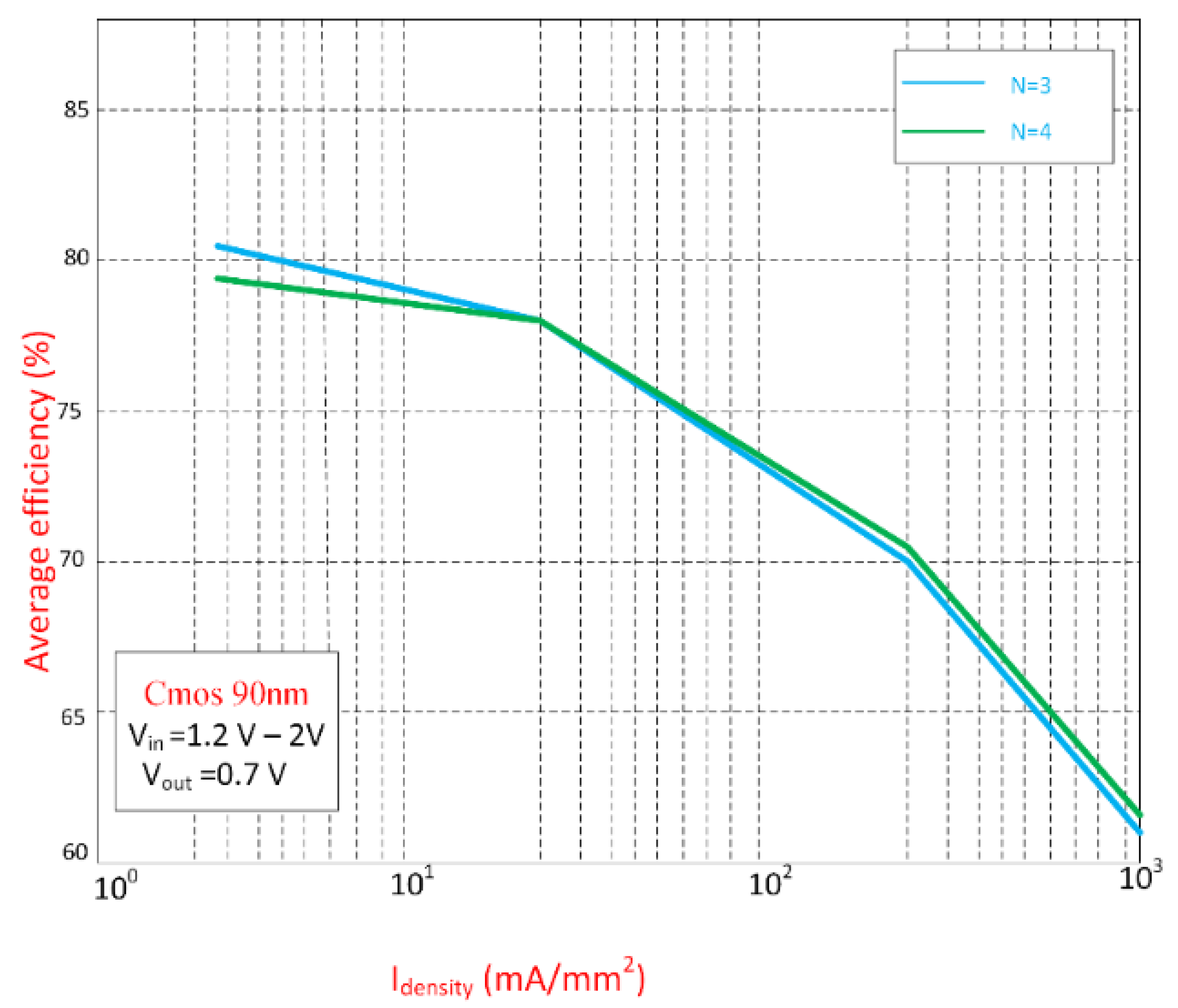
Operating the SCPC at higher switching frequencies results in a small size design, around 100 nm. This will give high power density at acceptable efficiencies for gate capacitance of MOS transistors.
(3)
Acceptable performance is acquired for different technologies as in [26] (fully integrated step-down SC converter), Ref. [29] (fully integrated step-down SC converter) and [43] (fully integrated SC 2:1 voltage converter), as shown in Figure 7 (trench capacitors).
(4)
It is challenging to determine the type of converter circuit (i.e., either SCPC or inductive converter) that can provide the satisfactory overall performance between the power density and the efficiency as depicted in Figure 6. The SCPC is the best possible design [43], but it engages at corresponding low voltage and affords low absolute output power. Therefore, it should be noted that the defined results strongly depend on application in relation to Po, Vo, Vin and other limitations.
Further, the following observations can be drawn regarding inductive converters (see Figure 6b):
(1)
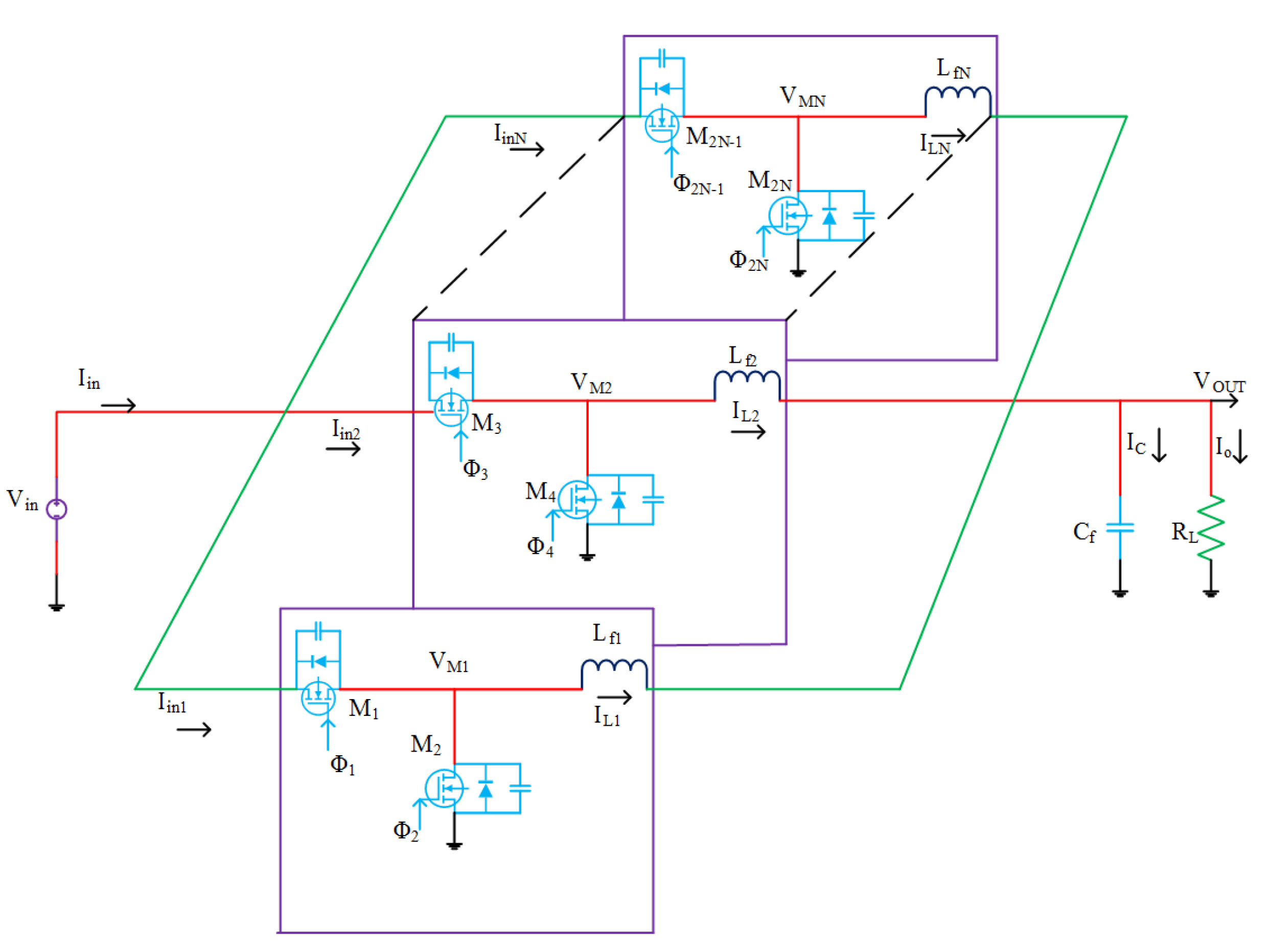
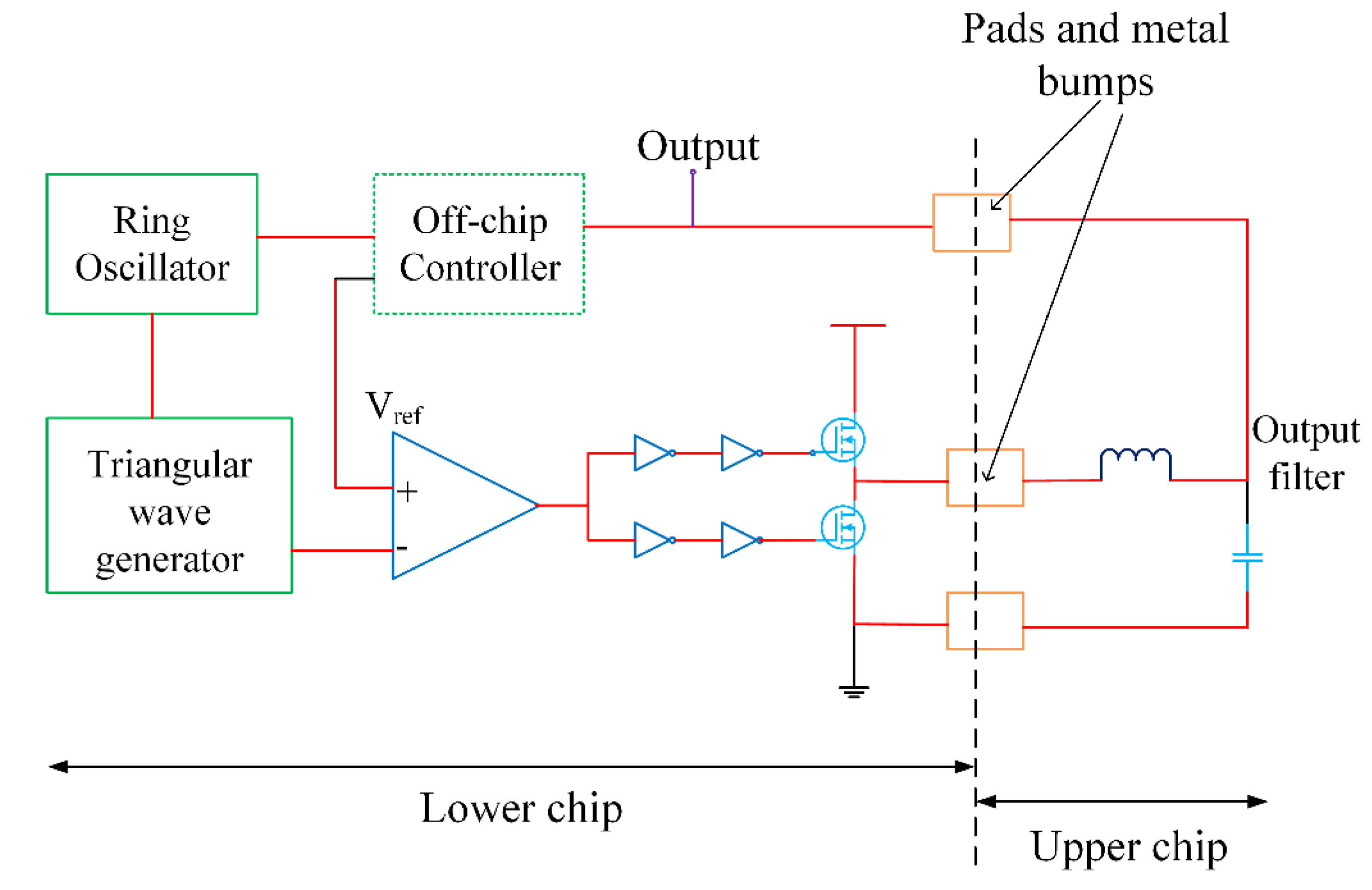
Without demanding special alterations, all the true monolithic converters realize comparable power densities [72] (fully integrated 3-level buck converter), as shown in Figure 8; Ref. [44] (fully integrated stacked interleaved buck converter), as shown in Figure 9; Ref. [74] (fully integrated four-phase step-down converter), as shown in Figure 10; Ref. [84] (fully integrated synchronous buck converter), as shown in Figure 11; Ref. [86] (fully integrated 3-level buck converter); and [87] (fully integrated multistage interleaved synchronous buck converter), as shown in Figure 12 (Ref. [87] is synthesized with SiGe rather than CMOS). Synthesizing the inductor using bond wires did not cause a large variation in the power density [88].
(2)
Compared to monolithic converters, SiP-based converters provide both higher [47] (integrated eight-phase synchronous buck converter), Ref. [90] (eight-phase integrated buck converter) and lower power densities [54] (integrated inductive step-down converter), Ref. [63] (integrated inductive step-down converter), Ref. [80] (integrated step-down converter), Ref. [91] (on-chip buck converter with stacked-chip implementation), as shown in Figure 13. The use of committed and advanced small SMD inductors and capacitors results in a higher power density [47]. So, the main motive for selecting SiP over the monolithic approach is the lower cost, but not the power density.
(3)
The power density of the converter can be improved after applying the postprocessing steps using the magnetic structures on CMOS [46] (integrated inductive step-down converter) [89]. Here, it is important to note that the choice of material plays a crucial role.
For off-chip applications, the reduced size and the copackage option of inductor-based switching converters are a step closer to complete integration [47]. However, they require costly fabrication steps [44] for improving the Q-factor of the inductor and a low energy density for fully integrated DC–DC converters based on CMOS inductors. Their counterpart, integrated capacitors, achieve low series resistance and high capacitance density. This allows them to be used for implementing DC–DC converters in CMOS processes without any extra construction stages. As a result, fully integrated SC converters are gaining interest in both academia and industrial researchers. Regarding SC converters [36,40], investigated the fully integrated SC with voltage doublers, using the interleaving of multiple phases to reduce the output ripple. The work in [36] demonstrated a high efficiency of 82% but a reduced power density of 0.67 mW/mm2, whereas the work in [40] achieved a high power density of 1.123 W/mm2 with a poor efficiency of 60%.
Using the works on DC–DC converters related to on-chip-integrated or package-integrated passive elements, Table 3 is presented to compare the test chips using different process technologies, input/output voltage ranges, inductor/capacitor technologies, power density, and efficiency.
It is difficult to make a fair comparison of the on-chip-integrated or the package-integrated technologies, as they differ in every aspect. However, Refs. [44,49,74] used the same technology with a power rating of more than 200 mW. So, only these works were considered for the comparison of the various parameters of DC–DC converters using the on-chip-integrated/package-integrated passive elements under the buck mode of operation [44,49,74]. The maximum output power and power density were chosen as the metrics for comparison, as they define the nature of application. It can be observed that [74] proposed buck operation for an output power of 0.8 W, which was two times more than the second highest value of 0.32 W, achieved in [44]. The designs in [49,74] share similar power densities of 0.213 W/mm2. However, Ref. [49] used off-chip air-core SMT inductors, which were not considered for the area calculation. In addition, it was found that when the process adopted SOI technology and implementation, using on-chip trench capacitor structures enabled higher efficiency.
Table 4 shows a comparison of step-up DC-DC converters with different viewpoints. It could be seen that the converters recorded in the table have on-chip capacitors, though the methods for realization of inductors are distinct. For instance [92] had utilized on-chip metal inductor and [93] had utilized bond wire to design the inductor. The data of power densities is given in Table 4. Commonly, power densities of the in-package inductor-based designs are considerably higher than those of the on-chip inductor-based designs. The proposed design in [94] depends on in- package inductor and it is noticed that the in-package inductor-based design has the best power density. The other significant perspective to notice here is that the decrease of output ripple. In [93] bond wires are utilized to realize the inductors, the ripple performance stays poor (around 6%), while in [94] in-package inductor is utilized and the ripple performance is 0.62%.
With a plethora of designs available in the literature pertaining to the choice of power converters, it was more challenging to find the suitability of a power converter for an application. This is shown in Figure 14 for both SCPCs and inductive converters based on the maximum output power obtained. Integrated inductive converters are more suitable for higher power levels [89,90]. Most of the designs, in the case of SCPCs, favored low-power applications. However, recently there were some investigations in [26,35] in 2010, and in [29,41] in 2011, to achieve the comparable output power levels as inductive converters.
Various SC voltage doublers are presented in Table 5. Fully integrated converters need using the bigger flying capacitors accessible in peripheral packages demanding higher switching frequencies. Parasitic losses of the coordinated CMOS capacitors decreases the highest reachable efficiency. Fully integrated designs grant the changes to work over a bigger operating region because of the essentially higher switching frequencies. From the Table 5, low EMI ([17,95]) is one of main advantage of the fully integrated converters compared to non- integrated converters ([83]). The improved EMI of fully integrated SC dc/dc converter empowers fully integrated power converters to be realized where the noise sensitivity confines their utilization.

5. Conclusions

This paper presented the technologies, modulation strategies, and control schemes of integrated switching power converters, both switched-capacitor and switched-inductive networks. Both types allow efficient conversion for up and down operations, which is essential in many applications. For the integrated switched-capacitor converters, a clear trade-off between peak efficiency and power density has been presented graphically to distinguish between MIM, SOI, and trench capacitor technologies. From the various control strategies of SCPCs, it was observed that the switching losses could be greatly reduced using the switching-frequency modulation technique, but at the same time, it enhanced the noise significantly. To overcome this problem, a capacitor-size modulation technique was used for reducing the effect of the switching frequency and noise to a great extent. For inductive converters, an SiP-based approach has both low and high power densities when compared to monolithic-approach-based converters due to the use of committed and advanced small SMD capacitors and inductors. It was also observed that the power density can be greatly increased by utilizing the postprocessed magnetic structures on a CMOS. Comparing the integrated versions of switched-capacitor and inductive converters, inductive converters are generally suited for higher output power applications. On the other side, integrated switched-capacitor converters are suitable for ultralow output powers.

Author Contributions

Conceptualization, G.K.K., T.K. and S.S.; methodology, T.K., D.E. and G.K.K.; writing—original draft preparation, T.K., G.K.K. and S.S.; investigation, F.B., S.S. and B.S.; resources, D.E. and B.S.; writing—review and editing, T.K., G.K.K. and S.S.; visualization, B.S. and D.E.; supervision, F.B. and S.S.; funding acquisition, F.B., and S.S. All authors have read and agreed to the published version of the manuscript.

Funding

This research received no external funding.

Institutional Review Board Statement

Not applicable.

Informed Consent Statement

Not applicable.

Data Availability Statement

Not applicable.

Conflicts of Interest

The authors declare no conflict of interest.

References

  1. Bergveld, H.J.; Kruijt, W.S.; Notten, P.H.L. Battery Management Systems: Design by Modelling. In Philips Research Book Series; Kluwer: Norwell, MA, USA, 2002; Volume 1. [Google Scholar]
  2. Lei, Y.; Liu, W.C.; Podgurski, R.C.N.P. An analytical method to evaluate and design hybrid switched-capacitor and multilevel converters. IEEE Trans. Power Electron. 2018, 33, 2227–2240. [Google Scholar] [CrossRef]
  3. Uno, M.; Sugiyama, K. Switched capacitor converter based multiport converter integrating bidirectional PWM and series-resonant converters for standalone photovoltaic systems. IEEE Trans. Power Electron. 2019, 34, 1394–1406. [Google Scholar] [CrossRef]
  4. Jiale, X.; Gu, L.; Rivas-Davila, J. Effect of Class 2 Ceramic Capacitor Variations on Switched-Capacitor and Resonant Switched-Capacitor Converters. IEEE J. Emerg. Sel. Top. Power Electron. 2020, 8, 2268–2275. [Google Scholar]
  5. Steyaert, M.; Tavernier, F.; Meyvaert, H.; Sarafianos, A.; Butzen, N. When Hardware Is Free, Power Is Expensive! Is Integrated Power Management the Solution? In Proceedings of the 41st European Solid-State Circuits Conference, Graz, Austria, 14–18 September 2015; pp. 26–34. [Google Scholar]
  6. Lu, Y.; Jiang, J.; Ki, W.-H.; Yue, C.P. A 123-Phase DC-DC Converter-Ring with Fast-DVS for Microprocessors. In Proceedings of the IEEE International Solid-State Circuits Conference (ISSCC), San Francisco, CA, USA, 22–26 February 2015; pp. 1–3. [Google Scholar]
  7. Karadi, R.; Piqué, G.V.; Bergveld, H.J. Switched-capacitor power converter topology overview and performance comparison. In Wideband Continuous-Time ∑ ∆ ADCs, Automotive Electronics, and Power Management; Springer: Cham, Switzerland, 2017; pp. 239–261. [Google Scholar]
  8. Lu, Y.; Jiang, J.; Ki, W.-H. Design considerations of distributed and centralized switched-capacitor converters for power supply on-chip. IEEE J. Emerg. Sel. Top. Power Electron. 2017, 6, 515–525. [Google Scholar] [CrossRef]
  9. Sanders, S.R.; Alon, E.; Le, H.P.; Seeman, M.D.; John, M.; Ng, V.W. The road to fully integrated DC–DC conversion via the switched-capacitor approach. IEEE Trans. Power Electron. 2012, 28, 4146–4155. [Google Scholar] [CrossRef]
  10. Meijer, M.; Liu, B.; van Veen, R.; de Gyvez, J.P. Post-Silicon Tuning Capabilities of 45nm Low-Power CMOS Digital Circuits. In Proceedings of the IEEE Symposium VLSI Circuits, Kyoto, Japan, 16–18 June 2009; pp. 110–111. [Google Scholar]
  11. Meijer, M.; de Gyvez, J.P.; Kapoor, A. Ultra-low-power digital design with body biasing for low area and performance-efficient operation. J. Low Power Electron. 2010, 6, 521–532. [Google Scholar] [CrossRef]
  12. Piqué, G.V.; Meijer, M. A 350nA Voltage Regulator for 90nm CMOS Digital Circuits with Reverse-Body-Bias. In Proceedings of the IEEE 37th Solid-State Circuits Conference, Helsinki, Finland, 12–16 September 2011; pp. 379–382. [Google Scholar]
  13. Kwong, J.; Ramadass, Y.K.; Verma, N.; Chandrakasan, A.P. A 65nm sub-Vt microcontroller with integrated SRAM and switched-capacitor DC-DC converter. IEEE J. Solid State Circuits 2009, 44, 115–126. [Google Scholar] [CrossRef] [Green Version]
  14. Van Breussegem, T.; Wens, M.; Redouté, J.-M.; Geukens, E.; Geys, D.; Steyaert, M. A DMOS Integrated 320mW Capacitive 12V to 70V DC/DC Converter for LIDAR Applications. In Proceedings of the 2009 Energy Conversion Congress and Exposition, San Jose, CA, USA, 20–24 September 2009; pp. 3865–3869. [Google Scholar]
  15. Ebrahim, M.A.; Abdel Fattah, R.M.; Saied, E.M.; Abdel Maksoud, S.M.; El Khash, H. Droop Control of an Islanded Microgrid Using Harris Hawks Optimization Algorithm. Int J. Appl. Math. Comput. Sci. Syst. Eng. 2021, 3, 48–53. [Google Scholar]
  16. El-Bayeh, C.Z. A Review on Charging Strategies of Plug-in Electric Vehicles. Eng. World 2019, 1, 9–33. [Google Scholar]
  17. Wittmann, J.; Neidhardt, J.; Wicht, B. EMC optimized design of linear regulators including a charge pump. IEEE Trans. Power Electron. 2013, 28, 4594–4602. [Google Scholar] [CrossRef]
  18. Khan, M.N.H.; Forouzesh, M.; Siwakoti, Y.P.; Li, L.; Blaabjerg, F. Switched capacitor integrated (2n + 1)-level step-up single-phase inverter. IEEE Trans. Power Electron. 2019, 35, 8248–8260. [Google Scholar] [CrossRef]
  19. Arntzen, B.; Maksimovic, D. Switched-capacitor DC/DC converters with resonant gate drive. IEEE Trans. Power Electron. 1998, 13, 892–902. [Google Scholar] [CrossRef] [Green Version]
  20. Seeman, M.D.; Sanders, S.R. Analysis and optimization of switched capacitor DC–DC converters. IEEE Trans. Power Electron. 2008, 23, 841–851. [Google Scholar] [CrossRef]
  21. Makowski, M.; Maksimovic, D. Performance Limits of Switched Capacitor DC–DC Converters. In Proceedings of the IEEE Power Electronics Specialists Conference, Atlanta, GA, USA, 18–22 June 1995; pp. 1215–1221. [Google Scholar]
  22. Ramadass, Y.K.; Chandrakasan, A.P. Voltage Scalable Switched Capacitor DC–DC Converter for Ultra-Low Power On-Chip Applications. In Proceedings of the IEEE Power Electronics Specialists Conference, Orlando, FL, USA, 17–21 June 2007; pp. 2353–2359. [Google Scholar]
  23. Maksimovic, D.; Dhar, S. Switched-Capacitor DC-DC Converters for Low-Power On-Chip Applications. In Proceedings of the IEEE Power Electronics Specialists Conference, Charleston, SC, USA, 1 July 1999; pp. 54–59. [Google Scholar]
  24. Villar, G.; Alarcon, E.; Madrenas, J.; Guinjoan, F.; Poveda, A. Energy Optimization of Tapered Buffers for CMOS On-Chip Switching Power Converters. In Proceedings of the IEEE International Symposium Circuits System, Piscataway, NJ, USA, 23–26 May 2005; pp. 4453–4456. [Google Scholar]
  25. Villar-Pique, G.; Bergveld, H.J.; Alarcon, E. Survey and benchmark of fully integrated switching power converters: Switched-capacitor versus inductive approach. IEEE Trans. Power Electron. 2013, 28, 4156–4167. [Google Scholar] [CrossRef] [Green Version]
  26. Le, H.P.; Seeman, M.; Sanders, S.R.; Sathe, V.; Naffziger, S.; Alon, E. A 32nm Fully Integrated Reconfigurable Switched-Capacitor DC-DC Converter Delivering 0.55w/mm2 at 81% Efficiency. In Proceedings of the IEEE International Solid-State Circuit Conference, San Francisco, CA, USA, 7–11 February 2010; pp. 210–211. [Google Scholar]
  27. Van Breussegem, T.; Steyaert, M. A Fully Integrated Gearbox Capacitive DC/DC-Converter in 90nm CMOS: Optimization, Control and Measurements. In Proceedings of the IEEE Workshop Control Modeling Power Electronics, Boulder, CO, USA, 28–30 June 2010; pp. 1–5. [Google Scholar]
  28. Villar Piqué, G. A 41-Phase Switched-Capacitor Power Converter with 3.8 mv Output Ripple and 81% Efficiency in Baseline 90 nm CMOS. In Proceedings of the IEEE International Solid-State Circuit Conference, San Francisco, CA, USA, 19–23 February 2012; pp. 98–100. [Google Scholar]
  29. Le, H.P.; Sanders, S.R.; Alon, E. Design techniques for fully integrated switched-capacitor DC-DC converters. IEEE J. Solid State Circuits 2011, 46, 2120–2131. [Google Scholar] [CrossRef]
  30. Bin, S.; Yujia, Y.; Ying, W.; Zhiliang, H. High Efficiency, Inductor Less Step-Down DC/DC Converter. In Proceedings of the IEEE International Conference ASIC, Shanghai, China, 24–27 October 2005; pp. 364–367. [Google Scholar]
  31. Rao, A.; McIntyre, W.; Moon, U.K.; Temes, G.C. Noise-shaping techniques applied to switched-capacitor voltage regulators. IEEE J. Solid State Circuits 2005, 40, 422–429. [Google Scholar] [CrossRef]
  32. Ramadass, Y.K.; Fayed, A.A.; Chandrakasan, A.P. A fully-integrated switched-capacitor step-down DC-DC converter with digital capacitance modulation in 45 nm CMOS. J. Solid State Circuits 2010, 45, 2557–2565. [Google Scholar] [CrossRef]
  33. Ling, S.; Dongsheng, M.; Brokaw, A.P. A Monolithic Step-down SC Power Converter with Frequency-Programmable Sub-threshold Z-Domain Dpwm Control for UL-Tra-Low Power Microsystems. In Proceedings of the IEEE European Solid-State Circuit Conference, Edinburgh, UK, 15–19 September 2008; pp. 56–61. [Google Scholar]
  34. Ling, S.; Dongsheng, M.; Brokaw, A.P. Design and analysis of monolithic step-down SC power converter with sub-threshold DPWM control for self-powered wireless sensors. IEEE Trans. Circuits Syst. I Regul. Pap. 2010, 57, 280–290. [Google Scholar] [CrossRef]
  35. Van Breussegem, T.; Steyaert, M. A Fully Integrated 74% Efficiency 3.6v to 1.5v 150mw Capacitive Point of Load DC/DC Converter. In Proceedings of the IEEE European Solid-State Circuit Conference, Seville, Spain, 13–17 September 2010; pp. 434–437. [Google Scholar]
  36. Van Breussegem, T.; Steyaert, M. A 82% Efficiency 0.5% Ripple 16-Phase Fully Integrated Capacitive Voltage Doubler. In Proceedings of the IEEE Symposium VLSI Circuits, Kyoto, Japan, 16–18 June 2009; pp. 198–199. [Google Scholar]
  37. Seeman, M.D.; Sanders, S.R.; Rabaey, J.M. An Ultra-Low-Power Power Management IC for Energy-Scavenged Wireless Sensor Nodes. In Proceedings of the IEEE Power Electronics Specialists Conference, Rhodes, Greece, 15–19 June 2008; pp. 925–931. [Google Scholar]
  38. Bhattacharyya, K.; Kumar, P.V.R.; Mandal, P. Embedded Hybrid DC-DC Converter with Improved Power Efficiency. In Proceedings of the IEEE International Midwest Symposium Circuits System, Cancun, Mexico, 2–5 August 2009; pp. 945–948. [Google Scholar]
  39. Wieckowski, M.; Chen, G.K.; Seok, M.; Blaauw, D.; Sylvester, D. A Hybrid DC-DC Converter for Sub-Microwatt Sub-1V Implantable Applications. In Proceedings of the IEEE Symposium VLSI Circuits, Kyoto, Japan, 16–18 June 2009; pp. 166–167. [Google Scholar]
  40. Somasekhar, D.; Srinivasan, B.; Pandya, G.; Hamzaoglu, F.; Khellah, M.; Karnik, T.; Zhang, K. Multi-phase 1GHz voltage doubler charge pump in 32nm logic process. IEEE J. Solid State Circuits 2010, 45, 751–758. [Google Scholar] [CrossRef]
  41. Meyvaert, H.; van Breussegem, T.; Steyaert, M. A Monolithic 0.77w/mm2 Power Dense Capacitive DC-DC Step-Down Converter in 90nm Bulk CMO. In Proceedings of the IEEE 37th Solid-State Circuits Conference, Helsinki, Finland, 12–16 September 2011; pp. 483–486. [Google Scholar]
  42. Klootwijk, J.H.; Jinesh, K.B.; Dekkers, W.; Verhoeven, J.F.; van den Heuvel, F.C.; Kim, H.D.; Blin, D.; Verheijen, M.A.; Weemaes, R.; Kaiser, M. Ultrahigh capacitance density for multiple ALD-grown MIM capacitor stacks in 3-D silicon. IEEE Electron Device Lett. 2008, 29, 740–742. [Google Scholar] [CrossRef]
  43. Leland, C.; Montoye, R.K.; Ji, B.L.; Weger, A.J.; Stawiasz, K.G.; Dennard, R.H. A Fully-Integrated Switched-Capacitor 2:1 Voltage Converter with Regulation Capability and 90% Efficiency at 2.3a/mm2. In Proceedings of the IEEE Symposium VLSI Circuits, Honolulu, HI, USA, 15–17 June 2010; pp. 55–56. [Google Scholar]
  44. Wibben, J.; Harjani, R. A high-efficiency DC-DC converter using 2 nH integrated inductors. J. Solid State Circuits 2008, 43, 844–854. [Google Scholar] [CrossRef]
  45. Wibben, J.; Harjani, R. A High Efficiency DC-DC Converter Using 2 nH On-Chip Inductors. In Proceedings of the 2007 IEEE Symposium VLSI Circuits, Kyoto, Japan, 14–16 June 2007; pp. 22–23. [Google Scholar]
  46. Musunuri, S.; Chapman, P. Design of Low Power Monolithic DC-DC Buck Converter with Integrated Inductor. In Proceedings of the IEEE Power Electronics Specialists Conference, Dresden, Germany, 16 June 2005; pp. 1773–1779. [Google Scholar]
  47. Schrom, G.; Hazucha, P.; Paillet, F.; Rennie, D.J.; Moon, S.T.; Gardner, D.S.; Kamik, T.; Sun, P.; Nguyen, T.T.; Hill, M.J. A 100 mhz Eight-Phase Buck Converter Delivering 12 a in 25 mm2 Using Air-Core Inductors. In Proceedings of the IEEE Applied Power Electronics Conference, Anaheim, CA, USA, 25 February–1 March 2007; pp. 727–730. [Google Scholar]
  48. Schrom, G.; Hazucha, P.; Hahn, J.; Gardner, D.; Bloechel, B.; Dermer, G.; Narendra, S.; Karnik, T.; De, V. A 480-MHz, Multi-Phase Interleaved Buck DC-DC Converter with Hysteretic Control. In Proceedings of the IEEE Power Electronics Specialists Conference, PESC’04, Piscataway, NJ, USA, 20–25 June 2004; Volume 6, pp. 4702–4707. [Google Scholar]
  49. Hazucha, P.; Schrom, G.; Hahn, J.; Bloechel, B.A.; Hack, P.; Dermer, G.E.; Narendra, S.; Gardner, D.; Karnik, T.; De, V. A 233 MHz 80%–87% efficient four-phase DC-DC converter utilizing air-core inductors on package. J. Solid State Circuits 2005, 40, 838–845. [Google Scholar] [CrossRef]
  50. Gardner, D.S.; Schrom, G.; Paillet, F.; Jamieson, B.; Karnik, T.; Borkar, S. Review of on-chip inductor structures with magnetic films. IEEE Trans. Magn. 2009, 45, 4760–4766. [Google Scholar] [CrossRef]
  51. Morrow, P.R.; Park, C.M.; Koertzen, H.W.; Dibene, J.T. Design and fabrication of on-chip coupled inductors integrated with magnetic material for voltage regulators. IEEE Trans. Magn. 2011, 47, 1678–1686. [Google Scholar] [CrossRef]
  52. Sturcken, N.; Davies, R.; Cheng, C.; Baileys, W.E.; Shepard, K.L. Design of Coupled Power Inductors with Crossed Anisotropy Magnetic Core for Integrated Power Conversion. In Proceedings of the 27th Annual IEEE Applied Power Electronics Conference Exposition, APEC 2012, Orlando, FL, USA, 5–9 February 2012; pp. 417–423. [Google Scholar]
  53. Sturcken, N.; Petracca, M.; Warren, S.; Mantovani, P.; Carloni, L.P.; Peterchev, A.V.; Shepard, K.L. A switched-inductor integrated voltage regulator with nonlinear feedback and network-on-chip load in 45 nm SOI. J. Solid State Circuits 2012, 47, 1935–1945. [Google Scholar] [CrossRef] [Green Version]
  54. Bergveld, H.J.; Karadi, R.; Nowak, K. An Inductive Down Converter System-in-Package for Integrated Power Management in Battery-Powered Applications. In Proceedings of the IEEE Power Electronics Specialists Conference, Rhodes, Greece, 15–19 June 2008; pp. 3335–3341. [Google Scholar]
  55. Meere, R.; O’Donnell, T.; Bergveld, H.J.; Ningning, W.; O’Mathuna, S.C. Analysis of micro inductor performance in a 20-100 MHz DC/DC converter. IEEE Trans. Power Electron. 2009, 24, 2212–2218. [Google Scholar] [CrossRef] [Green Version]
  56. Schrom, G.; Faillet, F.; Hahn, J. A 60 Mhz 50wfine-Grain Package Integrated vr Powering a CPU from 3.3 V. In Proceedings of the Applied Power Electronics Conference, Palm Springs, CA, USA, 21–25 February 2010. [Google Scholar]
  57. Wens, M. Monolithic Inductive CMOS DC-DC Converters—Theory Study and Implementation. Ph.D. Thesis, Dep. Elektrotechniek, Katholieke Universiteit Leuven, Leuven, Belgium, October 2010. [Google Scholar]
  58. Erickson, R.W.; Maksimovic, D. Fundamentals of Power Electronics, 2nd ed.; Springer: New York, NY, USA, 2001. [Google Scholar]
  59. Akroum, H.; Kidouche, M.; Aibeche, A. Scalar Control of Induction Motor Drives Using dSPACE DS1104. In Proceedings of the International Conference on Systems, Control and Informatics, 28 September 2013; pp. 322–327. [Google Scholar]
  60. Deleage, O.; Crebier, J.C.; Brunet, M.; Lembeye, Y.; Manh, H.T. Design and realization of highly integrated isolated DC/DC microconverter. IEEE Trans. Ind. Appl. 2011, 47, 930–938. [Google Scholar] [CrossRef]
  61. Haizoune, F.; Bergveld, H.J.; Popovic-Gerber, J.; Ferreira, J.A. Topology Comparison and Design Optimisation of the Buck Converter and the Single-Inductor Dual-Output Converter for Sys-Tem-in-Package in 65 nm CMOS. In Proceedings of the IEEE International Power Electronic Motion Control Conference, Piscataway, NJ, USA, 17–20 May 2009; pp. 295–301. [Google Scholar]
  62. Piqué, G.V.; Alarcón, E. CMOS Integrated Switching Power Converters: A Structured Design Approach, 1st ed.; Springer: Berlin, Germany, 2011. [Google Scholar]
  63. Bergveld, H.J.; Nowak, K.; Karadi, R.; Iochem, S.; Ferreira, J.; Ledain, S.; Pieraerts, E.; Pommier, M. A 65-NM CMOS 100-Mhz 87%-Efficient DC-DC Down Converter Based on Dual-Die System-in-Package Integration. In Proceedings of the IEEE Energy Conversion Congress Exposition, San Jose, CA, USA, 20–24 September 2009; pp. 3698–3705. [Google Scholar]
  64. Bathily, M.; Allard, B.; Hasbani, F. A 200-MHz integrated buck converter with resonant gate drivers for an RF power amplifier. IEEE Trans. Power Electron. 2012, 27, 610–613. [Google Scholar] [CrossRef]
  65. Maksimovic, D. Design of the Zero-Voltage-Switching Quasi-Square-Wave Resonant Switch. In Proceedings of the IEEE Power Electronics Specialists Conference, Seattle, WA, USA, 20–24 June 1993; pp. 323–329. [Google Scholar]
  66. Trescases, O.; Ng, W.T. Variable Output, Soft-Switching DC/DC Converter for Vlsi Dynamic Voltage Scaling Power Supply Applications. In Proceedings of the IEEE 35th Annual Power Electronics Specialists Conference, Aachen, Germany, 20–25 June 2004; Volume 6, pp. 4149–4155. [Google Scholar]
  67. Lau, W.; Sanders, S. An Integrated Controller for a High-Frequency Buck Converter. In Proceedings of the IEEE Power Electronics Specialists Conference, Saint Louis, MO, USA, 27 June 1997; pp. 246–254. [Google Scholar]
  68. Chen, S.; Trescases, O.; Ng, W.T. Fast Dead-Time Locked Loops for a High-Efficiency Microprocessor-Load Zvs-Qsw DC/DC Converter. In Proceedings of the IEEE Conference on Electron Devices and Solid-State Circuits, Hong Kong, China, 16–18 December 2003; pp. 391–394. [Google Scholar]
  69. Trescases, O.; Ng, W.T.; Chen, S. Precision Gate Drive Timing in a Zero-Voltage-Switching DC-DC Converter. In Proceedings of the IEEE Symposium Power Semiconductor Devices ICs, Kitakyushu, Japan, 17–24 May 2004; pp. 55–58. [Google Scholar]
  70. Maderbacher, G.; Jackum, T.; Pribyl, W.; Wassermann, M.; Petschar, A.; Sandner, C. Automatic Dead Time Optimization in a High Frequency Dcdc Buck Converter in 65 NM CMOS. In Proceedings of the European Solid-State Circuits Conference, Helsinki, Finland, 12–16 September 2011; pp. 487–490. [Google Scholar]
  71. Piqué, G.V.; Alarcon, E. Monolithic Integration of a 3-Level Dcmoperated Low-Floating-Capacitor Buck Converter Fordc-DC Step-down Conversion in Standard CMOS. In Proceedings of the IEEE Power Electronics Specialists Conference, Rhodes, Greece, 15–19 June 2008; pp. 4229–4235. [Google Scholar]
  72. Kim, W.; Brooks, D.; Wei, G.-Y. A fully-integrated 3-level DC-DC converter for nanosecond-scale DVFS. IEEE J. Solid State Circuits 2012, 47, 206–219. [Google Scholar] [CrossRef]
  73. Wens, M.; Steyaert, M. An 800 MW Fully Integrated 130nm CMOS DC-DC Step-down Multi-Phase Converter with on-Chip Spiral Inductors and CA-Pacitors. In Proceedings of the IEEE Energy Conversion Congress Exposition, San Jose, CA, USA, 20–24 September 2009; pp. 3706–3709. [Google Scholar]
  74. Schrom, G.; Hazucha, P.; Hahn, J.H.; Kursun, V.; Gardner, D.; Narendra, S.; Karnik, T.; De, V. Feasibility of Monolithic and 3d-Stacked DC-DC Converters for Microprocessors in 90nm Technology Generation. In Proceedings of the IEEE International Symposium of Low-Power Electronics and Design, Newport Beach, CA, USA, 5 August 2004; pp. 263–268. [Google Scholar]
  75. Kursun, V.; Narendra, S.G.; De, V.K.; Friedman, E.G. High Input Voltage Step-down DC-DC Converters for Integration in a Low Voltage CMOS Process. In Proceedings of the IEEE International Symposium Quality Electronic Design, San Jose, CA, USA, 22–24 March 2004; pp. 517–521. [Google Scholar]
  76. Heringa, A.; Sonsky, J. Novel Power Transistor Design for a Process Independent High Voltage Option in Standard CMOS. In Proceedings of the IEEE Symposium Power Semiconductor Devices IC’s, Naples, Italy, 4–8 June 2006; pp. 1–4. [Google Scholar]
  77. Calvillo-Cortes, D.A.; Acar, M.; van der Heijden, M.P.; Apostolidou, M.; de Vreede, L.C.N.; Leenaerts, D.; Sonsky, J. A 65 nm Pulse-Widthcontrolled Driver with 8Vpp Output Voltage for Switched-Mode RF Pas up to 3.6ghz. In Proceedings of the IEEE International Solid-State Circuits Conference, San Francisco, CA, USA, 20–24 February 2011; pp. 12–14. [Google Scholar]
  78. Peng, H.; Wright, P.; Hella, M.M.; Chow, T.P. Integrated high frequency power converters based on GaAs pHEMT: Technology characterization and design examples. IEEE Trans. Power Electron. 2012, 27, 2644–2656. [Google Scholar]
  79. Li, P.; Bhatia, D.; Xue, L.; Bashirullah, R. A 90–240 MHz hysteretic controlled DC-DC buck converter with digital phase locked loop synchronization. J. Solid State Circuits 2011, 46, 2108–2119. [Google Scholar] [CrossRef]
  80. Hayashi, Z.; Katayama, Y.; Edo, M.; Nishio, H. High-efficiency DCDC converter chip size module with integrated soft ferrite. IEEE Trans. Magn. 2003, 39, 3068–3072. [Google Scholar] [CrossRef]
  81. Su, F.; Ki, W.; Tsui, C. Regulated switched-capacitor doubler with interleaving control for continuous output regulation. J. Solid State Circuits 2009, 44, 1112–1120. [Google Scholar] [CrossRef]
  82. Xiaojian, Y.; Moez, K.; Wey, I.-C.; Sawan, M.; Chen, J. A fully integrated multistage cross-coupled voltage multiplier with no reversion power loss in a standard CMOS process. IEEE Trans. Circuits Syst. II Express Briefs 2016, 64, 737–741. [Google Scholar]
  83. Lee, H.; Mok, P. Switching noise and shoot-through current reduction techniques for switched-capacitor voltage doubler. J. Solid State Circuits 2005, 40, 1136–1146. [Google Scholar] [CrossRef] [Green Version]
  84. Jinhua, N.; Hong, Z.; Liu, B.Y. Improved On-Chip Components for Integrated DC-DC Converters in 0.13 μm CMOS. In Proceedings of the IEEE European Solid-State Circuits Conference, Athens, Greece, 14–18 September 2009; pp. 448–451. [Google Scholar]
  85. Alimadadi, M.; Sheikhaei, S.; Lemieux, G.; Mirabbasi, S.; Dunford, W.G.; Palmer, P.R. A fully integrated 660 MHz low-swing energy-recycling DC-DC converter. IEEE Trans. Power Electron. 2009, 24, 1475–1485. [Google Scholar] [CrossRef]
  86. Kudva, S.S.; Harjani, R. Fully-integrated on-chip DC-DC converter with a 450× output range. J. Solid State Circuits 2011, 46, 1940–1951. [Google Scholar] [CrossRef]
  87. Abedinpour, S.; Bakkaloglu, B.; Kiaei, S. A multistage interleaved synchronous buck converter with integrated output filter in 0.18μm SiGe process. IEEE Trans. Power Electron. 2007, 22, 2164–2175. [Google Scholar] [CrossRef]
  88. Wens, M.; Steyaert, M. A Fully Integrated 0.18 μM CMOS DC-DC Step-down Converter, Using a Bondwire Spiral Inductor. In Proceedings of the IEEE Custom Integrated Circuits Conference, San Jose, CA, USA, 21–14 September 2008; pp. 17–20. [Google Scholar]
  89. DibeneII, J.T. Power on Silicon with on-Die Magnetics—the Start of a Revolution in Power Delivery and Power Management for Soc’s and High-Performance Applications. In Proceedings of the 2nd International Workshop Power Supply Chip, Cork, Ireland, 13 October 2010. [Google Scholar]
  90. Sturcken, N.; O’Sullivan, E.J.; Wang, N.; Herget, P.; Webb, B.; Romankiw, L.T.; Petracca, M.; Davies, R.; Fontana, R.; Decad, G.M.; et al. A 2.5d Integrated Voltage Regulator Using Coupled Magnetic-Core Inductors on Silicon Interposer Delivering 10.8a/mm2. In Proceedings of the IEEE International Solid-State Circuit Conference, San Francisco, CA, USA, 19–23 February 2012. Session 23. [Google Scholar]
  91. Onizuka, K.; Inagaki, K.; Kawaguchi, H.; Takamiya, M.; Sakurai, T. Stacked-chip implementation of on-chip buck converter for distributed power supply system in SiPs. J. Solid State Circuits 2007, 42, 2404–2410. [Google Scholar] [CrossRef]
  92. Hernandez, H.; Kofuji, S.T.; van Noije, W. Fully Integrated Boost Converter for Thermoelectric Energy Harvesting. In Proceedings of the 2013 IEEE 4th Latin American Symposium on Circuits and Systems (LASCAS), Cusco, Peru, 27 February–1 March 2013. [Google Scholar]
  93. Wens, M.; Steyaert, M. A Fully-Integrated 0.18 μm CMOS DC-DC Step-Up Converter, Using a Bondwire Spiral Inductor. In Proceedings of the 33rd European Solid State Circuits Conference, Muenchen, Germany, 11–13 September 2007; pp. 268–271. [Google Scholar]
  94. Dam, S.; Mandal, P. An integrated DC–DC boost converter having low-output ripple suitable for analog applications. IEEE Trans. Power Electron. 2017, 33, 5108–5117. [Google Scholar] [CrossRef]
  95. Kennedy, S.; Yuce, M.R.; Redouté, J.-M. A Low-EMI Fully Integrated Switched-Capacitor DC/DC Converter. IEEE Trans. Electromagn. Compat. 2017, 60, 225–233. [Google Scholar] [CrossRef]
Figure 1. SC converter model and its equivalent output resistance VS frequency: (a) SC converter average model [19]; (b) output resistance of an SCPC (Switched Capacitor Power Converter) as a function of the switching frequency fs [20]. Reproduced from [19], IEEE TRANSACTIONS ON POWER ELECTRONICS: 1998 [20], IEEE TRANSACTIONS ON POWER ELECTRONICS: 2008.
Energies 14 03250 g001
Figure 2. Example of two circuit topologies of SCPCs with M = 0.25 exhibiting different output impedances with three floating capacitors [21]. Reproduced from [21], In Proceedings of the IEEE Power Electronics Specialists Conference: 1995.
Energies 14 03250 g002
Figure 3. Comparison of a multiratio switched-capacitor converter’s theoretical efficiency (without including switching losses), with N = 2, 3, 4. ‘N’ represents the number of capacitors together with the output capacitor Cout [25]. Reproduced from [25], IEEE TRANSACTIONS ON POWER ELECTRONICS:2013.
Energies 14 03250 g003
Figure 4. Efficiency comparison of two different MR-SCPCs, with N = 3 and N = 4, as a function of the current density by considering switching losses [28]. Reproduced from [28], In Proceedings of the IEEE International Solid-State Circuit Conference: 2012.
Energies 14 03250 g004
Figure 5. Block diagram of the power stage of the synchronous inductive buck converter with corresponding steady-state waveforms [54]. Reproduced from [54], In Proceedings of the IEEE Power Electronics Specialists Conference: 2008.
Energies 14 03250 g005
Figure 6. Comparison of maximum efficiency versus power density of various designs discussed in the literature for (a) switched-capacitor and (b) inductive converters [28]. Reproduced from [28] In Proceedings of the IEEE International Solid-State Circuit Conference: 2012.
Energies 14 03250 g006
Figure 7. A 2:1 step-down SC DC–DC converter [43]. Reproduced from [43], In Proceedings of the IEEE Symposium VLSI Circuits: 2010.
Energies 14 03250 g007
Figure 8. Schematic of the 3-level power converter [72]. Reproduced from [72], IEEE Journal of Solid State Circuits: 2012.
Energies 14 03250 g008
Figure 9. Stacked interleaved topology [44]. Reproduced from [44], IEEE Journal of Solid State Circuits: 2008.
Energies 14 03250 g009
Figure 10. A four-phase buck converter [73]. Reproduced from [73], In Proceedings of the IEEE Energy Conversion Congress Exposition: 2009.
Energies 14 03250 g010
Figure 11. Synchronous buck converter and its control [84]. Reproduced from [84], In Proceedings of the IEEE European Solid-State Circuits Conference: 2009.
Energies 14 03250 g011
Figure 12. Circuit diagram of multistage interleaved synchronous DC–DC buck converters [87]. Reproduced from [87], IEEE Transactions on Power Electronics: 2007.
Energies 14 03250 g012
Figure 13. Test circuit diagram of stacked-chip implementation of a buck converter [91]. Reproduced from [91], IEEE Journal of Solid State Circuits: 2007.
Energies 14 03250 g013
Figure 14. Maximum output power vs. peak efficiency of different designs in the literature for inductive and switched-capacitor converters.
Energies 14 03250 g014
Table 1. Number of floating capacitors (N − 1) VS feasible conversion ratios (m) [21]. Reproduced from [21], In Proceedings of the IEEE Power Electronics Specialists Conference: 1995.
Floating CapacitorsFeasible Conversion Ratios
1½; 1; 2
21/3; ½; 2/3; 1; 3/2; 2; 3
31/5; 1/4; 1/3; 2/5; ½; 3/5; 2/3; ¾; 4/5; 1; 5/4; 4/3; 3/2; 5/3; 2;5/2;3; 4; 5
41/8; 1/7; 1/6; 1/5; ¼; 2/7; 1/3; 3/8; 2/5; 3/7; ½; 4/7; 3/5; 5/8; 2/3; 5/7; ¾; 4/5; 5/6; 6/7; 7/8; 1; 8/7; 7/6; 6/5; 5/4; 4/3; 7/5; 3/2; 8/5; 5/3; 7/4; 2; 7/3; 5/2; 8/3; 3; 7/2; 4; 5; 6; 7; 8
Table 2. Different control schemes comparison of SCPCs.
Control StrategySwitching LossesConduction LossesNoiseContinuous/Discrete
Conversion ratio [13,22,26,27,28]--ReducesReducesDiscrete
Duty-cycle control [32,33,34]Increases--ReducesContinuous
Switching frequency modulation [32,35,36,37]Highly reduces--Highly increasesContinuous
Ron modulation (Wch) [26,32]Reduces--ReducesDiscrete
Ron modulation (Vgs) [31]Reduces--ReducesContinuous
Series LDO [38,39]Highly increases--ReducesContinuous
Capacitor size modulation [32]Highly reduces--ReducesDiscrete
Table 3. Performance comparison of step-down DC-DC converter designs based on on-chip-integrated passive elements.
Parameters[26][32][43][44][49][56][71][72][73]
Process technology32 nm SOI45 nm CMOS45 nm SOI130 nm CMOS90 nm CMOS130 nm CMOS250 nm CMOS130 nm CMOS130 nm CMOS
TopologyFully
integrated
step-down SC converter
Fully
integrated step-down SC converter
Fully
integrated SC 2:1 voltage converter
Stacked interleaved buck converterFour-phase buck converterBuckStep-down 3-level 2-phase converter3-level DC–DC converter (hybrid of buck and switched-capacitor)Step-down four-phase converter
Inductor/Capacitor
technology
Standard CMOS technologyStandard CMOS technologyIntegrated on-chip trench capacitorsOn-chip spiral inductorsOff-chip air-core inductors soldered to the packageFe-core on-pkgBond-wire inductorOn-chip spiral inductorsOn-chip spiral inductor
Vin (V)21.821.21.2–1.43.33.62.42–2.6
VOUT (V)0.5–1.10.8–10.950.90.90–1.610.4–1.41.1–1.5
Frequency (MHz)70301001702336037.350–250225
No. of phases32--1416244
L per phase (nH)N/AN/AN/A26.8-26.713.9
Total flying
Capacitance (nF)
-0.5340.2N/AN/AN/A5.0718N/A
Output capacitance(nF)00.7-5.22.5-25.91012.2
Maximum power (W)0.30.0080.00260.320.271200.110.8
Area (mm2)0.3780.160.00121.51.2637.65.0153.8
Power density (W/mm2)0.550.052.190.210.2133.190.020.20.213
Efficiency at peak (%)8168.59077.984.587.969.687758
Note: - indicates no information.
Table 4. Performance comparison of step-up DC–DC converters designs based on on-chip-integrated passive elements.
Parameters[92][93][94]
Process technology0.18 μm0.18 μm0.18 μm
TopologyStep-Up DC–DC converterStep-Up DC–DC converterStep-Up DC–DC converter
Capacitor (F)1.2 n (MOS)1.3 n (MIM)1.08 n (MOS)
Inductor (H)22 n (on-chip)18 n (bond wire)30 n (bond wire)
Vin (V)0.31.6–21.0–2.7
VOUT (V)1.12.5–43.2
Frequency (MHz)-100118
Area (mm2)0.6310.52
Power density (W/mm2)0.0320.1490.387
Efficiency at peak (%)45%63%75.9%
Ripple-6.1%0.62%
Table 5. Performance comparison of various topologies based on EMI.
Parameters[14][17][36][81][82][83][95]
Process technology0.35 μm CMOS0.35 μm CMOS0.13 μm CMOS0.35 μm CMOS0.13 μm CMOS0.6 μm CMOS0.18 μm CMOS
TopologyDicksonDicksonSC Voltage DoublerSC Interleaved Voltage DoublerSC Voltage DoublerSC Voltage DoublerSC Voltage Doubler
Fully integratedYesYesYesNoYesNoYes
Capacitor
technology
FingerIntegratedMIMExternalOn-chipExternalMIM
Total flying
capacitance
740 pF20 pF400 pF2 μF210 pF1 μF20 pF
Control mechanismFrequencyOpen loopFrequencyPhase delayOpen loopOpen loopCurrent
Clock frequency0–35.4 MHz6 MHz20 MHz200–500 kHz60 MHz500 kHz5–60 MHz
Ripple voltage2.7 V-10 mV20 mV--40 mV
Input capacitance-10 pF---220 nFParasitic Capacitance Only
3–5 pF
Output capacitance-10 pF400 pF2 μF200 pF2.2 μF20 pF
Vin12 V-1–1.2 V1.8–2.0 V1.2 V1.5–2.5 V1–1.8 V
IOUT4.57 mA50 μA-10–180 mA1 mA50 mA1 mA
VOUT70 V3 × Vin1.8–2.1 V3.3 V1.99 × Vin2 × VinVin–2 × Vin
ηmax21%-82%91.5%88%95.7%IEC 61,967 Class L
(<24 dBμV)
Measured
emissions
-CISPR-25 Class 5
(<34 dBμV)
--->69 dBμVIEC 61,967 Class L
(<24 dBμV)
Publisher’s Note: MDPI stays neutral with regard to jurisdictional claims in published maps and institutional affiliations.

