Article

SiC-MOSFET or Si-IGBT: Comparison of Design and Key Characteristics of a 690 V Grid-Tied Industrial Two-Level Voltage Source Converter

1
Electronics Engineering Department, Universidad Técnica Federico Santa María, Valparaíso 2390123, Chile
2
Professur Leistungselektronik, Elektrotechnisches Institut, Technische Universität Dresden, 01062 Dresden, Germany
*
Author to whom correspondence should be addressed.
Energies 2021, 14(11), 3054; https://doi.org/10.3390/en14113054
Submission received: 30 March 2021 / Revised: 13 May 2021 / Accepted: 17 May 2021 / Published: 25 May 2021
(This article belongs to the Special Issue Control and Topologies of Grid Connected Converters)

Abstract

:
In this paper, a design driven comparison between two 190 kVA industrial three-phase two-level voltage source converter (2L-VSC) designs based in silicon carbide (SiC) and silicon (Si) for 690 V grids is presented. These two designs were conceived to have the same nominal power, while switching at reasonable switching speeds and requiring the same case to ambient thermal impedance. Under these conditions, the designs were studied to detect the potential gains and limitations that a pragmatic converter design could feature when using these two technologies regarding cost, efficiency, size and weight. To achieve this, experimentally determined semiconductor characteristics were used to perform simulations, the results of which were then used to design the essential parts of the converter. These designed parts were then corroborated with manufacturers, from which physical characteristics of all designed components were obtained. The results show that the SiC based design presents substantial weight savings and an 11% system cost reduction, while preserving its traditional characteristics such as improved overall efficiency when compared to the silicon based design under the given design requirements and constraints.

1. Introduction

The fundamental question if silicon carbide (SiC) power semiconductor devices could be competitive with their silicon (Si)-based counterparts has already been partially answered by industry in several applications, such as E-mobility, renewables, uninterruptible power supplies (UPS) and traction, among others [1]. The main characteristics these early adopter applications share with each other is that they highly regard figures of merit such as efficiency and/or power density, as the extra cost of these semiconductor devices must be overwhelmed by their value proposal to the corresponding application. This can be either by raising efficiency (renewables and UPS), providing additional range (E-mobility), cutting down system costs due to requiring smaller passive components by using higher switching frequency, simplifying cooling requirements or easing logistics due to increased power density, among others.
On the other hand, in more mainstream applications, it is harder to determine what needs to happen for SiC to break into the market. This is the case of low voltage ( V l l < 1000 V ) general purpose industrial applications (drives, blowers, pumps, machining tools, conveyor belts, etc.), which do benefit from efficiency and power density gains, but these factors do not drive the application as cost per kVA does, hence not being simple to determine if the usage of SiC devices is a cost effective solution for the application. This is also not eased by the fact that device manufacturer-based information [2,3] tends to use macro numbers to explain the advantages of using SiC in contrast with silicon. Furthermore, when converter designs are performed and compared, missing requirements, conditions or design criteria make the evaluation of the validity and extension of the presented results difficult.
The usage of a different semiconductor technologies will invariably lead to a comparison against silicon. Hence, there are several enthusiastic comparisons of silicon- and SiC-based converters in the literature. In [4], a comparison of two 250 kVA SiC- and Si-based commercial inverters for aerospace applications is performed. The authors concluded that the SiC converter presents efficiency advantages while presenting acceptable EMI levels in comparison with the Si-IGBT-based design, being the main observed drawback the perceived lower reliability of SiC devices. However, regarding the comparison itself, it is unknown under what design constraints and component choices these converters were built. In [5], three 10 kVA topologies for PV applications are thoroughly compared considering a multiobjective optimization to find the best solution regarding efficiency, weight and cost. After performing the comparison, the authors concluded that the three-phase two-level VSI based on SiC is the best solution in the long term, being 5% cheaper than the competition while including the EMI filter in the study. This comparison is however tied to PV application requirements and constraints, switching at 44 kHz in the optimal solution and evaluating ferrite and metglass core inductor materials for filter design, which could be cost prohibitive for other applications. Furthermore, this study is mainly focused on the optimization method. Another interesting comparison of technologies can be found in [6], where a 1.8 kVA 3ph-2L-SiC-based inverter and a 3L-NPC hybrid quasi-Z-source inverter for PV applications are compared regarding their inductor size, thermal design, voltage stress and efficiency. The study concludes that the 2L-VSI presents higher efficiency while requiring fewer auxiliary systems and a smaller heatsink. Furthermore, this study neatly summarizes previous works on the area. However, this study does not compare costs or present heatsink models, and it does not clearly specify the switching frequency of the systems, hindering the task of assessing the results and their reach. In [7], a comparison of three SiC-based inverters for PV applications with different input stages is presented, and, although it does not compare against silicon, it does an excellent job at describing the conditions of the comparison, considering modulation algorithms and their impact in several converter parts including overall losses. However, the application-defined characteristics do not allow the reader to extrapolate these results to industrial applications, and the paper does not compare the results against silicon devices. In [8], a power dense battery charger for automotive applications is introduced. Here, a 5 kW/L, 6.1 kW converter switching at 200 kHz was achieved with an efficiency of 95%, replacing the previous charger Toyota Prius cars were using and setting a milestone for the application. However, the requirements of the system are of course automotive specific, being power density and efficiency the main figures of merit for the application. This justifies, among other things, the high 200 kHz switching frequency. Furthermore, it is not clear if both previous and new converters comply with the same requirements and constraints, as even the output power is not equal, hence not being simple to compare among technologies. In [9], a DC/DC converter comparison for energy storage in railway applications is introduced. Here, 225 kVA Si, Si-hybrid and full-SiC DC/DC converters are compared at 3, 6 and 30 kHz, respectively, being the main goals to achieve high efficiency and power density. Here, the conclusion is that the SiC converter brings substantial advantages in weight and efficiency, but with an increase in overall costs of 37% with respect to the Si-based converter due to the high number of required modules that is necessary for the topology. However, regarding the comparison itself, main parameters such as capacitor technology, inductor materials and design constraints are not presented. In addition, there are no total weight or cost values, but only the percent results of an unknown total, and it is not clear if the costs are scale production costs. In [10], a system level comparison of two 5 kW DC/DC converters based on SiC and Si is presented, focusing on the efficiency and volume advantages of the SiC-based variant. However, the experimental calculation of the losses considered junction temperatures close to 175 C, which would not be used in a commercial design. Furthermore, no weight and cost estimations are made, and it is not clear if both converters were designed to operate in favorable operation points for both designs. In [11], a comparison of NPCs using silicon, silicon-hybrid and full-SiC modules of 6.5, 6.5 and 10 kV, respectively, is presented. Here, the SiC variant can switch at 10 kHz while presenting over 97% efficiency and overshadowing the alternatives. However, regarding the comparison aspect of the analysis, it is only based on SPICE simulation models, hence presenting only semiconductor losses and no other parts of the converter are considered. Furthermore, the fairness of the comparison should be considered, as the full-SiC variant can block substantially higher voltage, opening the possibility to higher voltage DC-links and driving more power. Finally, in [12], a high power density converter of 110 kVA/L, 50 kVA 3ph-2L-VSI is presented. Here, the main converter requirements and parameters are stated, and the DC-link and cooling concepts are described. However, no filter design is performed, and the comparison method is performed and proposed to be used against converters that also pursue high power density as their main goal.
In summary, most of the comparisons observed in the literature focus on applications in which it has already been proven that SiC provides an advantage, focus on design methodology and optimization and/or do not completely clarify the requirements which both converters are to comply with. This last point is crucial for a fair comparison, as only with a clear statement of converter requirements is it possible to evaluate the obtained results and assess its boundaries. The general lack of a clear statement of requirements and its necessity for a fair comparison is also an important conclusion of Sato et al. [12]. This hinders the extrapolation of either the obtained data or its conclusions to observe how the comparison could fare when framed under slightly different conditions or how the presented advantages could impact other applications, considering different objectives and constraints. Thus, the current state in the literature is not sufficient for the purposes of evaluating how SiC devices could impact these industrial applications, being this a key motivation for performing this study.
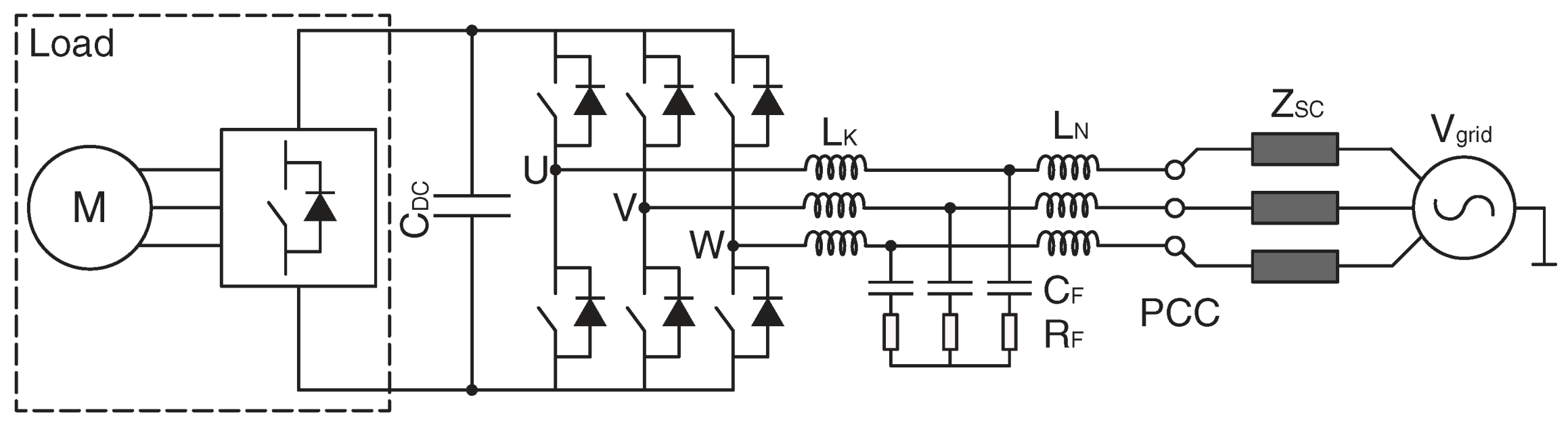
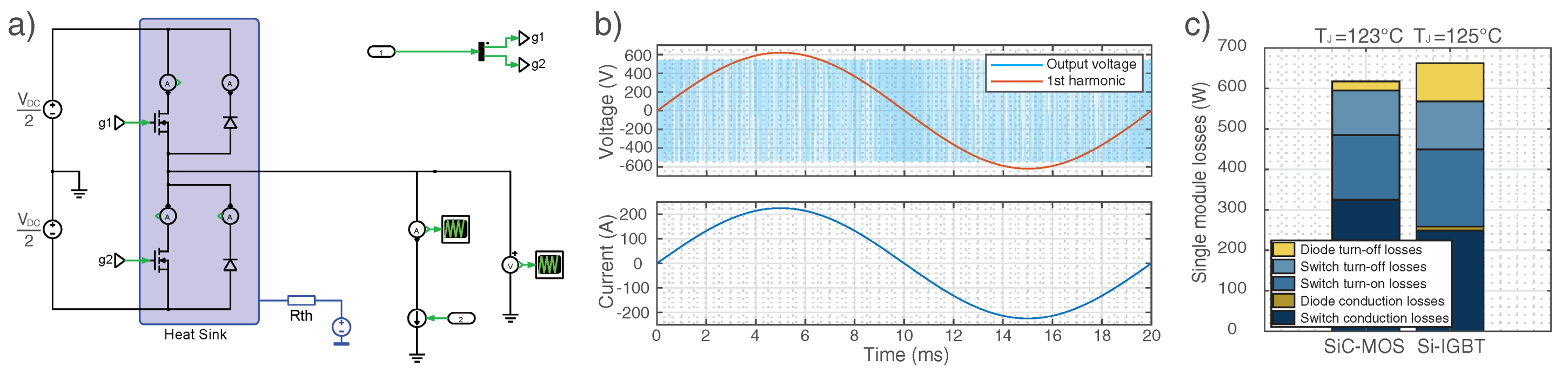
Therefore, in this work, a comparison between SiC- and silicon-based three-phase two-level voltage source converter design (2L-VSC) operating as infeed for general purpose industrial applications is performed based on transparent industry requirements, norms and design criteria. The design of inductors, capacitors and converter cooling assumes components available on the market. This aims at obtaining a fair, pragmatic comparison of the two converter designs, with the goal of identifying the potential impact that the usage of different semiconductor technologies could present in 690 V grid-connected industrial applications. The framing of these results is just as important, and hence a clear description of corresponding constraints and limitations of these results is provided. The (1700 V, 300 A) half-bridge Si-IGBT module FF300R17ME4 from Infineon was chosen for the silicon-based design, since this module is often applied in 690 V industrial converters (e.g., for drives, active front end converters, etc.). For the SiC converter, the (1700 V, 250 A) half-bridge SiC-MOSFET module BSM250D17P2E004 from Rohm was selected since this module provides the same voltage class, similar nominal ratings and thermal characteristics and uses the same module package format the Si-IGBT module features. The converter design applies results from an experimentally obtained characterization of the switching behavior of both devices [13]. Note that the designs have not been implemented.
The main contributions of this work is to demonstrate through this comparison methodology that SiC devices have the potential to be a cost-effective solution for general purpose grid-connected 690 V industrial applications, which is in itself a new result, as SiC converters are not being actively considered for these applications so far.
The paper is organized as follows. In Section 2, a definition of the converter requirements and design constraints is presented. In Section 3, each step of the converter design is introduced. Here, in each corresponding subsection, the selected switching devices are presented, the gate unit structure and functions are shown, the converter thermal design is discussed, DC-link requirements and design are depicted and the output filter design requirements, conceptualization and implementation is presented. In Section 4, the final theoretical physical layout of both converters is shown. In Section 5, a comparison of significant criteria of both converters is discussed. Finally, in Section 6, the main conclusions of the work are summarized.

2. Requirements and Design Constraints of the Two-Level Voltage Source Converter for Industrial Applications

Industrial medium and high power converters are widely distributed in electrical drives and power supplies. For the comparison of converters with SiC-MOSFETs and Si-IGBTs, a (690 V, 190 kVA) two-level voltage source converter (2L-VSC) as active front end (AFE) of an electrical drive (Figure 1 and Table 1) was selected, as the 2L-VSC is the dominating converter topology in low voltage applications ( U l l 1000 V ) [14,15].
The low switching losses of the SiC-MOSFETs enable an increase of the switching frequency from 2.25 kHz, which is a typical switching frequency for Si-IGBTs in electrical drives, to 20 kHz for SiC-MOSFETs at comparable efficiency and semiconductor losses at the defined operation point. This increased switching frequency in the AFE configuration enables a smaller and more cost-effective grid filter for the converter with SiC-MOSFETs and an operation outside of the audible noise spectrum. On the other hand, the switching frequency of the IGBT converter at the defined nominal point generates about the same maximum average junction temperature of T J , a v , m a x = 125 ° C as in the SiC-MOSFET converter, hence allowing a comparison for identical power output while operating the modules to a reasonable extent of their maximum ratings. The nominal DC-Link voltage of U D C , n = 1080 V was selected based on the work in [16,17] to ensure a 10% over the minimum voltage required to control grid currents assuming space vector modulation (SVM), and the physical design of the DC-Link was performed to ensure low parasitic inductances to reduce di/dt based overvoltages at switching transients. The grid standards VDE-AR-N 4100 and EN61000-2-2(+A1/A2) were selected to define harmonic emission limits, as both standards cover the connection to low voltage grids and provide clear emission limits for both converter designs (up to 9 and 150 kHz, respectively). As grid-side filter topology, a conventional LCL-Filter structure with passive damping was selected.
The methodology of this work was to define a fair operation point for both designs and to then design the converter parts and summarize their characteristics. The selection of the operation point was based on the experimental data the corresponding module characterizations provided. With them, and datasheet-based transient thermal impedance and device forward characteristics, simulations of junction temperatures were performed to observe the maximum current that would be possible to obtain from the modules as a function of case-to-ambient thermal resistance (cooling solution) and switching frequency.
The (1700 V, 300 A) silicon IGBT halfbridge module from Infineon, which is widely distributed in industrial drives and the (1700 V, 250 A) SiC-MOSFET halfbridge module from Rohm where chosen as power semiconductors for the comparison. To calculate the converter power and operate both modules to a reasonable extent of their maximum ratings, a maximum average junction temperature of T J , a v , m a x = 125 °C and a maximum ambient temperature of T a m b = 45 °C were assumed. Both temperatures are typical for the design of industrial converters, as T J , a v , m a x = 125 °C presents a reasonable margin to the maximum operation temperature under switching conditions power modules typically present ( T J , o p = 150 °C), and T a m b = 45 °C is a typical temperature to present the nominal characteristics of an industrial inverter without the need for derating. During the search of a fair nominal operation point for design, it was identified that an identical cooling solution consisting of heatsink and fan featuring a thermal resistance of R t h c a = 0.02867 K / W could be used. This simplifies the converter comparison and allows both designs to perform with identical power output and nominal current, presenting T J , a v , m a x   125 ° C at the critical operation point while operating at reasonable switching frequencies for both filter designs. For the Si-IGBT, a fair switching frequency meant that no carrier bands should fall below 2 kHz, as this would unfairly generate a bulky filter due to stricter harmonic emission requirements. Additionally, standard switching frequencies for industrial AFEs were preferred. On the other hand, a fair switching frequency for the SiC-MOSFET meant that at the required nominal current runs the module close to a reasonable extent of its maximum ratings (not under use the module), while also allowing standard core materials for filter design. Hence, 2.25 and 20 k H z were selected for the Si- and SiC-based converter designs, respectively, and their critical operation point was characterized by nominal current, a modulation index of M = 1.15 and unity power factor ( c o s ( φ ) = 1 ) feeding energy into the grid, as observed in Figure 2.
These thermal requirements and loss results were obtained by calculating the semiconductor losses of the converter based on experimental characterization of the switching loss as in [13] and using on-state characteristics and transient thermal impedance curves as provided in the corresponding datasheets. The corresponding gate resistances for both designs were [ R G ( o n ) , R G ( o f f ) ] = [ 0.8 Ω , 0.6 Ω ] and [ 3.3 Ω , 4.7 Ω ] for the SiC-MOSFET module and the Si-IGBT module, respectively.
Then, nominal operation point and the previously defined converter requirements were used to design all the corresponding converter parts. Finally, all designed requirements were either matched with a part in the market (capacitors) or directly discussed with manufacturers (cooling system, power modules and filter inductors) to obtain a realistic design. These parameters were then summarized, and weight, volume, losses and cost analyses were performed. A summary of the methodology used in this design and corresponding comparison is shown in Figure 3.
Considering the converter comparison, the ratio of converter costs and power (costs/kVA) is the most important requirement and comparison criteria for industrial converters. Further important requirements and comparison criteria are efficiency and power density (size/power). A fair comparison of two converters with different power semiconductors is a complex task which can be realized for different conditions and criteria. In this paper, the converter comparison is performed such that both converters provide the same nominal power in the nominal converter operating point using identical cooling solutions.
This approach enables a direct comparison of converter component costs, efficiency and power density assuming power semiconductors in an identical module and at identical cooling conditions. Considering the material costs the SiC converter realizes a higher switching frequency and a smaller LCL-Filter with potentially lower filter costs which could compensate the higher power semiconductor costs. All provided costs are referential, and they were obtained from price comparing websites such as octopart [18] or directly from manufacturers between July and August 2020. Prices in Euros were translated to USD (1 Euro = 1.2 USD).

3. Power Converter Design

3.1. Switching Device Selection

The devices were selected to feature similar electrical ratings, thermal characteristics and identical package dimensions (Figure 4 and Table 2), providing good grounds for a fair comparison. Both devices were studied by Fuentes et al. [13], with particular focus to the characterization of their switching behavior. To calculate losses, experimental data regarding the switching losses [13] and datasheet on-state characteristics were applied. Plecs-Matlab based simulations based on the concept presented in [13] were performed to determine the maximum case temperature to achieve junction temperatures averaging 125 °C as a function of switching frequency and phase current. The resulting case temperatures and module loss were in turn used to determine the required case to ambient thermal resistance R t h c a , which is the major input parameter for the thermal design.

3.2. Gate Unit Requirements

The gate unit concept is presented in Figure 5. Important boundary conditions and requirements for both designs are presented in Table 3. The realization of suitable gate voltages ( U G S / G E along with required peak gate currents at minimum power losses are the basic gate unit requirements. The corresponding equations for these calculations are straightforward and can be found in [21]. Additionally, it is of particular importance for the SiC device that parasitic inductances in the driving loop are minimized. This means the driver needs to be as close to the driving pins as possible and overlapping driving/return current paths are desired [22]. DC/DC converters with a small coupling capacitance are also required to reduce common mode currents crossing the isolation barrier. Short circuit detection is also desired and can be implemented for both technologies by the DESAT detection method [23] with soft turn-off, considering that for the SiC-MOSFETs the complete detection/protection process should not last more than 3 μs [24]. Additional considerations such as crosstalk attenuation and active clamping can be considered, but no related effects during the characterization process were observed, thus no countermeasures were included in this particular design. Cost estimations were based on required isolated DC/DC power supply with isolation capability for 1700 V devices, optocouplers, ceramic capacitors and PCB costs.

3.3. Thermal Design

The main criteria for the thermal design is the required case to ambient thermal resistance defined as:
R t h c a = T c T a m b 3 P ,
in which P represents single module losses. Please note both designs share the same nominal power and required R t h c a , but they do not have the same case temperatures or losses, as observed in Figure 2. To fulfill the required R t h , an effective cooling solution comprised of the sum of thermal compound and heatsink thermal impedances was defined. The components of the cooling solution can be found in Table 4.
As thermal compound, a silicon-based thermal paste, the Wacker P12 [25], was selected as its characteristics are suitable for module applications [26,27]. Additionally, it was considered that, due to chip positioning in the module, not the entire baseplate area is used for heat transfer, hence 90% of the total baseplate area was considered for the thermal resistance calculation.
Heatsinks and fan-based air cooling are a widely distributed cooling solution in industrial converters, and hence this cooling solution was selected. However, due convection heat transfer, a simple calculation of the thermal resistance based on thickness and area is typically not possible, and high heatsink surface area usage is recommended [28] as typically the whole heatsink surface is heated up for its characterization. Several heatsinks were considered, but finally the forced cooling aggregated heatsink LA HL 3200 from Fischer Elektronik [29] was selected, as its thermal resistance was determined with smaller devices compared to the modules being considered (80 × 43 m m 2 ), and hence the nominal datasheet parameters can be considered as a worst case scenario. A diagram of the corresponding heatsink can be found in Figure 6.

3.4. DC-Link Design

The DC-Link has the task of acting as energy storage and providing a stable voltage for modulation purposes. The calculation of its capacitance can be carried out considering several requirements such as voltage ripple, ride-through capability and stored energy for control requirements. From those three, capacitor ripple requirements tend to result in small capacitance values for reasonable voltage ripple limits. This is particularly true for SiC based designs, as they tend to feature higher switching frequencies, which impact capacitance requirements significantly, as can be confirmed by the calculation methods proposed in [30]. Voltage ride-through capability typically sets tougher DC-Link capacitance requirements, as it is important that the converter does not trigger shutdown for low DC-Link voltage value due to milliseconds-long grid voltage dips. However, since the required ride-through time and minimum allowable DC-Link voltage can vary from design to design, a different criterion was considered to better represent industrial inverters. An important index to characterize the DC-Link capacitor stored energy of a power converter is its energy to power W s k V A ratio [31], which represents the time a converter loses its DC-Link stored energy at constant nominal power. In this study, the index was selected as t r a t i o = 8 W s k V A , which is a typical value for film capacitors in industrial electrical drives with active front end. Hence, the DC-Link capacitance can be obtained from the W s k V A ratio as:
C D C = U l l I L 3 · 0.001 · t r a t i o 1 2 U D C , n 2 ,
which yields a capacitance of C D C = 2.6 m F .
Regarding RMS current requirements, the worst case scenario was calculated based on the work in [32], resulting in I C , R M S = 79.55 A .
Due to their superior low stray inductance and their additional reliability advantages [33], film capacitors were selected for both converter designs. This assumption enables a comparison of converters without the influence of deviating capacitor technologies. Due to its form factor, capacitance and weight, the metallized polypropylene film capacitor FFLI6U0267KJE from AVX [34] was selected for this study, which suits perfectly to reach the desired capacitance, while also fulfilling RMS current requirements.
Finally, the DC-Link bus was designed with 2 mm thick copper bars isolated through a 0.25mm Hostaphan RN foil [35]. The DC-Link concept also features a small distance between the capacitor bank to the module connections, to homogenize the observed stray inductance from all module connections and distance itself from the heat sources. This space is however small, to not substantially increase stray inductance. Simulations with Altair Flux 2018 were performed to estimate the DC-Link stray inductance, from which an inductance of 15 ± 0.5 n H from every module connection was obtained. A summary of the DC-Link design and corresponding diagrams can be found in Table 5 and Figure 7, respectively.

3.5. Filter Design

3.5.1. Grid Codes and Models

The main function of the grid side filter is to keep the harmonic emission in compliance with grid codes. Especially in the frequency range f h > 2 kHz, called supraharmonics, the definition of harmonic emissions has been a continuous process over the last years. For a comparable filter design, three harmonic emission limits were considered for the filters to comply with: the harmonic limits of VDE-AR-N 4100, IEC/TS 62578 and EN61000-2-2 [36,37,38]. Usually, the standard EN61000-2-2 contains only compatibility levels for external voltage distortion, which can be used for filter design with 3 dB safety margin. In the standard IEC/TS 62578, recommendations for harmonic voltage emissions up to 150 kHz are proposed. In the standard VDE-AR-N 4100, emission limits for harmonic voltages and currents are given up to 9 kHz, with the remark that, if the harmonic current limits are not met, it is only necessary to meet the harmonic voltage limits. Therefore, only the harmonic voltage limits are considered for the filter design. The filters must mitigate the harmonic emissions below all considered standards. Figure 8 shows a comparison of the allowable voltage distortion at the point of common coupling (PCC).
To calculate the voltage distortion at the PCC, the grid impedance Z ̲ SC has to be considered. The usual approach to assume a purely inductive grid would lead to bulky and expensive filters, which are not necessary in realistic grid applications. In the document CISPR11 [39], a network for harmonic emission measurement is defined. In the standard IEC/TS 62578, a grid impedance is proposed, which is based on measured grid data. Figure 9 shows a comparison of the different grid models. The network defined in [39] is not valid for low frequencies. Hence, a combined frequency dependent grid impedance model
Z ̲ SC = j ω h L SC for f h < 1 kHz 50 Ω | | ( 5 Ω + j ω h 50 μ H ) for f h > 1 kHz
is used for the filter design. For low frequencies, a purely inductive weak grid with a relative short circuit power of rsc = 10 is still assumed, which leads to a grid inductance of L SC = 1.4 mH. For all harmonic frequencies, the grid impedance is higher than the approximation that is given in [38], which leads to an additional safety margin.

3.5.2. Filter Design

Regarding filter design, there is a variety of possible filter solutions. For the damped LCL-Filter (Figure 1), there are the free filter parameters L K , L N , C F , Y , R F . Because a detailed filter design is beyond the scope of this paper, a few useful simplifications are applied, based on commercial available LCL-Filters [40,41]. Unfortunately, for the selected voltage rating and PWM frequency, no commercial filters are available. Therefore, an industrial-based filter design is presented in this section.
A damping resistor
R F = 2 D L K L N C F , Y ( L K + L N )
with a weak damping ratio of D = 0.1 is used. This ratio is chosen as compromise between harmonic reduction and losses.
In commercially available filters, both damped and undamped filters are offered. Undamped filters usually require an active damping algorithm. A possible active damping solution can be found, e.g., in [42,43].
In commercial filters, an inductance ratio of
L N L K 2
is often realized, which keeps good compromise between detuning resonant frequency because of grid impedance, converter current ripple and stored energy in the filter.
Considering (4) and (5), two free filter parameters exist. For the following filter design, a grid-search method is used, where the parameters L K and C F , Y are varied within a reasonable range. For each pair, the damping behavior of the filter can be calculated and it is checked if the harmonic limits are met.
For stability reasons, the resonant frequency
ω res = 2 π F res = 1 C F , Y 1 L K + 1 L N
is limited to
500 Hz F res f sw 2
as stated in [44].
The voltage distortion at PCC can be calculated with
| U ̲ PCC , h | = | Z ̲ F Z ̲ SC Z ̲ F ( Z ̲ N + Z ̲ SC ) + Z ̲ K ( Z ̲ F + Z ̲ N + Z ̲ SC ) | | U ̲ SR |
and
Z ̲ F = R F + 1 j ω h C F , Y
Z ̲ K = j ω h L K
Z ̲ N = j ω h L N ,
and the frequency dependent grid impedance Z ̲ SC ( ω h ) . Because of superposition, each frequency can be calculated separately. These impedances and the voltage at the point of common coupling can be found for clarity in Figure 10.
In (7), the complex variable U ̲ SR refers to a so-called worst-case amplitude spectrum. The PWM based converter harmonics depend on the modulation index, respective of the fundamental output voltage [45]. Hence, the harmonic spectra for minimum, nominal and maximum fundamental output voltage of the converter are used. For each harmonic component, the maximum harmonic emission of the spectra is applied to the filter design, as:
| U ̲ SR , h | = max ( | U ̲ SR , min , h | ; | U ̲ SR , nom , h | ; | U ̲ SR , max , h | ) ,
where index h indicates the h-harmonic frequency.
Regarding the grid codes, the fundamental voltage can vary between 90 % (min) and 110 % (max) of the nominal voltage at 690 V .
To achieve the harmonic spectra, simulations or analytical calculations can be used [46]. Creating the spectra by simulation has the advantage that the influence of deadtime effects in the harmonic spectrum can be considered easily [47] (see Figure 11). The filter design is based on calculating differential-mode components in the line to ground voltage harmonics (using worst case spectrum) at the PCC for both designs and compared with the standards to constrain the design. Common-mode components in the spectra are not considered for the LCL-Filter design. It is assumed that both converters feature a suitable common mode filter concept which is out of the scope of this paper since it depends on various details of the grid and load side converter as well as the load including grounding concept, cable connections, etc. The resulting worst-case spectrum for the both converter designs is shown in Figure 11. Both designs feature different deadtimes due to their corresponding switching times. Note that the selected switching frequency does not affect first carrier bands of the Si-IGBT design at 2 kHz, hence validating that the filter design effort must only comply with supraharmonic emission limits.
Calculation the grid voltage distortion (7) and checking the compliance with the chosen grid codes (Figure 9) still leads to a large variety of filter solutions. Figure 12 shows a cutout of possible filter realizations. For clarity, it shows the necessary filter capacity in star-connection and the sum of grid- and converter-side inductance considering (5). The colored crosses indicate the selected filter parameters, red and blue for the LCL-filters for the SiC and Si designs, respectively. The selection is based on minimizing the stored energy in the filter components, defined as:
E Filter = 1 2 C F , Y U ^ N , LE 2 + ( L K + L N ) I ^ N , rated 2 ,
where U ^ N , LE is the peak grid phase-neutral voltage and I ^ N , rated is the peak current at the grid side of the filter.
The nominal values of the comparable filter elements are summarized in Table 6. In cooperation with the manufacturer of inductive components Schmidbauer [48], a mechanical realization for the inductive filter components was designed. Regarding the corresponding capacitors, TDK EPCOS capacitors for AC filtering—from the B32370 and B32374 families for the SiC and Si converters, respectively—were selected to realize the filter capacitors [49]. Finally, chassis mounted resistors from Arcol line HS 150 were selected for damping, These resistors are able to operate at 45 W without a heatsink. The design summary can be found in Table 7.

4. Physical Layout Summary

A theoretical physical layout of the converter and its LCL-filter, including their main components are presented in Figure 13. The modules are distributed to be centered to the corresponding fans and to observe a similar DC-Link stray inductance from their connection points. Both the air exhaust and the DC-Link support structure are included for reference purposes only. No support structures, cables or additional protection measures were numerically considered for this study to focus on the functional parts. This is also an important constraint. As a result, percentage weight and costs gains would be lower as more elements common to both structures are included in the study.
Due to the comparison of the defined functional parts, the main differences are caused by the different power semiconductors and the filter design. The corresponding LCL-Filter designs are presented in Figure 13, and, as can be observed in the figure, the SiC converter presents important filter reductions when compared to the Si-based converter design. Filter volume and weight are reduced by almost two thirds while its overall cost is reduced by 56% (see Table 7).

5. Comparison of Resulting Inverters

Finally, the comparison of both designs regarding loss, efficiency, weight and cost is performed. Regarding loss calculations, both rectifier and inverter operation for different loads at unity power factor and using a modulation index M = 1.1547 (critical scenario) were considered. The results are presented in Figure 14. As mentioned in Section 2, the critical design point presents itself in unity power factor by inverter operation, where both the IGBTs and the MOSFETs average junction temperatures set the design boundaries. Here, it can be observed how, due to the smaller die area (higher current density), the SiC-MOSFET presents higher junction thermal oscillation than the Si-IGBT counterpart, while still remaining within safe operation. However, in rectifier operation, due to the silicon diode loss characteristics of the Si-IGBT module, and the current sharing characteristic between the MOSFET channel and the diode due to active rectification (which can be observed in the loss distribution of the SiC-MOSFET design), both devices present lower average junction temperatures. The SiC device observes switch and diode average junction temperatures of [104 92] °C, respectively, in contrast with the Si-IGBT module which presents [110 118] °C in rectifier operation at nominal current and M = 1.1547 . Regarding filter losses, to estimate its losses at lower currents, inductor losses provided by manufacturer at nominal operation were supposed to be equally distributed between copper and core losses. This is a useful assumption for a first level loss estimation. With this assumption, a winding resistance is calculated using the copper losses at nominal operation. Losses at lower currents were calculated for the resulting winding resistance assuming constant core losses. As observed in Figure 14, both converter losses are outshined by filter losses for low currents. Hence, efficiency could be increased by a loss optimized filter design. However, this would also influence costs, weight and volume of the filter.
When translating these losses into efficiency (see Figure 15), it can be observed that the SiC variant outperforms the Silicon based converter within the whole operation range, being also negatively affected by the filter for light loads, but presenting an overall behavior over 98% efficiency for almost the entire operation range. Furthermore, the current sharing of the MOSFET and diode in rectifier operation further reduces losses (see Figure 14), presenting an efficiency of 98.9% at nominal operation point. Regarding the Si-IGBT based design, the larger filter, the diode reverse recovery, the slower IGBT switching transients and the IGBT forward voltage drop characteristic are the main factors of reduced efficiency at light loads, performing better the closer is the device to reaching nominal operation with 98.3% efficiency at nominal rectifier operation.
Considering the weight comparison analysis (see Figure 16), it is a known fact that a significant part of the converter weight is caused by the inductive line components (filter inductors and line transformer) because of their magnetic cores and the windings which are mainly composed of iron and copper in industrial converters. Hence, by raising the switching frequency almost tenfold, a significant reduction of the inductor weight by 68% is achievable assuming the harmonic limits in Figure 8. This heavily impacts the total weight of the converter, allowing a power density of 1.97 kVA/kg vs. 0.77 kVA/kg for the main components of the SiC-MOSFET and Si-IGBT converter, respectively.
Finally, the cost distribution comparison of all converter components can be found in Figure 17. It is interesting that the sum of the considered component costs of the SiC-MOSFET converter is reduced by about 10% compared to that of the Si-IGBT converter. This cost difference is not substantial, and both designs share several design choices. The differences originate in the trade-off between module and filter costs. Here, due to the high share of the filter costs, the Si-IGBT-based converter components ends up being 10% more expensive than the SiC based-variant despite the lower semiconductor costs, showcasing the substantial impact of the filter on the overall design.
To evaluate these results, the total converter costs should be considered. The total converter costs depend on further elements such as the cabinet, control platform, switches, sensors, cables and common-mode filter. Additionally, heavier components imply additional structural costs for the IGBT design, while the common-mode filter could also impact the cost of the SiC design. The evaluation a full EMI solution was considered out of scope for this work, as, to perform an EMI analysis, the common-mode filter should be also included, and this filter must consider several additional aspects such as the mechanical layout, cable shielding and lengths and grounding concept in order to define the final solution. Furthermore, regarding industrial applications, an additional norm to evaluate higher frequency emissions would have to be considered.
Additionally, cost reductions of the considered main components are possible for both designs. Obvious examples for cost reductions of Si-based converter components are less costly gate drive units due to reduced dv/dt immunity requirements and DC-Link capacitors if electrolytic-based capacitors are applied. However, the results of considered components indicate that SiC-based converters have the potential to provide a cost-effective solution while offering further attractive features such as an increase of efficiency and power density compared to Si-based converters. This is remarkable, as industrial active front end converters have not been high on the list of applications that could benefit of SiC module usage (e.g., [50]).

6. Conclusions

In this paper, a comparison of the main components of two grid-tied 190 kVA 2L-VSCs based on silicon carbide (SiC)-MOSFETs and silicon (Si)-IGBTs for 690 V grids is performed. The main components include comparable 1700 V SiC-MOSFET and Si-IGBT modules, the gate drive units, the DC-Link and the grid side LCL-Filter design. The comparison is based on the experimental characterization of the switching behavior and datasheet values for the on-state behavior of the SiC-MOSFET and Si-IGBT modules. The results show that the weight and material costs of the considered components of the SiC-MOSFET converter are reduced by 39% and 10.9% when compared with the silicon based solution, while providing superior efficiency (>0.5%) in the entire operating range. This shows that SiC-MOSFETs offer the potential of a cost competitive solution with the additional benefits of higher efficiency, power density and switching frequency over the hearing range. This corresponds very well to the development trends of industry applications.

Author Contributions

Conceptualization, C.D.F., M.M. and S.B.; methodology, C.D.F. and M.M.; software, C.D.F. and M.M.; formal analysis, C.D.F. and M.M., writing—original draft preparation, C.D.F. and M.M.; writing—review and editing, S.K. and S.B.; visualization, C.D.F. and M.M.; and supervision, S.B. All authors have read and agreed to the published version of the manuscript.

Funding

Open access funding was partially provided by the Publication Fund of the TU Dresden.

Acknowledgments

This work was supported in part by the ANID (CONICYT-PCHA/Doctorado Nacional/2015-21151279), in part by the DAAD, in part by the Technische Universität Dresden, in part by AC3E (ANID/Basal/FB0008), and in part by SERC (ANID/FONDAP/15110019).

Conflicts of Interest

The authors declare no conflict of interest.

References

  1. She, X.; Huang, A.Q.; Lucia, O.; Ozpineci, B. Review of Silicon Carbide Power Devices and Their Applications. IEEE Trans. Ind. Electron. 2017, 64, 8193–8205. [Google Scholar] [CrossRef]
  2. Abbatelli, L.; Macauda, M.; Catalisano, G.; Boscarato, A.; Kohout, D. Cost Benefits on High Frequency Converter system based on SiC MOSFET approach. In Proceedings of the PCIM Europe 2014, International Exhibition and Conference for Power Electronics, Intelligent Motion, Renewable Energy and Energy Management, Nuremberg, Germany, 20–22 May 2014; pp. 1–5. [Google Scholar]
  3. Moxey, G.; Scalia, P. Presentation: Enabling and Expanding Broader Power Markets with Wolfspeed Silicon Carbide. In Proceedings of the Power Electronics Conference, Busan, Korea, 27–31 May 2019. [Google Scholar]
  4. Perdikakis, W.; Hall, B.; Scott, M.; Kitzmiller, C.; Yost, K.J.; Sheets, K.A. Comparison of Si and SiC EMI and Efficiency in a Two-level Aerospace Motor Drive Application. IEEE Trans. Transp. Electrif. 2020, 6, 1401–1411. [Google Scholar] [CrossRef]
  5. Burkart, R.M.; Kolar, J.W. Comparative Life Cycle Cost Analysis of Si and SiC PV Converter Systems Based on Advanced η-ρ-σ Multiobjective Optimization Techniques. IEEE Trans. Power Electron. 2017, 32, 4344–4358. [Google Scholar] [CrossRef]
  6. Stepenko, S.; Husev, O.; Vinnikov, D.; Roncero-Clemente, C.; Pimentel, S.P.; Santasheva, E. Experimental Comparison of Two-Level Full-SiC and Three-Level Si–SiC Quasi-Z-Source Inverters for PV Applications. Energies 2019, 12, 2509. [Google Scholar] [CrossRef] [Green Version]
  7. Wolski, K.; Zdanowski, M.; Rabkowski, J. High-Frequency SiC-Based Inverters With Input Stages Based on Quasi-Z-Source and Boost Topologies—Experimental Comparison. IEEE Trans. Power Electron. 2019, 34, 9471–9478. [Google Scholar] [CrossRef]
  8. Whitaker, B.; Barkley, A.; Cole, Z.; Passmore, B.; Martin, D.; McNutt, T.R.; Lostetter, A.B.; Lee, J.S.; Shiozaki, K. A High-Density, High-Efficiency, Isolated On-Board Vehicle Battery Charger Utilizing Silicon Carbide Power Devices. IEEE Trans. Power Electron. 2014, 29, 2606–2617. [Google Scholar] [CrossRef]
  9. Rujas, A.; Lopez, V.M.; Garcia-Bediaga, A.; Berasategi, A.; Nieva, T. Railway traction DC-DC converter: Comparison of Si, SiC-hybrid, and full SiC versions with 1700V power modules. IET Power Electron. 2019, 12, 3265–3271. [Google Scholar] [CrossRef]
  10. Gant, L.; Banerjee, S.; Zhang, X.; Sheh, G.; Lemmon, A.; Shahabi, A. System Level Comparison of Si IGBTs and SiC MOSFETs. In Proceedings of the PCIM Europe 2017, International Exhibition and Conference for Power Electronics, Intelligent Motion, Renewable Energy and Energy Management, Nuremberg, Germany, 16–18 May 2017; pp. 1–8. [Google Scholar]
  11. Mirzaee, H.; De, A.; Tripathi, A.; Bhattacharya, S. Design comparison of high power medium-voltage converters based on 6.5 kV Si-IGBT/Si-PiN diode, 6.5 kV Si-IGBT/SiC-JBS diode, and 10 kV SiC MOSFET/SiC-JBS diode. In Proceedings of the 2011 IEEE Energy Conversion Congress and Exposition, Phoenix, AZ, USA, 16–21 September 2011; pp. 2421–2428. [Google Scholar]
  12. Sato, I.; Hori, M.; Tanaka, T.; Yamada, R.; Toba, A. A High Power Density Inverter Utilizing SiC-MOSFET and Fair Comparison Method of the Same Kind of Power Converters. In Proceedings of the PCIM Europe Digital Days 2020, International Exhibition and Conference for Power Electronics, Intelligent Motion, Renewable Energy and Energy Management, Nuremberg, Germany, 7–8 July 2020; pp. 1–6. [Google Scholar]
  13. Fuentes, C.D.; Kouro, S.; Bernet, S. Comparison of 1700-V SiC-MOSFET and Si-IGBT Modules Under Identical Test Setup Conditions. IEEE Trans. Ind. Appl. 2019, 55, 7765–7775. [Google Scholar] [CrossRef]
  14. Toledo, S.; Rivera, M.; Maqueda, E.; Ayala, M.; Pacher, J.; Romero, C.; Gregor, R.; Dragicevic, T.; Wheeler, P. Multi-modular scalable DC-AC power converter for current injection to the grid based on predictive voltage control. In Proceedings of the 2019 IEEE 15th Brazilian Power Electronics Conference and 5th IEEE Southern Power Electronics Conference (COBEP/SPEC), Sao Paulo, Brazil, 1–4 December 2019; pp. 1–6. [Google Scholar]
  15. Chatterjee, P. Design Considerations for fast DC Chargers Targeting 350 Kilowatt. Power Electron. Eur. 2019, 2, 33–35. [Google Scholar]
  16. Abu-Rub, H.; Malinowski, M.; Al-Haddad, K. Power Electronics for Renewable Energy Systems, Transportation and Industrial Applications; John Wiley and Sons: Hoboken, NJ, USA, 2014. [Google Scholar]
  17. Rivera, S.; Wu, B.; Kouro, S. Distributed dc bus EV charging station using a single dc-link h-bridge multilevel converter. In Proceedings of the 2014 IEEE 23rd International Symposium on Industrial Electronics (ISIE), Istanbul, Turkey, 1–4 June 2014. [Google Scholar] [CrossRef]
  18. Octopart. Search Engine for Electronic Parts. Available online: https://octopart.com/ (accessed on 17 August 2020).
  19. Infineon Technologies. Datasheet: 1700V Si-IGBT Halfbridge Module FF300R17ME4; Infineon Technologies: Neubiberg, Germany, 2014. [Google Scholar]
  20. ROHM. Datasheet: 1700V SiC-MOSFET Halfbridge Power Module BSM250D17P2E004; ROHM: Kyoto, Japan, 2016. [Google Scholar]
  21. Toshiba. Application Note: MOSFET Gate Drive Circuit; Technical Report; Toshiba Electronic Devices & Storage Corporation: Tokyo, Japan, 2018. [Google Scholar]
  22. Colmenares, J.; Peftitsis, D.; Rabkowski, J.; Sadik, D.; Tolstoy, G.; Nee, H. High-Efficiency 312-kVA Three-Phase Inverter Using Parallel Connection of Silicon Carbide MOSFET Power Modules. IEEE Trans. Ind. Appl. 2015, 51, 4664–4676. [Google Scholar] [CrossRef]
  23. Rice, J.; Mookken, J. SiC MOSFET gate drive design considerations. In Proceedings of the 2015 IEEE International Workshop on Integrated Power Packaging (IWIPP), Chicago, IL, USA, 3–6 May 2015; pp. 24–27. [Google Scholar]
  24. Infineon Technologies. AN2017-04: Advanced Gate Drive Options for Silicon-Carbide (SiC) MOSFETs Using EiceDRIVER(TM); Technical Report; Infineon Technologies: Neubiberg, Germany, 2017. [Google Scholar]
  25. Wacker. Datasheet: Wacker Silicone Paste P12; Technical Report; Wacker: Munich, Germany, 2020. [Google Scholar]
  26. Freyberg, M.; Daucher, C. Application of Thermal Paste for Power Modules without Base Plate, Version 1.0; Technical Report; Semikron International: Nuremberg, Germany.
  27. Drexhage, P.; Beckedahl, P. AN 18-001: Thermal Paste Application; Technical Report; Semikron International: Nuremberg, Germany, 2018. [Google Scholar]
  28. Wintrich, A. Application Manual Power Semiconductors; ISLE Verlag: Ilmenau, Germany, 2015. [Google Scholar]
  29. Fischerelektronik. Datasheet: LA HL 3 200; Technical Report; Fischerelektronik: Ludenscheid, Germany, 2020. [Google Scholar]
  30. Chen, T.; Li, S.; Fahimi, B. Analysis of DC-Link Voltage Ripple in Voltage Source Inverters without Electrolytic Capacitor. In Proceedings of the IECON 2018—44th Annual Conference of the IEEE Industrial Electronics Society, Washington, DC, USA, 21–23 October 2018. [Google Scholar] [CrossRef]
  31. Rodriguez, J.; Wu, B.; Bernet, S.; Zargari, N.; Rebolledo, J.; Pontt, J.; Steimer, P. Design and Evaluation Criteria for High Power Drives. In Proceedings of the 2008 IEEE Industry Applications Society Annual Meeting, Edmonton, AB, Canada, 5–9 October 2008; pp. 1–9. [Google Scholar] [CrossRef]
  32. Kolar, J.W.; Round, S.D. Analytical calculation of the RMS current stress on the DC-link capacitor of voltage-PWM converter systems. IEE Proc Electr. Power Appl. 2006, 153, 535–543. [Google Scholar] [CrossRef] [Green Version]
  33. Wang, H.; Blaabjerg, F. Reliability of Capacitors for DC-Link Applications in Power Electronic Converters-An Overview. IEEE Trans. Ind. Appl. 2014, 50, 3569–3578. [Google Scholar] [CrossRef] [Green Version]
  34. AVX. Datasheet: Medium Power Film Capacitors FFLI 800V to 1400 Vdc; AVX: Fountain Inn, SC, USA, June 2015. [Google Scholar]
  35. Mitsubishi. Datasheet: Transparente Polyesterfolie Hostaphan RN 50-350 Mitsubishi Polyester Film GmbH; Mitsubishi: Wiesbaden, Germany, January 2019. [Google Scholar]
  36. DIN EN 61000-2-2 VDE 0839-2-2:2019-06 Elektromagnetische Vertraeglichkeit (EMV)Teil 2-2: Umgebungsbedingungen—Vertraeglichkeitspegel fuer Niederfrequente Leitungsgefuehrte Stoergroessen und Signaluebertragung in oeffentlichen Niederspannungsnetzen; VDE: Berlin, Germany, June 2019.
  37. VDE-AR-N 4100 Anwendungsregel:2019-04 Technische Regeln fuer den Anschluss von Kundenanlagen an das Niederspannungsnetz und deren Betrieb (TAR Niederspannung); VDE: Berlin, Germany, April 2019.
  38. IEC TS 62578:2015. Power Electronics Systems and Equipment—Operation Conditions and Characteristics of Active Infeed Converter (AIC) Applications Including Design Recommendations for Their Emission Values below 150 kHz; IEC: Geneva, Switzerland, 2015. [Google Scholar]
  39. IEC. CISPR 11:2015+AMD1:2016+AMD2:2019 Industrial, Scientific and Medical Equipment—Radio-Frequency Disturbance Characteristics–Limits and Methods of Measurement; IEC: Geneva, Switzerland, 2015. [Google Scholar]
  40. Schaffner. DATASHEET FN 6840: LCL Filters for Active Front End Motor Drives and Active Infeed Converter; Schaffner: Luterbach, Switzerland, 2019. [Google Scholar]
  41. TDK. Datasheet: EMC Filters, 3-Line LCL Filters, Series B84143G; TDK: Tokyo, Japan, 2017. [Google Scholar]
  42. Wagner, M.; Barth, T.; Alvarez, R.; Ditmanson, C.; Bernet, S. Discrete-Time Active Damping of LCL-Resonance by Proportional Capacitor Current Feedback. IEEE Trans. Ind. Appl. 2014, 50, 3911–3920. [Google Scholar] [CrossRef]
  43. Wang, X.; Blaabjerg, F.; Loh, P.C. Virtual RC Damping of LCL-Filtered Voltage Source Converters With Extended Selective Harmonic Compensation. IEEE Trans. Power Electron. 2015, 30, 4726–4737. [Google Scholar] [CrossRef] [Green Version]
  44. Dursun, M.; DOSOGLU, M.K. LCL Filter Design for Grid Connected Three-Phase Inverter. In Proceedings of the 2018 2nd International Symposium on Multidisciplinary Studies and Innovative Technologies (ISMSIT), Ankara, Turkey, 19–21 October 2018; pp. 1–4. [Google Scholar]
  45. Bernet, S.; Brueckner, T.; Malinowski, M.; Weber, J.; Weitendprf, N. Selbstgefuehrte Stromrichter am Gleichspannungszwischenkreis; Springer: Berlin/Heidelberg, Germany, 2012. [Google Scholar]
  46. Holmes, D. Pulse width Modulation for Power Converters: Principles and Practice; John Wiley: Hoboken, NJ, USA, 2003. [Google Scholar]
  47. Kus, V.; Josefova, T. Effect of dead times on the values of input current harmonics drawn from the grid by a voltage-source active rectifier. In Proceedings of the 2014 International Conference on Applied Electronics, Pilsen, Czech Republic, 9–10 September 2014; pp. 165–168. [Google Scholar]
  48. Schmidbauer. Inductive Components Manufacturer. Available online: https://www.schmidbauer.net/en/ (accessed on 17 August 2019).
  49. TDK. Datasheet: Film Capacitors–Power Electronic Capacitors, FilterCap MKD-AC—Single Phase; Version 4; TDK: Tokyo, Japan, December 2019. [Google Scholar]
  50. Power America. PowerAmerica Strategic Roadmap for Next Generation Wide Bandgap Power Electronics Version 1.0; Power America: Raleigh, NC, USA, 2018. [Google Scholar]
Figure 1. Circuit configuration of the proposed active front end for comparison purposes: the grid-tied 2L-VSC with LCL-Filter.
Energies 14 03054 g001
Figure 2. Selected critical operation point based on simulations and calculation of required case-to-ambient thermal resistance. (a) Plecs-based simulation using experimental data from characterization experiments [13]. (b) Critical operation point, c o s ( φ ) = 1 in inverter operation, M = 1.15 , first harmonic of the modulated voltage is shown in phase with nominal current. (c) Loss distribution of a single module and junction temperature of the critical element (switch) at the critical operation point.
Energies 14 03054 g002
Figure 3. Summary of the employed methodology used in this study to perform the converter designs and its corresponding comparison.
Energies 14 03054 g003
Figure 4. Selected half-bridge modules: (Left) (1700 V, 250 A) Infineon FF300R17ME4 (SI-IGBT + Si-Diode) [19]; and (Right) (1700 V, 250 A) Rohm BSM250D17P2E004 (SiC-Mosfet+SiC-SBD) [20].
Energies 14 03054 g004
Figure 5. Gate unit for the characterization of SiC-MOSFET and Si-IGBT modules, as presented in [13].
Energies 14 03054 g005
Figure 6. Heatsink: Fischer Elektronik LA HL 3200 R t h 0.025 K / W [29].
Energies 14 03054 g006
Figure 7. (a) Designed 3D model of the DC-Link capacitor bank including copper plates. (b) 3D parasitic stray inductance analysis, performed from the output module connections by using Altair Flux 2018.
Energies 14 03054 g007
Figure 8. Comparison of grid code voltage limits for the frequency range of 9–150 kHz. For harmonic emission limits, VDE-AR-N 4100 and EN61000-2-2 were used.
Energies 14 03054 g008
Figure 9. Comparison of grid models for frequency range up to 150 kHz.
Energies 14 03054 g009
Figure 10. Single leg diagram of the LCL-Filter with most important impedances for the calculation of the U P C C voltage.
Energies 14 03054 g010
Figure 11. Worst-case harmonic spectrum of the low frequency harmonics and the two first carrier band frequency ranges for both the Si and SiC converter designs; (Top) Si-IGBT spectrum with 2.25 kHz PWM frequency and 1 μs deadtime; and (Bottom) SiC-MOSFET spectrum with 20 kHz PWM frequency and 0.5 μs deadtime.
Energies 14 03054 g011
Figure 12. Areas of possible filter solutions for SiC and Si, red cross marks the selected filter design for SiC and blue cross for Si.
Energies 14 03054 g012
Figure 13. 3D renders of the proposed physical layout of the power converter including filter. (a) 3D model of the 2L-VSC, including power block, cooling solution and DC-Link. (b) Graphical 3D comparison of the LCL-Filter solutions with the power converter as reference (Optimized LCL-Filter physical layout should vary). Note that the designs were not implemented.
Energies 14 03054 g013
Figure 14. Converter loss distribution and junction temperature behavior for both designs in both modes of operation ( C o s ( φ ) = [−1, 1] and M = 1.15) as a function of current. (Top) Converter loss distribution; SiC-MOSFET converter losses and Si-IGBT converter losses depicted in the left and right bar for every current, respectively. Other losses comprise gatedriver loss, heatsink fan loss and DC-Link loss. (Bottom) Junction temperature oscillations and average values for all devices in their respective modules; junction temperatures were adjusted to be displayed below their corresponding loss bars instead of over the current for better visibility.
Energies 14 03054 g014
Figure 15. Converter efficiency in both modes of operation ( C o s ( φ ) = [−1, 1] and M = 1.15) for both the SiC-MOSFET converter and the Si-IGBT converter.
Energies 14 03054 g015
Figure 16. Comparison of percentage and total weight distribution of both converter designs.
Energies 14 03054 g016
Figure 17. Comparison of percentage and total cost distribution of both converter designs.
Energies 14 03054 g017
Table 1. Main converter requirements and characteristics.
Converter Requirements
TopologyThree-phase two-level voltage source converter
Grid voltage U l l 690 V
Nominal DC-Link voltage U D C , n = 1080 V
Nominal converter power S N 190 kVA
Nominal converter current I N 159 A
Power semiconductor packageEconodual package format. Baseplate 62 mm × 122 mm
Harmonic standardsVDE-AR-N 4100 + EN61000-2-2(+A1/A2)
Max. Avg. junction temperature T J 125 °C
Ambient temp. T a m b 45 °C
Required R t h c a 0.02867 K/W
ControlVoltage oriented control (VOC)
ModulationSpace vector modulation (SVM)
Switching frequency f s w SiC-MOSFET: 20 k H z , Si-IGBT: 2.25 k H z
Comparison criteriaIdentical nominal power and cooling solution for both designs
Table 2. SiC-MOSFET and Si-IGBT module main characteristics.
ParameterSiC-MOSFET ModuleSi-IGBT Module
ModuleMax. blocking voltage1700 V
ratingsModule rated current250 A @ T c = 60 °C300 A @ T c = 100 ° C
Thermal R t h J c S w i t c h 0.083 K/W
characteristics R t h J c D i o d e 0.114 K/W0.130 K/W
Max. power dissipation1800 W
MechanicalBaseplate area62mm × 122mm
characteristicsWeight0.4 kg0.35 kg
CostHigh qty. cost618 USD126 USD
Table 3. Gate unit requirements.
ParameterSiC-MOSFET DesignSi-IGBT Design
Gate turn-on voltage U G S / G E ( o n ) 18 V 15 V
Gate turn-off voltage U G S / G E ( o f f ) 2 V 15 V
Peak gate current 10 A 3.9 A
Gate unit power per switch 680 m W 167 m W
Short circuit detection methodDesat detection
Short circuit turn-off methodSoft turn-off capability
AdditionalSymmetric construction, low gate inductance
High qty. cost≈120 USD
Table 4. Components and characteristics of the selected cooling solution.
Heatsink parameters
ModelFischer Elektronik LA HL 3200
R t h (v = 6 m/s)0.025 K / W
Boxed volume387 × 115 × 200 m m 3
Weight10.75 k g
Fan characteristics
ModelEbmpapst 4656 N
Power (Per device)19.5 W
Weight (Per device)0.55 k g
Thermal compound
ModelWacker P12
Thickness δ 60 μm
Effective baseplate area ϵ 0.9 (90 % )
Thermal conductivity λ 0.8 W m K
Total thermal resistance0.00367 K / W
Summary
Total Thermal resistance0.02867 K / W
Total Weight12.4 k g
Total Loss58.5 W
High qty. cost410 USD
Table 5. DC-Link design summary.
DC-Link Requirements
DC-Link capacitance2.6 m F
Max DC-Link RMS current79.55 A R M S
Nominal DC-Voltage1080 V
Selected Capacitor
ModelFFLI6U0267KJE
Capacitance260 μF
Nominal voltage1150 V
ESL50 n H
Max. I R M S 42 A
Quantity10
Weight per unit0.85 k g
High qty. cost102.49 U S D / u n i t
DC-Link Bus Bar Design
MaterialElectrical quality copper
Weight2.61 k g
Isolating materialHostaphan RN
Isolating capability 35 k V @ 0.25 m m
DC-Link Design Summary
DC-link capacitance2.6 m F
Parasitic inductance15 n H
Total DC-link weight11.1 k g
High qty. cost≈1200 U S D
Table 6. LCL-filter nominal parameters.
Module L K (μH) L N (μH) C F , y (μF) R F ( m Ω )
Si940 (6.8%)470 ( 3.4 % ) 135 ( 18.1 % ) 327 ( 7.6 % )
SiC190 ( 1.3 % ) 95 ( 0.7 % ) 20 ( 2.6 % ) 270 ( 6.3 % )
Table 7. Components and characteristics of LCL-Filter physical implementation.
L K L N C F , y R F TotalPer Unit
VolumeSi 58.1 dm 3 30.1 dm 3 3.08 dm 3 0.61 dm 3 91.89 d m 3 1 p.u.
SiC 21.9 dm 3 10.0 dm 3 0.52 dm 3 0.21 dm 3 32.63 d m 3 0.36 p.u.
WeightSi 150 kg 65 kg 1.15 × 3 kg 0.175 × 9 kg 220 kg1 p.u.
SiC 50 kg 20 kg 0.21 × 3 kg 0.175 × 3 kg 71.2 k g 0.32 p.u.
CostSi 2328 USD 654 USD 150 USD 108 USD 3240 USD1 p.u.
SiC 1094 USD 246 USD 59 USD 36 USD 1435 USD0.44 p.u.
LossesSi 940 W 280 W Negl. 375 W 1595 W1 p.u.
SiC 400 W 130 W Negl. 106 W 636 W0.4 p.u.
Publisher’s Note: MDPI stays neutral with regard to jurisdictional claims in published maps and institutional affiliations.

