Abstract
In this article, a three-leg interleaved boost Power Factor Corrector (IBPFC) converter for energy-efficient LED lighting systems connected to the main grid was discussed. This IBPFC circuit presented features 60 kHz of commutation frequency and up to 3 kW of power rating. The controlled rectifier front-end boost PFC supplied a DC/DC converter to drive power LEDs suitable for street lighting or a lighting system for a stadium, etc. The IBPFC operated in continuous current mode (CCM). The ripple impact of the IBPFC converter was analyzed and a novel methodology of inductance design was presented. In the proposed design approach, the derivative calculation of the current ripple peak compared with the derivative of the input current was used to define a critical inductance value to ensure the CCM condition. Experimental validation was provided on a 3kW prototype.
1. Introduction
Nowadays, LED lights are gradually replacing other sources of lighting not only in households and public places, but also where the required lighting power is high, such as in street lighting, in industrial buildings, and in locations for sporting events and musical concerts [1,2,3].
The LEDs must be driven by a controlled DC current. However, they are usually connected to the AC electrical network [4]. Therefore, an energy conversion structure consisting of an AC/DC conversion and then a DC/DC conversion is required. The DC/DC converter supplies the correct current required for the operation of the LED array [5,6]. The AC/DC front-end is a Power Factor Corrector (PFC).
Power-factor correction is necessary to mitigate power quality problems due to reactive loads connection into the grid in order to comply with the LED performance standard IEC61000-3-2. Several PFC converter topologies are used to achieve this goal [7,8]. The boost converter is a versatile and simple circuit used to build compact, non-isolated, PFC solutions. As the required power increases, the converter efficiency and size can be optimized by adopting the interleaved boost circuit topology [9]. Interleaved PFC solutions are based on Microcontroller Units (MCUs) or specialized Integrated Circuits (ICs) regulating the current absorbed from the AC grid to maximize the Power Factor (PF) and optimize the harmonic contents [10]. For these reasons, IBPFC converters are aimed to emulate a resistor behavior from the grid side.
Since PFC converters introduce additional power losses compared to a simple diode rectifier, and therefore reduce the overall converter efficiency, the choice of the topology and electronic components must be accurate [11]. The IBPFC topology with two or more interleaved legs ensures the reduction of the Root-Mean-Squared (RMS) current value on the semiconductor switches and the maximum current ripple. The IBPFC leads to advantages on both the power devices and the inductor-legs size [12]. The interleaved topologies provide further advantages, such as:
- Magnetics components size can be reduced;
- Reduced electromagnetic contents and Electromagnetic Interference (EMI) filter;
- RMS current rating decrease in the output capacitance;
- Suitable tailoring of power semiconductor devices;
- Reduction of conduction losses thanks to the parallel structure.
As a drawback, the complexity of the control circuit increases by increasing the number of boost legs in parallel.
In this article, a three-leg IBPFC converter operating in CCM was presented and described with the advanced Insulated Gate Bipolar Devices (IGBT) as switches. The IBPFC circuit was applied in a grid-connected, high-power LED lighting. The LED drive global system was composed as described in the block diagram of Figure 1. The AC grid voltage was rectified into DC by a bridge diode rectifier and a PFC circuit. The EMI filter was necessary to reduce high frequency electromagnetic interference [13]. The DC voltage and current were then regulated through an insulated DC/DC converter to supply the LED light correctly. The PFC converter presented in this paper was a flexible circuit solution for LED light system up to 3 kW.
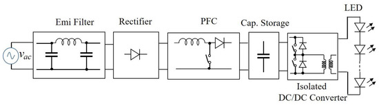
Figure 1.
Block scheme of AC/DC and DC/DC conversion system for high power LED lighting.
In this article, we focused on the impact of the input current ripple in the IBPFC on CCM operation. The current ripple was investigated considering a buck-type equivalent converter as shown in the next sections. The envelope of the peak of current ripple was used to design the inductance values. From Kolar et. al. [14,15], the inductance design was based on the peak-to-peak amplitude of the input current ripple. In calculating the inductance, the ripple amplitude must not exceed the average value of the output current of the single leg of the converter to remain in CCM operation. In the design methodology presented, instead the derivative of the peak of the current, the ripple was used. The critical inductance value was found by comparing the derivative of the input current with the derivative of the peak of the current ripple, as shown in the appropriate section. The methodology presented is an alternative to the solutions proposed by the authors of [14,15] with equally valid results. The article starts with a description of the three-legs IBPFC operation. The design issues of the PFC converter are analyzed. Finally, the experimental evaluation of the described PFC circuit up to 3 kW of rated power is illustrated.
2. Three-Stage Interleaved PFC Converter Operation
In a PFC circuit, the goal is to draw the input current in phase with the input sinusoidal voltage and to arrange for a constant DC output voltage. The input current and input voltage must have a PF very close to unity using a suitable control circuit.
The topology implemented as the PFC circuit is a unidirectional boost converter with IGBTs as switches and fast diodes. In power system applications ≥ 1 kW, several boost converter modules are connected in parallel obtaining an interleaved solution. The boost interleaved PFC increases the power capability and the current ripple variation both in the input and output converter stage [14]. The command signals of the switches are supplied in out of phase mode according to
where Nc is the quantity of legs in the interleaved boost circuit. In the proposed IBPFC application, a three-leg boost is considered to arrange a relatively higher-power circuit optimizing the size of the power devices and reactive components, such as single-stage inductors. The adopted circuit scheme of a three-legs boost converter is depicted in Figure 2a. The power devices are driven by a proper phase-regulator circuit (with the correct phase-shift). In the following analysis, it was supposed that the converter circuit worked in a steady state. Moreover, the converter was in CCM operation. From the classic analysis of the boost converter, one can derive the basic law that links the input voltage vin, the duty cycle of the single controlled switch dsw, and the output voltage vout.
where the on period ton,sw of the controlled switch is equal to
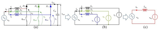
Figure 2.
(a) Three-stage interleaved boost PFC circuit schematic, (b) equivalent averaged-circuit model circuit, (c) Thevenin equivalent circuit.
For the analysis of the current ripple on the input side, it is easier to use the conventions of the buck converter. Moreover, the current ripple (Δipk) does not depend on the average current transferred, but only on the integral of the voltage applied to the inductance.
Based on this choice, the duty cycle D is defined as
where .
In the three-leg arrangement, three diverse operating zones can be recognized in relation of the duty cycle variation [16].
To simplify the analysis, the equivalent circuit adopting the averaged-circuit model of the three phase PFC topology is considered, as depicted in Figure 2b. Considering the input converter stage, the Thevenin equivalent circuit is obtained and described in Figure 2c. The analysis is oriented to know the behavior of the input current, iin. For this reason, the equivalent voltage veq, related to Figure 2c is introduced.
where va, vb, and vc are the voltage across the switches, respectively, qswa, qswb, qswc (Figure 2a).
Considering the equivalent circuit of Figure 2c, an equivalent inductor Leq is also presented:
where L is the single stage inductor (L = La = Lb = Lc of Figure 2a).
The methodology adopted can be extended to n switching cells, considering, respectively:
2.1. D < 1/3 Control Condition
The case of D less than one-third the qualitative waveforms is reported in Figure 3. Figure 3a shows a time spacing of the gate signal commands of the active switches present in the circuital topology. In Figure 3b, the three-leg voltages va, vb, and vc, are reported and compared with the ideal input voltage vin. In Figure 3c, the voltage stimulus veq has a frequency 3.fsw (fsw is the switching frequency) and an amplitude of one-third. The equivalent voltage is in the range of
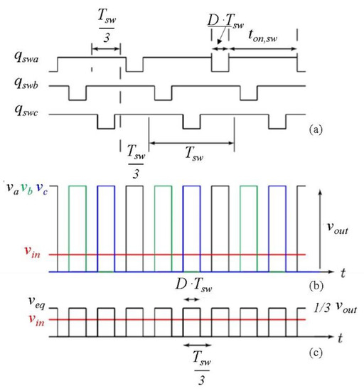
Figure 3.
Switching waveforms behavior in the case of D < 1/3. (a) Gate control signal, (b) single-stage voltage behavior compared with the input voltage vin, (c) equivalent voltage behavior. It shows a frequency 3. fsw compared to the va, vb, and vc voltages, while the amplitude is one-third.
Taking into account the equivalent voltage, it is feasible to compute the variation of the total equivalent magnetic flux related to Figure 2c. It is calculated through the voltage across of the equivalent inductance above mentioned by means of a mathematical integration. In this way, the magnetic flux peak is achieved:
Processing (9), the following is obtained:
In D = 1/6, the maximum peak flux ripple is achieved, from which:
2.2. 1/3 < D < 2/3 Control Condition
Figure 4 shows the generic situation with duty cycle between 1/3 and 2/3. In this case, the equivalent voltage is in the range:
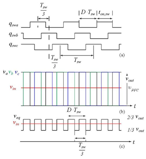
Figure 4.
The qualitative waveforms for 1/3 < D < 2/3. (a) The device control signal, (b) the devices switching voltage, (c) the equivalent voltage behavior.
Using the same computational approach of the previous case, the flux equivalent ripple variation is:
Taking into account the extreme value of the range of veq in Equation (12), the peak of the equivalent flux is given by:
The maximum flux peak occurred for D = ½ and is equal to the value found in Equation (11).
2.3. D > 2/3 Control Condition
Qualitative waveforms in the operative conditions with D > 2/3 are depicted in Figure 5. In this case, the equivalent voltage is in the range:
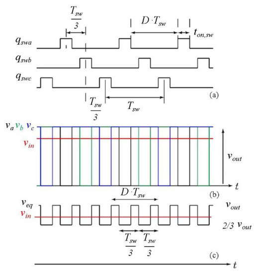
Figure 5.
The qualitative switching waveforms in the case of D > 2/3. (a) The gate signal control, (b) the devices switching voltage, (c) the equivalent voltage variation.
By means the same approach as in the previous cases, the peak flux is obtained as:
The maximum peak for the magnetic flux is obtained with D = 5/6, similarly to Equation (11).
2.4. Converter Behavior within the Whole Operating Range
From Equations (10), (14), and (16), equivalent peak of the flux ripple versus D can be graphed. The input peak of current ripple is:
Assuming a concrete case of study with Tsw = 1/60 kHz, an output voltage vout = 400 V, and a leg inductance L = 900 μH, the ripple curves obtained for the three-leg IBPFC are depicted in Figure 6a (magnetic flux), while the peak of the input current ripple is reported in Figure 6b. The maximum peak value from Equation (11) is Δψpk,eq_max = 92.59 μVs. In Figure 6b, the maximum current peak obtained by Equation (17) is Δipk,Leq = 0.309 A.
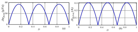
Figure 6.
(a) Ripple of magnetic flux behavior for the three-leg IBPFC, (b) total ripple current behavior. Design parameters fsw = 60 kHz, vout = 400 V and L = 900 μH.
In Figure 6a, three peak points for the flux for the three control conditions with two ripple free points in D = 1/3 and D = 2/3 are observable. The same qualitative considerations can be made for current ripple. It must be noted that the three boost legs are subject to the same stress in terms of ripple, even changing the number of parallel legs. The advantage of paralleling legs consists in reducing the equivalent ripple stress on the grid side and the DC side. The only stress reduction in the single boost legs is represented by the reduction of the processed power by every single leg, which is equivalent to the entire power divided by the number of legs.
The input current ripple is influenced by the factors that shape its variation, such as the output current and both input and output voltage. In specific operating conditions, the current can move from the CCM condition to the Discontinuous Conduction Mode (DCM). The DCM can present control issues, especially with digital controllers. Critical operating conditions are useful for designing the value of the inductor L to maintain the CCM for the interleaved boost converter and therefore avoiding risks of loss of control. In the following section, the same design issues for the actual PFC converter are discussed.
3. Interleaved Boost PFC Design Issues
The design procedure of the Leq inductor starts by considering the PFC in ideal operating conditions. The input voltage is sinusoidal. It is given by
In the ideal case, the input current is
The correct design of the inductor Leq must guarantee that the PFC converter works in CCM within the operating power range. The critical value of the inductance design is related to the worst working conditions. In this case, the DCM operation may be reached. The worst condition occurs at a maximum input voltage, Vin,max at minimum input current Iin,min and maximum current ripple amplitude Ipk,Leq. In the case study considered, the main project constraints are shown in Table 1.

Table 1.
Main inductor design constraints.
The critical inductance computation depends on the input current peak value. To understand the trend of the peak of the current ripple an inductance of Leq = 300 μH is taken into account. From Equation (17), the peak of current ripple can be estimated, as shown in Figure 7. By means of the peak current ripple, the upper and lower envelopes of the actual current flowing in the equivalent inductor can be plotted. The current iup (t) and ilow (t) are given by
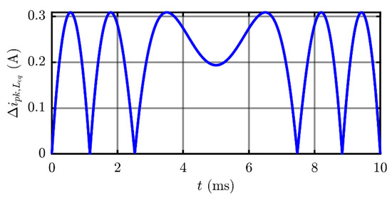
Figure 7.
Current ripple peak behavior in the case of Leq = 300 μH.
During working conditions, the instantaneous current of the inductor was included within the peak ripple envelopes.
By comparing the trend of the input current and the peak of the ripple current flowing in Leq, it is possible to find a design condition to obtain the value of the critical inductance. In Figure 8, the view of the input current and the current peak trended very close to zero in the case of two inductance values Leq = 900 μH, Figure 8a and Leq = 300 μH, Figure 8b at the output power of 400 W. From the inspection of Figure 8, it is observable that as the inductance decreased, the slope of the ipk,Leq increased, becoming greater than the one of the input current. From the observation of the waveforms related to the ilow shown in Figure 9a,b, it can be seen that when the slope of the ripple peak of the current flowing in Leq was greater than the one of the input current, the converter operated in DCM. On the other hand, when the slope of the peak of the ripple of the current is lower than that of the input current, the ilow is always positive, resulting in CCM condition.
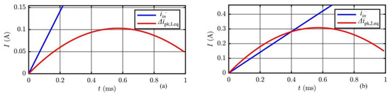
Figure 8.
(a) Peak current ripple and input current comparison for Leq = 900 μH, (b) Peak current ripple and input current comparison for Leq = 300 μH.
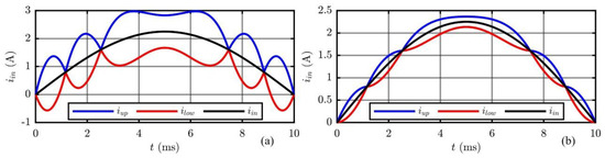
Figure 9.
Input moving average current iin waveform was included within the peak ripple envelopes iup (t) and ilow (t). (a) Current envelopes behavior with Leq = 100 μH, (b) current envelopes behavior with Leq = 500 μH.
To ensure CCM operation, it must be imposed:
From Equation (22), calculating the derivatives at t = 0 of the iin and the ripple peak, ipk,eq flowing in Leq, the boundary condition to work in CCM is obtained:
The mathematical steps to obtain Equation (23) are explained in Appendix A. From the data in Table 1, the critical value of Leq must be greater than 185 μH.
3.1. Output Capacitor Design
Considering a single-phase AC supply, the voltage ripple on the output capacitors of the IBPFC is at two times the grid frequency. It is related also to the pulsed power that moves from input to output of the converter. The dc-link voltage vout is
where Vout is the average of the output voltage, while Δvout is the voltage ripple. Δvout must be selected in order to allow the following constraint:
vout must always be greater than vin,max to maintain the boost voltage conditions and vout must be less than the breakdown of the diodes and power switches of the interleaved legs. Moreover, the required quality of vout must be guaranteed depending on the needs of the cascaded DC/DC converter. The output capacitance Cdc is related to the Δvout and depends on the maximum output power and the twice of angular mains frequency ωin [14].
In this paper, Δvout has been selected equal to 2%, while Pout maximum is 3 kW and Vout = 400 V. Therefore, from (25) the capacitance Cdc,min is equal to 1500 μF.
3.2. Power Devices Selection
The devices selected as switches in the three legs of interleaved PFC topology were trench-gate field-stop IGBTs [17]. The field-stop IGBTs combine no-punch through (NPT) and punch-through (PT) features. The last generation field-stop IGBT show remarkable short-circuit ruggedness. Short-circuit performance is useful to improve the reliability of the IBPFC [18,19]. Moreover, a positive temperature coefficient for high collector current, similar to the MOSFETs, allows an easy parallel connection in high current converter applications [20]. Besides, the IGBTs show a better VCE,sat/Eoff behavior with low Eoff and limited tail in the turn-off current. A silicon IGBT solution is a good tradeoff among ruggedness, cost, power losses, and dynamic characteristics for the selected frequency of 60 kHz compared to silicon MOSFETs super-junction solution [21]. The breakdown voltage is related to the maximum output voltage vout. The current IIGBT,rms at maximum output power of 3 kW in every leg was
where the Vin,min was 10% less than the rated Vin,rms. The IIGBT,max was
The maximum IIGBT,max current at the rated power of 3 kW was about 7.5 A. The devices selected were 20 A, 600 V trench-gate field-stop IGBTs. The diodes had a breakdown voltage related to the maximum voltage vout. The maximum diode current of each leg was
where Vout,min was computed with Equation (24). ID,max, at the rated power of 3 kW, was about 3 A. The selected devices were 12 A, 600 V fast switching silicon diodes.
4. Interleaved Boost PFC Experimental Evaluation
The laboratory converter setup for the experimental tests is shown in Figure 10. In Figure 10a, the electrical scheme is shown. In Figure 10b, a photo of the experimental board during a measurement test is shown. The three-cell IBPFC was controlled by a dedicated controller IC. The controller circuit chosen was a commercial integrated circuit (FAN9673), which allowed us to control the PFC boost up to three interleaved channels in CCM mode. FAN9673 acted through a leading-edge control of the average current. The proper design method of the controller circuit was described by the authors of [22]. It was fully compliant with the IEC61000-3-2 specification.
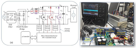
Figure 10.
(a) Interleaved three cells boost interleaved PFC converter set-up with controller circuit. The PFC circuit is linked to a full-bridge diode rectifier, an electronic load to emulate a current constant load is connected to the converter output. (b) Photo of measurement setup.
Furthermore, the controller IC applied a suitable enabling function to the switches. It enabled the number of boost-legs necessary based on the output current demand. At low output current, a single cell was enabled (with the output current less than one-third of the maximum current managed by the controller). Then, the operation of two or three switching stages was enabled in case a larger load must be supplied. The management of the switch-enabling function optimized the IBPFC efficiency.
The microcontroller unit (MCU) used (Figure 10a) was an STM32F446RE from STMicroelectronics. The microcontroller was programmed in C language to emulate the demands of the LED lighting load. In particular, it provides the PFC controller a feedback on the required DC load. In this way, the FAN9673 controller IC knows how to turn on or off the IBPFC legs as the power level changes. The user interface with the MCU was provided by an SPI and CAN communication, which can be used in a later stage for the control of the whole converter system. As shown in the previous section, the interleaved solution produced a remarkable decrease in both input and output currents ripple. The benefits of the ripple act on the conducted EMI filtering size and cost reduction [23]. The correct PCB layout design is a further important issue to mitigate EMI levels of the converter systems. In the actual realization of the experimental prototype, the DC/DC converter and the LED load are emulated by a constant current controlled electronic load. In the experimental prototype, only the IBPFC was investigated. The electronic load allowed us to establish the IBPFC output current based on the number and power required of the LED lighting system to be implemented.
The main PFC electrical parameters in the actual experimental prototype are reported in Table 2. The choice of L = 900 μH for each leg allowed us to obtain a large margin to CCM operative conditions compared with the minimum power rate of 1000 W of the design constraints (Table 1). From Equation (23), it was possible to compute the minimum power boundary in CCM operative conditions for a selected Leq = 300 μH to obtain Pout,min in CCM equal to 1000 W. The experimental switching waveforms at a rated power of Pin = 3000 W in working conditions using all three legs of the PFC boost interleaved are reported in Figure 11. In this operative condition, the main electrical quantities can be extracted from Table 3.
Table 2.
Main PFC electrical parameters of the experimental prototype.
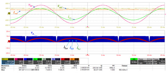
Figure 11.
Switching waveforms of three cells interleaved PFC converter. vin = 100 V/div, iin = 10 A/div, Vout = 200 V/div, Iout = 5 A/div, iLa = iLb = iLc = 5 A/div, va = 200 V/div, Pin = 3 kW, t = 5 ms/div.
Table 3.
Main IBPFC Electrical quantities at a different input power.
The switching waveforms at Pin = 1 kW are reported in Figure 12. In this operative condition, the controller works by making only one leg work. From the inspection of Figure 12, the increase of input current ripple clear appeared, which was compared with the same current waveform depicted in Figure 11.
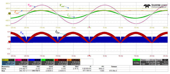
Figure 12.
Switching waveforms of boost PFC converter at Pin = 1 kW with only one working cell. vin = 100 V/div, iin = 10 A/div, Vout = 200 V/div, Iout = 5 A/div, iLa = iLb = iLc = 5 A/div, va = 200 V/div, t = 5 ms/div.
Furthermore, the converter, as shown in Figure 12, worked in CCM condition as estimated in the design constraints. The main electrical quantities, such as the current Total Harmonic Distortion (THD), the power factor, and the efficiency of the PFC, are reported in Table 3 at different input powers. The THD is a significant parameter to control in electronics equipment connected to the grid and it should be maintained at a low value to obtain a quality in main network waveforms. Lower values of THD in power electronic converter applications lead an increasing power factor with lower peak currents. Also, the efficiency can be improved [24]. In Figure 13, the current THD (Figure 13a), the power factor (Figure 13b), and the converter efficiency (Figure 13c) are depicted. The graphs depicted in Figure 13 show, at a glance, the quite satisfactory behavior of the main electrical quantities of the PFC converter. In high-performance LED drivers, THD is efficiently mitigated and is less than 10%. The THD percent in the proposed interleaved boost PFC application was less than 6% in the power range of 1–3 kW. Since the number of operating cells is correlated to the load current demand [25]. The currents in the switches of the PFC changed, as reported in the three different working conditions described in Figure 14.
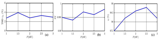
Figure 13.
The graphic behaviors of the current THD (a), the power factor, (b) and the converter efficiency, and (c) of the interleaved three cells PFC front-end converter in the range of 1–3 kW.
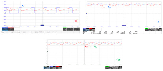
Figure 14.
The inductor current waveforms behaviors of the interleaved cells intervention at load current request variation. (a) Pin = 1 kW, (b) Pin = 2 kW, (c) Pin = 3 kW. iLa = iLb = iLc = 2 A/div, va = 200 V/div, t = 10 s/div.
In Figure 14a, a single-leg PFC worked based on the output of the current requested. The iLa and va waveforms are shown at input power, Pin = 1 kW. In Figure 14b, Pin = 2 kW, in this case, two cells were switched in a suitable phase-shift way. The currents related to leg a (iLa) and leg b (iLb) are reported. Finally, in Figure 14c, three legs operated (Pin = 3kW), and the currents iLa, iLb, and iLc are shown.
5. Discussion
In the high-power LED lighting driver connected to the grid, a PFC converter is a crucial power electronic system in the design of industrial lighting performing equipment. The topological solution of the interleaved boost PFC was used when the power required by the load was higher by paralleling different cells of the converter. Despite the use of the extra legs, there were advantages both in the converter efficiency and size. The frequency of the input and output current ripple is the number of legs multiplied by the switching frequency fSW, thus reducing the required input filter and boost inductors compared to a single leg solution. The design issues of the interleaved boost PFC converter were dealt by deriving the equivalent circuit, where the attention was focused on the transfer function between vin and vout by introducing a duty cycle as the ratio of these two voltages. Looking at the equivalent circuit, a different method was obtained, which allowed us to analyze the dynamics of the electrical quantities related to the equivalent inductance to find an original design criterion of the equivalent inductance which takes into account the envelope of the current ripple. An experimental PFC prototype was implemented, and several tests in the range of 1–3 kW were carried out. The power switches used are the last generation of IGBT devices with fast silicon diodes to realize the three interleaved boost cells with a switching frequency of 60 kHz. A commercial control circuit was applied to achieve a leading-edge average current method. The control circuit implemented a channel management operation. This enabled a different number of legs based on the load current request, optimizing the converter performance and the devices stress. The measured THD, power factor, and efficiency were quite satisfactory, and the PFC converter was a cost-effective solution thanks to use of IGBT devices instead of SIC or super junction MOSFETs.
The next steps were aimed at the engineering of the prototype and the construction of a complete driving system AC/DC (PFC just presented) and DC/DC (constant current converter in developing stage) for high-power density LED lighting systems with high performance and reduced costs.
6. Conclusions
In this article, a flexible three-leg IBPFC converter suitable for high-power LED driver circuit connected to the grid was presented and discussed. The PFC analysis and design were deeply analyzed, defining the constraints and methods of designing passive components, such as the inductors and output capacitor. Moreover, the power devices selection criteria were considered.
An experimental evaluation of the PFC performances in terms of efficiency, power factor, and THD were carried out in the power range of 1–3 kW. A dedicated control circuit IC was considered in the converter prototype implementation, which enabled the correct number of cells depending on the load consumption. The flexible number of cells achieved an optimized converter performance in terms of efficiency and devices stress. The power switches used in the converter application were field-stop trench-gate IGBT devices and fast silicon diode. The power switches choice permitted quite satisfactory performance at a cost-effective solution.
Author Contributions
Conceptualization, S.M. and F.M.; methodology, E.A.; software, E.A. and F.M.; validation, S.B. and S.M.; formal analysis, R.B. and E.A.; investigation, S.M. and E.A.; resources, R.B.; data curation, S.M., F.M. and S.B.; writing—original draft preparation, S.M. and F.M.; writing—review and editing, R.B., E.A. and F.M.; visualization, S.B. and E.A.; supervision, R.B. All authors have read and agreed to the published version of the manuscript.
Funding
The research was funded by the Power Electronics Innovation Center (PEIC) of Politecnico di Torino.
Conflicts of Interest
The authors declare no conflict of interest. The funders had no role in the design of the study; in the collection, analyses, or interpretation of data; in the writing of the manuscript, or in the decision to publish the results.
Appendix A
The CCM operating condition was obtained by imposing Equation (22);
From Equation (19):
Vin,rms is the maximum value of RMS value of vin:
with
The derivative operation of the function takes place around t = 0 for which the time interval was considered:
where
In t = 0:
From Equation (22);
By processing Equation (A10), Equation (23) was obtained. The minimum output power to work in CCM was obtained from Equation (23):
where
References
- Chen, M.; Lin, S.; Chou, D.; Chen, J. Study of driving source efficiency improvement for high power LED street lighting system using Taguchi method. In Proceedings of the 2016 IEEE International Conference on Industrial Technology (ICIT), Taipei, Taiwan, 14–17 March 2016; pp. 372–377. [Google Scholar]
- Lee, S.; Choe, H.; Yun, J. Performance Improvement of a Boost LED Driver with High Voltage Gain for Edge-Lit LED Backlights. IEEE Trans. Circuits Syst. II Express Briefs 2018, 65, 481–485. [Google Scholar] [CrossRef]
- di Mauro, S.; Musumeci, S.; Raciti, A. Analysis of electrical and photometric quantities of CFL and LED bulb lamps. In Proceedings of the 2017 IEEE Industry Applications Society Annual Meeting, Cincinnati, OH, USA, 1–5 October 2017; pp. 1–8. [Google Scholar]
- Raciti, A.; Rizzo, S.A.; Susinni, G. Steady-State Electrical Modeling of LED and CF Bulb Lamps Under Variable Voltage on the Main. In Proceedings of the 2018 IEEE International Conference on Environment and Electrical Engineering and 2018 IEEE Industrial and Commercial Power Systems Europe (EEEIC/I&CPS Europe), Palermo, Italy, 12–15 June 2018; pp. 1–6. [Google Scholar]
- Liu, Z.; Lee, H. A Current-Accuracy-Enhanced Wide-Input-Range DC–DC LED Driver with Feedforward Synchronous Current Control. IEEE Trans. Circuits Syst. I Regul. Pap. 2018, 65, 3996–4006. [Google Scholar] [CrossRef]
- Chen, W.; Cheng, K.W.E.; Shao, J. Circuit Topology Analysis for LED Lighting and its Formulation Development. Energies 2019, 12, 4203. [Google Scholar] [CrossRef]
- Kalla, U.K. A PFC based control scheme for LED lighting systems. In Proceedings of the 2016 IEEE 7th Power India International Conference (PIICON), Rajasthan, India, 25–27 November 2016; pp. 1–4. [Google Scholar]
- Raciti, S.; Rizzo, A.; Susinni, G. Parametric PSpice Circuit of Energy Saving Lamp Emulating Current Waveform. Appl. Sci. 2019, 9, 152. [Google Scholar] [CrossRef]
- Balogh, L.; Redl, R. Power-factor correction with interleaved boost converters in continuous-inductor-current mode. In Proceedings of the Eighth Annual Applied Power Electronics Conference and Exposition, San Diego, CA, USA, 7–11 March 1993; pp. 168–174. [Google Scholar]
- Raggl, K.; Nussbaumer, T.; Doerig, G.; Biela, J.; Kolar, J.W. Comprehensive Design and Optimization of a High-Power-Density Single-Phase Boost PFC. IEEE Trans. Ind. Electron. 2009, 56, 2574–2587. [Google Scholar] [CrossRef]
- Liu, J.; Chen, W.; Zhang, J.; Xu, D.; Lee, F.C. Evaluation of power losses in different CCM mode single-phase boost PFC converters via a simulation tool. In Conference Record of the 2001 IEEE Industry Applications Conference, Proceedings of the 36th IAS Annual Meeting (Cat. No.01CH37248), Chicago, IL, USA, 30 September–4 October 2001; Institute of Electrical and Electronics Engineers: Piscataway, NJ, USA, 2001; Volume 4, pp. 2455–2459. [Google Scholar]
- Borlo, S.; Cittanti, D.; Gregorio, M.; Mandrile, F.; Musumeci, S. Comparative CCM-DCM Design Evaluation of Power Inductors in Interleaved PFC Stage for Electric Vehicle Battery Chargers. In Proceedings of the 2019 International Conference on Clean Electrical Power (ICCEP), Otranto, Italy, 2–4 July 2019; pp. 180–186. [Google Scholar]
- Kong, P.; Wang, S.; Lee, F.C.; Wang, C. Common Mode EMI Study and Reduction Technique for the Interleaved Multichannel PFC Converter. IEEE Trans. Power Electron. 2008, 23, 2576–2584. [Google Scholar] [CrossRef]
- Nussbaumer, T.; Raggl, K.; Kolar, J.W. Design Guidelines for Interleaved Single-Phase Boost PFC Circuits. IEEE Trans. Ind. Electron. 2009, 56, 2559–2573. [Google Scholar] [CrossRef]
- Biela, J.; Kolar, J.W.; Deboy, G. Optimal design of a compact 99.3% efficient single-phase PFC rectifier. In Proceedings of the 2010 Twenty-Fifth Annual IEEE Applied Power Electronics Conference and Exposition (APEC), Palm Springs, CA, USA, 21–25 February 2010; pp. 1397–1404. [Google Scholar]
- Messina, S.; Torrisi, M.; Cacciato, M. Three-channels interleaved PFC exploiting mixed signal control. In Proceedings of the 2017 19th European Conference on Power Electronics and Applications (EPE’17 ECCE Europe), Warsaw, Poland, 11–14 September 2017; pp. P.1–P.10. [Google Scholar]
- Alessandria, A.; Fragapane, L.; Morale, G. Design considerations on Field-Stop Layer processing in a trench-gate IGBT. In Proceedings of the 2009 13th European Conference on Power Electronics and Applications, Barcelona, Spain, 8–10 September 2009; pp. 1–6. [Google Scholar]
- Cristaldi, D.; Musumeci, S.; Raciti, A. Modelling and Simulation of IGBT Thermal Behavior During a Short Circuit Power Pulse. In Proceedings of the International Conference on Clean Electrical Power, 2015 IEEE, ICCEP 15, Taormina, Italy, 16–18 June 2015; pp. 542–547. [Google Scholar]
- Musumeci, S.; Pagano, R.; Raciti, A.; Frisina, F.; Melito, M. Transient behavior of IGBTs submitted to fault under load conditions. In Proceedings of the 2002 IEEE Industry Applications Conference. 37th IAS Annual Meeting (Cat. No.02CH37344), Pittsburgh, PA, USA, 13–18 October 2002; Volume 3, pp. 2182–2189. [Google Scholar]
- Raciti, A.; Musumeci, S.; Xibilia, F.; Chimento, F.; Privitera, G. A bi-dimensional model for power MOSFET devices accounting for the behavior in unclamped inductive switching conditions. In Proceedings of the IECON 2013—39th Annual Conference of the IEEE Industrial Electronics Society, Vienna, Austria, 10–13 November 2013; pp. 134–139. [Google Scholar]
- Musumeci, S.; Cristaldi, D.; Portoghese, F. Super-junction power MOSFET in half bridge DC-DC zero-voltage converter for energy conversion management. In Proceedings of the 2015 International Conference on Clean Electrical Power (ICCEP), Taormina, Italy, 16–18 June 2015; pp. 755–760. [Google Scholar]
- Cheng, L.; Kai, Y.; Xiaoguang, W.; Dezhang, L. A design of single phase inverter with three-channel interleaved PFC module. In Proceedings of the 19th International Conference on Electrical Machines and Systems, ICEMS 2016, Chiba, Japan, 13–16 November 2016; pp. 1L–5L. [Google Scholar]
- Kolar, J.W.; Drofenik, U.; Minibock, J.; Ertl, H. A new concept for minimizing high-frequency common-mode EMI of three-phase PWM rectifier systems keeping high utilization of the output voltage. In Proceedings of the PEC 2000. Fifteenth Annual IEEE Applied Power Electronics Conference and Exposition), New Orleans, LA, USA, 6–10 February 2000; Volume 1, pp. 519–527. [Google Scholar]
- Jiang, C.; Nene, H.; Choudhury, S. Efficiency and THD Optimization Based on an Interleaved PFC Converter Using Digital Controller with Integrated Valley Switching Control Feature. In Proceedings of the 2019 IEEE Texas Power and Energy Conference (TPEC), College Station, TX, USA, 7–8 February 2019; pp. 1–5. [Google Scholar]
- Musumeci, S.; Bojoi, R.; Borlo, S.; Armando, E. IGBT based Three Channel Interleaved PFC Boost Converter for Inverter Front-End Application. In Proceedings of the 2019 AEIT International Annual Conference (AEIT), Florence, Italy, 18–20 September 2019; pp. 1–6. [Google Scholar]


© 2020 by the authors. Licensee MDPI, Basel, Switzerland. This article is an open access article distributed under the terms and conditions of the Creative Commons Attribution (CC BY) license (http://creativecommons.org/licenses/by/4.0/).