Abstract
The output LC filter of a photovoltaic (PV) string three-level grid-tied inverter that connects the filter capacitor neutral point to dc-link capacitor neutral point can reduce the common-mode (CM) current injected to the grid by letting the CM current circulate within the inverter. However, the internal CM current may resonate because of the existence of the resonant frequency of the internal CM LC circuit. Compared with the traditional continuous pulse-width modulation (CPWM), the resonance can be worse if discontinuous pulse-width modulation (DPWM) is applied, for the zero sequence quantity of DPWM contains more harmonics than that of CPWM. In this paper, a virtual negative resistor based common mode current resonance suppression method for a three-level grid-tied inverter is proposed to overcome the CM current resonance problem in DPWM application. Different positions of the virtual negative resistor in the equivalent CM circuit with different feedback variables are analyzed theoretically. The virtual negative resistor connected in series with the inductor in the equivalent CM circuit is selected to damp the CM current resonance for simplification and damping performance. Different from the implementation in CPWM where a pair of small voltage vectors exist and are used to adjust the CM voltage directly, the proposed method for DPWM application is implemented indirectly by adding the CM adjustment quantity to differential-mode (DM) control quantity with appropriate coefficients. Depending on the sector of DM control quantity in the
reference frame, the coefficients are calculated using one of three specific voltage vectors. Experimental results are given to demonstrate the effectiveness of theoretical analyses and the proposed method.
1. Introduction
Among all renewable energy sources, photovoltaic (PV) systems have experienced rapid growth both in residential and commercial applications. The power quality of current generated by the PV grid-connected inverter is of importance for the grid. According to IEEE Std 519-2014, the recommended harmonic distortion limit of line-to-neutral voltages is that the voltage total harmonic distortion (VTHD) at the point of common coupling (PCC) is 8% for the bus voltage less than or equal to 1 kV, 5% for the bus voltage between 1 and 69 kV, 2.5% for the bus voltage between 69 and 161 kV, etc., [1]. Switching ripple filters (SRFs), like L, LC, LCL, and LLCL filter, is a significant part of PV grid-connected inverter interfacing with the grid. On one hand, SRFs can maintain a coupling connection and integration between grid and grid-connected inverter. On the other hand, SRFs can filter the switching ripple currents of inverter-side inductor current [2]. However, these filters can potentially cause a harmonic resonance for system operation if not properly designed [3].
In order to suppress the harmonic resonance problems, researchers have proposed passive damping (PD) and active damping (AD) techniques [3,4,5]. PD is a simple and stable technique but increases the damping power loss and volume of an inverter. Compared with PD, AD technique is flexible and does not increase the damping power loss. The three most cited AD techniques in literature are capacitor current feedback based method [6], capacitor voltage feedback based method [7], and notch-filter based method [8]. Different feedback of output filter state corresponds to different impedance position in a LCL filter: the feedback of the converter current forms a virtual impedance in series with the inverter side inductor Lf, capacitor voltage, or current feedback in grid current control forms a virtual impedance in parallel with filter capacitor, grid current feedback forms a virtual impedance in parallel with grid side inductor [9]. In [10], the authors give a comprehensive study of a virtual resistor based AD for the LCL resonance frequency. The virtual resistor based AD technique is simple and effective in damping the LCL resonance current. However, to the best knowledge of the authors, the virtual resistor mentioned above is used only for damping the harmonics resonance of differential-mode (DM) current injected to the grid.
An improved LCL (ILCL) filter is proposed in [11,12] to reduce the leakage current. The ILCL filter is acquired simply by connecting the common point of LCL filter capacitors to the dc-link neutral point without adding any additional components. Letting the common-mode (CM) current circuiting within the inverter, the leakage current injected into the grid can be reduced significantly. However, the CM current circuiting path within the inverter is a LC circuit, in which a LC resonance frequency fr exists. The CM current resonance suppression methods for inverter using the ILCL filter are proposed in [13,14] to reduce the leakage current injected to gird. In [14], the authors use a PI controller to control the CM current to be zero by real-time adjusting zero-sequence duty ratio in space vector modulation (SVM) technique. In [13], the CM voltage which is injected into DM voltage to extend the inverter modulation index is controlled to suppression CM current resonance. Both the methods are useful and effective, and are based on a pair of small voltage vectors to adjust the CM voltage.
In order to improve the switching efficiency of three-phase rectifier/inverter, discontinuous pulse-width modulation (DPWM) is proposed by researchers [15,16]. The basic idea of DPWM is to select appropriate voltage vectors to compose the reference voltage vector so that the switches have a minimum switching loss. One of its characteristics is that there is no a pair of small voltage vectors, only one of the two small voltage vectors is used to compose the reference voltage vector. Since the CM AD methods in [13,14] are based on a pair of small voltage vectors to adjust the CM voltage, they cannot be used directly in DPWM application.
In this paper, a virtual negative resistor based AD (VNRBAD) method is proposed to damp the CM current resonance for a three-level inverter with an improved LC (ILC) filter in DPWM application. The originality lies in two points: (1) a virtual negative resistor based CM current resonance suppression method and (2) its implementation in DPWM application.
This work is organized as follows. The model of CM current resonance in three-level grid-tied inverter with an ILC filter is presented in Section 2. In Section 3, the comparison of the harmonics of the zero sequence of DPWM and continuous pulse-width modulation (CPWM) is presented. VNRBAD for CM current resonance suppression in DPWM application is proposed in Section 4. Experiments and discussions are given in Section 5 to demonstrate the proposed VNRBAD. In Section 6, conclusions are reached.
2. Model of CM Current Resonance in Grid-Tied Inverter with ILC Filter
Figure 1 shows the topology of a general PV string three-level grid-tied inverter with an ILC filter [12,17]. Boost converter is usually used as the DC-DC stage to increase the dc voltage and to track the maximum power point of the PV array, the inverter stage is used to convert DC power into AC power and inject it to AC grid. iCM and vCM is the CM LC circuit current and voltage respectively, and is defined by Equations (1) and (2). Detailed modeling derivation of CM voltage and current of the topology can be found in [14]. Here, only the CM circuit model is given in Figure 2. Its transfer function Gp and bode diagram is given in Equation (3) and Figure 3, respectively. The CM resonance frequency in the bode diagram is given in Equation (4). The CM current resonance would be excited in the CM current path if no CM current resonance suppression technique is applied. Such resonance current would be more serious when DPWM is used as the modulation algorithm of PV string inverter, which is explained next.
where, iCM and vCM are the CM current and voltage, ia, ib, ic are three-phase inductor current, respectively. vAo, vBo, and vCo are three-phase bridge output voltage. Gp and fr are the model and the resonant frequency of the equivalent CM circuit, respectively. Lf and Cf are the inductance and capacitance of LC filter. S is a complex variable in S domain, and S = , f is the frequency of current and voltage.

Figure 1.
Grid-connected transformer less three-level I-type inverter with ILC filter.
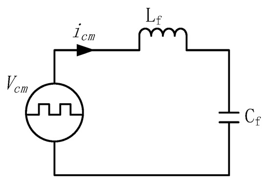
Figure 2.
Common-mode (CM) voltage and current equivalent circuit for three-level inverter with ILC filter, without Cpv considered.
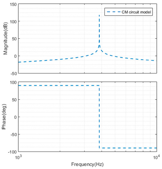
Figure 3.
Bode diagram of CM LC circuit.
3. Harmonics Comparison of Zero Sequence Quantity of DPWM and CPWM
The symmetrical PWM [18,19] is used as CPWM in this paper. The zero sequence quantity of symmetrical PWM is given by Equation (5). A detailed description of DPWM used in this paper can be found in [16]. The zero sequence quantity of DPWM used in this paper is given by Equations (6) and (7) [20]. DPWM is widely used in the PV string inverter for its higher efficiency than that of CPWM.
where Vz is zero sequence quantity, Vx is three-phase voltage, is the intermediate variable, x = a, b, c. is the voltage among which have maximum absolute value. (a mod b) delivers the remainder of the division a/b.
The zero sequence quantity of CPWM and DPWM according to different modulation index and time are shown in Figure 4a,c, respectively. Using discrete Fourier transform, the harmonics comparison of zero sequence quantity between CPWM and DPWM are shown in Figure 4b,d respectively, which shows that the zero sequence quantity of DPWM contains more harmonics than that of CPWM. Hence, the zero sequence quantity of DPWM can lead to more serious CM current resonance than that of CPWM. As is shown in Figure 5, when the modulation method is changed from DPWM to CPWM, the resonance of CM current in io is alleviated.
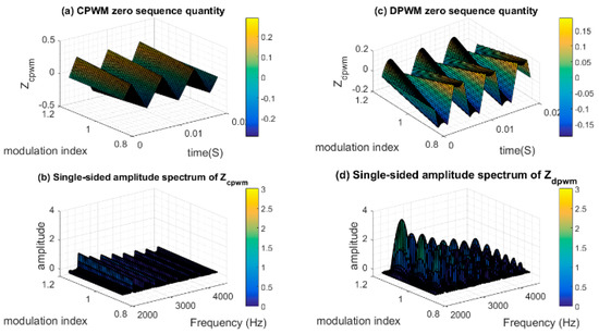
Figure 4.
Harmonics comparison between continuous pulse-width modulation (CPWM) and discontinuous pulse-width modulation (DPWM). (a) CPWM zero sequence quantity. (b) PPWM zero sequence quantity. (c) Single-sided amplitude spectrum of ZCPWM. (d) Single-sided amplitude spectrum of ZDPWM.
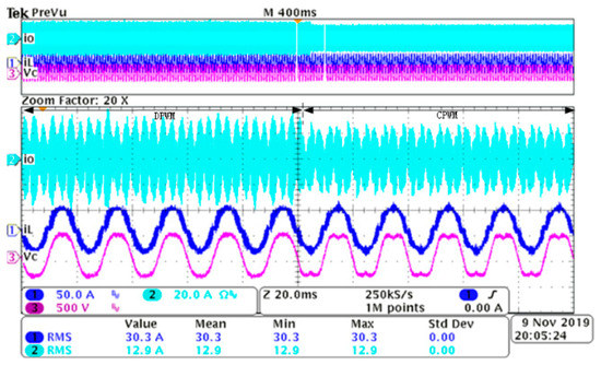
Figure 5.
CM current resonance comparison between CPWM and DPWM at 30A iL.
4. The Proposed VNRBAD Method for CM Current Resonance
4.1. VNRBAD for CM Current Resonance
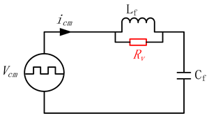
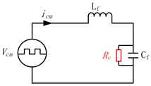
In order to suppress the CM current resonance, VNRBAD is proposed in this subsection. Using the same method as in [10], a general block diagram of the equivalent CM current power stage is proposed, as is shown in Figure 6. Although the same method as in [10] is used, it should be noticed that the analysis equivalent circuit are the major difference: model in [10] is for and only for DM circuit and DM current resonance damping, model in this paper focus on CM circuit and CM current resonance damping. Gad is a VNRBAD controller and is given by Equation (8). Gt is the transfer function from iCM to inductor current iL, capacitor current ic, or capacitor voltage vc, and is given by Equation (9). The virtual negative resistor has three positions in the modified equivalent CM circuit, and the feedback variable can be iL, ic or vc. The modified power stage and its corresponding Gad is given in Table 1 without considering the delay effects.
where, Gp is the power stage circuit transfer function, Gpm is the modified power stage circuit transfer function, Gt is the transfer function from iCM to iL, ic or vc.
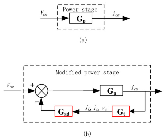
Figure 6.
Block diagram of CM power stage. (a) Power stage, (b) modified power stage.

Table 1.
Different forms of Gad(s) with different filter state variables for active damping (AD).
Using the parameters in Table 2, the bode diagram comparison between the original equivalent power stage and the three modified equivalent power stages are given in Figure 7, Figure 8 and Figure 9, respectively. From these bode diagrams, it can be seen that the virtual negative resistor connected in series with the inductor has the best AD performance. Once the connection type of virtual negative resistor is selected, Gad = Rv is selected from Table 1 for simple implementation purposes.

Table 2.
Photovoltaic (PV) string inverter parameters.
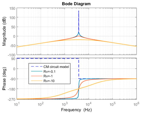
Figure 7.
Bode diagram of CM power stage: without Rv and with Rv connected in series with Lf.
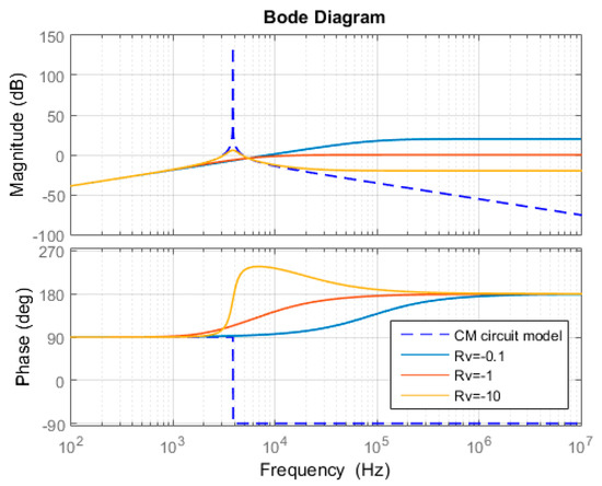
Figure 8.
Bode diagram CM power stage: without Rv and with Rv connected in parallel with Lf.
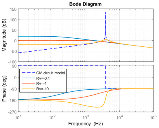
Figure 9.
Bode diagram CM power stage: without Rv and with Rv connected in parallel with Cf.
The virtual negative resistor connected in series with the inductor and Gad = Rv is applied in this paper. The 1.5 times sample period Ts delay is considered, and is given in Equation (10) which composed of computational and PWM delays in the digital control [10]. Since only the harmonics at CM resonance frequency fr is the harmonics needed to damp and usually it is high-order harmonics, the high pass filter (HPF) is applied to cut off the low frequency harmonics in iCM, and is given in Equation (11). The cutoff frequency fc can be chosen as a frequency which lower than fr. In this paper, fr is higher than 2000 Hz, and 1000 Hz is used as fc. The CM current resonance AD control loop with delay and HPF considered is shown in Figure 10. Its bode diagram with different virtual negative resistor values is shown in Figure 11, which shows that the admittance at resonance frequency can be effectively damped with a proper Rv.
where, Ts is the sample period, fc is the cutoff frequency of the first order high pass filter.

Figure 10.
Common mode current suppression control loop.
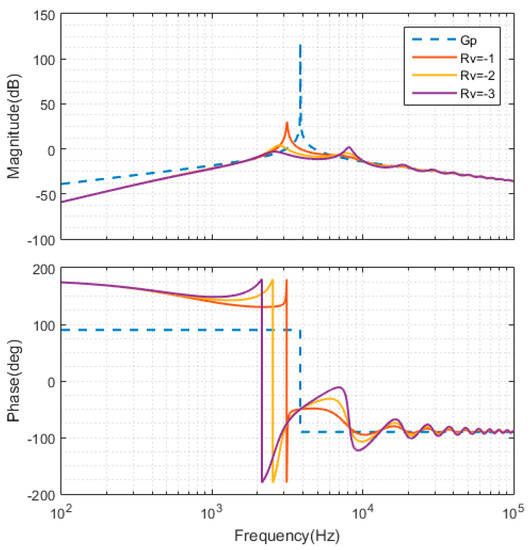
Figure 11.
iL or ic feedback based virtual negative resistor with delay considered.
4.2. The Implementation of VNRBAD for DPWM Application
In [14], the output of CM current controller dCM is added into three final modulation quantities in CPWM application, as is shown in Figure 12 and Equation (12). However, it cannot be used in DPWM application. For example, if phase A is clamped to positive bus voltage, ma is clamped to 1, and dz can be arrived in Equation (13). Substituting Equation (13) into Equation (12), the final three modulation quantity ma, mb, mc can be calculated in Equation (14). From Equation (14), it can be seen that dCM have no effects on ma, mb, and mc, which means the dCM cannot be added directly into three final modulation quantities in DPWM application.
where, ma, mb, mc are three final modulation quantities, respectively; dDMa, dDMb, dDMc are three-phase components of DM current controller outputs; dCM is the CM Rv outputs, dz is the zero sequence quantity of DPWM.

Figure 12.
dCM implementation in CPWM application [14].
The implementation of the proposed method for DPWM application is indirect. Figure 13 show the voltage space vectors in the reference frame for a three-level inverter. Based on voltage vector synthesis principle, once a reference DM voltage vector Vref in sector I in the reference frame is given as a constant voltage vector, the dwell times t1, t11 and t01 will be known constant quantities, as is shown in Equation (15) when using CPWM and in Equation (16) when using DPWM. Similarly, the CM voltage VCM_cpwm using CPWM and VCM_dpwm using DPWM is acquired in Equations (17) and (18). From Equation (17), it can be seen that VCM_cpwm can be controlled by adjusting the distribution factor k without needing to adjust dwell times t1, t11 and t01, which means that there is no coupling relationship between VCM_cpwm and Vref. In CPWM application, DM duty cycle which controls inductor DM current and CM duty cycle which controls inductor CM current are decoupled by a pair of small voltage vectors. In this example, the small voltage vectors are V01_POO and V01_ONN.
where, Vref is the DM voltage vector in the reference frame, VCM_cpwm and VCM_dpwm are the CM voltage when using CPWM and DPWM respectively. Ts is the switching period, Ts = t1 + t11 + t01. t1, t11, and t01 are the dwell time of voltage vector V1, V11, and V01 in Figure 13, respectively. V01_ONN and V01_POO are a pair of small vectors V01. k is the distribution factor for V01_ONN and V01_POO, and 0 < k < 1.
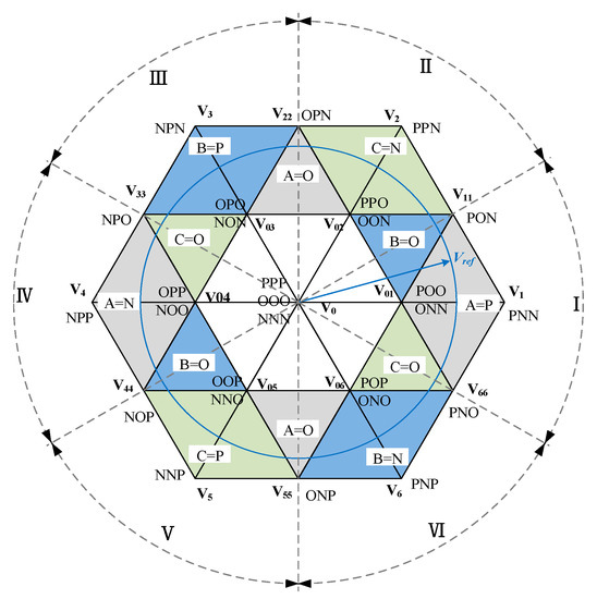
Figure 13.
Voltage space vectors for three-level inverter.
In DPWM application, however, there is no a pair of small voltage vectors. According to Equation (16), if Vref is a given vector, then t1, t11, and t01 are known constant quantities. According to Equation (18), if t1, t11, and t01 are known constant quantities, VCM_dpwm will be a constant quantity, which means that there is a coupling relationship between VCM_dpwm and Vref by dwell time t1 and t01. The only way to control VCM_dpwm is to adjust t1 and t01, which means that VCM_dpwm can only be controlled by adjusting Vref. Vref can be adjusted by compensating one of the three specific compensating vector Vcpi (i = A,B,C). The three specific compensating voltage vectors are shown in Figure 14a. As is shown in Figure 14b, when phase A is clamped to positive bus voltage, the vector VcpA can be used to compensate Vref to increase the dwell time t1 of voltage vector V1 in Equation (18) [21], which can decrease VCM_dpwm. In Figure 14c, Vref is clamped to bus neutral point O. By compensating Vref with VcpA, the dwell time of voltage vector V03 is decreased, which can decrease VCM_dpwm. Similarly, when phase A is clamped to negative bus voltage, the vector VcpA can be used to compensated Vref to decrease the dwell time of voltage vector V4, which can decrease VCM_dpwm. To sum up, when phase A is clamped to DC bus positive, negative, or neutral point voltage, the vector VcpA can be used to compensated Vref to decrease VCM_dpwm.
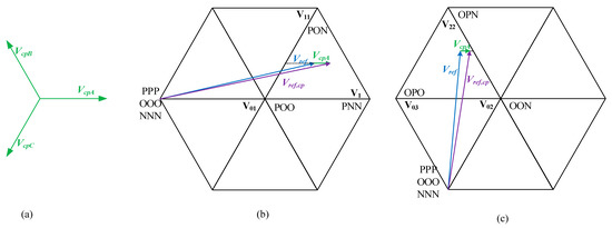
Figure 14.
(a) Three compensation vectors for phase A,B,C; (b)Vref compensation when phase A is clamped to positive bus voltage; (c) Vref compensation when phase A is clamped to bus neutral point O.
Similar analysis can be implemented when phase B,C is clamped to DC bus positive, negative, or neutral point voltage. It can be arrived that VCM_dpwm can be decreased by compensating Vref with Vcpi (i = A,B,C) when phase i (i = A,B,C) is clamped to bus positive, negative, or neutral point voltage.
Vref compensation is implemented in an abc reference frame. As is given in Equation (19), the compensating voltage vector Vcpi (i = A,B,C) in reference frame can be converted to three-phase components dCM_DMa, dCM_DMb, dCM_DMc in the abc reference frame using inverse Clarke transform seen in Equation (20). dCM is the output CM voltage of Rv and determine the amplitude and sign of Vcpi (i = A,B,C). Kfa, Kfb, Kfc are coefficients which determine the angle of Vcpi (i = A,B,C). As is given in Equation (21), Kfa, Kfb, and Kfc is a value chosen from 1, −0.5, and −0.5 for simplification purposes. The value 1 is for the phase which is clamped to bus positive, negative, or neutral point voltage. The value −0.5 is for the remaining two phases. The judgment of clamped phase is based on sector detection algorithm in [21] and DPWM method in [16]. The final three-phase modulation quantities are given in Equation (22). The implementation diagram of VNRBAD for DPWM application is given in Figure 15.
where, dCM_DMa, dCM_DMa, dCM_DMa are the CM adjust quantity added to dDMa, dDMb, and dDMc, respectively. Kfa, Kfb, Kfc is the coefficient which transfers dCM into three DM quantity dDMa dDMb, and dDMc, respectively.
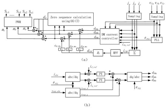
Figure 15.
(a) The implementation of virtual negative resistor based AD (VNRBAD) for DPWM application. (b) The DM current controller.
5. Experiments and Discussion
In order to verify the effectiveness of the proposed VNRBAD method, experiments are implemented in a string inverter produced by TBEA Xi’an Electric Technology Co., Ltd. Grid simulators are used as load and PV simulators are used as DC power supply in the experiment. The specification of the inverter and experiment conditions are given in Table 2. Note that the inductance value of Lf is variable with current conducting through it. The value of 95 μH is a measurement value of Lf at 80A. The model number of devices used in the experiment are shown in Table 3.

Table 3.
Model number of devices used in the experiment.
5.1. The Value of Rv
As is shown in Figure 11, the smaller Rv value it is, the better CM current resonance suppression performance it is. However, Rv cannot be too small for better CM current resonance suppression, because it will degrade DM current injected to grid. Since the CM voltage is controlled by compensating DM voltage, the CM current resonance will be suppressed better when Rv is smaller, while the DM current will be overcompensated and is degraded. As is shown in Figure 16, when Rv is changed from −3 to −1.5, the CM current in io is worse, while the inductor current iL and grid current ig are better. Although the damp performance of io is better when Rv = −3, an apparent current distortion can be observed in iL and ig, which is because the amplitude of the compensated vector is too big. There must be a compromise between the damping performance of io and THD of ig.
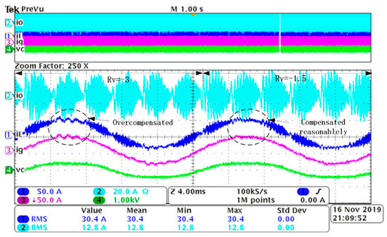
Figure 16.
Waveform of io, iL, ig, and vc with Rv varied from −3 to −1.5.
In practical application, there exist delays in the control loop which will degrade the CM current resonance suppression performance, so it is suggested that the value of Rv can be adjusted from −3 to 0 by hand.
5.2. Comparison between VNRBAD and Without VNRBAD under Different iL
Based on the analysis of Rv above, −2 is chosen as the value of Rv in the experiments. The waveform comparison of io, iL, ig, and vc between VNRBAD and without VNRBAD under different values of iL is given in Figure 17 and Figure 18, respectively. Note that the CM current in iL resonates heavily under 80A iL when without VNRBAD, and the protection program of the control system is triggered to shut down the inverter. The proposed VNRBAD can suppress the CM current resonance effectively, although not completely. The harmonics of iL is shown in Figure 19 and Figure 20, respectively. The harmonics at CM resonance frequency is reduced effectively.
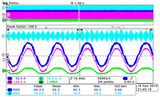
Figure 17.
Waveform comparison of io, iL, ig, and vc between AD and without AD under 60A iL.
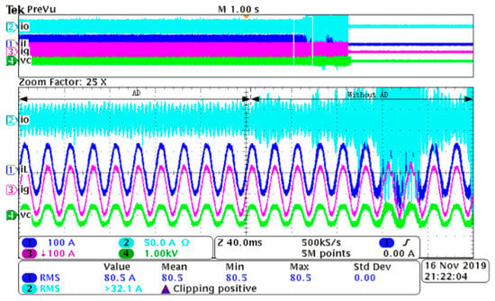
Figure 18.
Waveform comparison of io, iL, ig, and vc between AD and without AD under 80A iL.
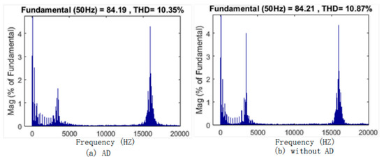
Figure 19.
Harmonics comparison of iL between AD and without AD at 60A iL.
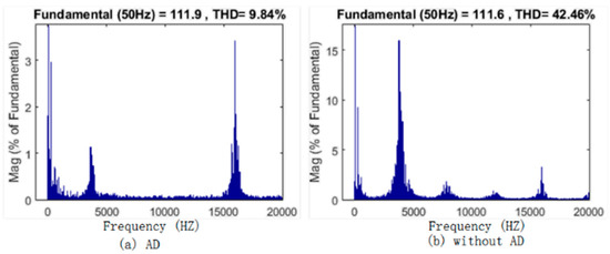
Figure 20.
Harmonics comparison of iL between AD and without AD at 80A iL.
5.3. Discussion
The PD method with a 0.61 ohm resistor connected in series with the inductor in the CM circuit is also implemented. The waveform of io, iL, and ig using PD method is shown in Figure 21. The RMS value comparison of io of three methods under different iL is shown in Figure 22. It can be seen that PD has a better CM current suppression performance compared with the proposed VNRBAD method.
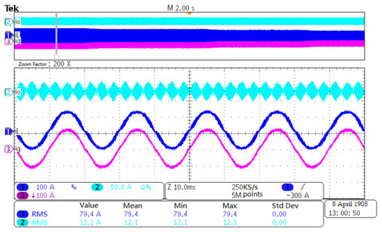
Figure 21.
Waveform of io, iL, and ig under 80A iL using PD.
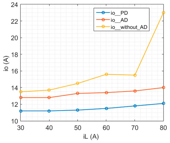
Figure 22.
RMS value of io of three methods under different iL.
Two reasons limit the CM resonance suppression performance of the proposed VNRBAD. One is that there is a compromise between the CM current control performance and DM current control performance. If Rv is too small, the CM resonance current damping performance is not good. On the contrary, too small values of Rv overcompensate DM voltage Vref in reference frame and degrade the quality of DM current ig. Another reason is the delay in the control loop which can be studied further. Although the damping performance of the proposed VNRBAD method is not as good as PD, VNRBAD can suppress the CM current resonance within an acceptable range to let the inverter operate normally in DPWM application.
6. Conclusions
In this paper, VNRBAD is proposed to suppress the CM current resonance for a three-level grid-tied inverter with DPWM. The harmonics comparison of zero sequence quantity between DPWM and CPWM is presented, which shows DPWM has more harmonics than that of CPWM. In DPWM application, the CM voltage and DM voltage is coupled. VNRBAD is implemented by compensating the DM voltage to control the CM voltage. Experimental results demonstrate the effectiveness of VNRBAD. Although VNRBAD is not as good as PD in the experiments, VNRBAD can suppress the CM current resonance within an acceptable range and does not need additional PD power resistor. Future work will focus on the reduction of the delay in the control loop which can enhance the CM current resonance suppression performance of the proposed VNRBAD method.
Author Contributions
S.Z. provided guidance and supervision. Q.L., H.Z., J.Z., and J.L. implemented the main research, performed the experiment, wrote the paper, and revised the manuscript as well. All authors have equally contributed to the theoretical analysis, experiment, and result discussions. All authors have read and agreed to the published version of the manuscript.
Funding
This work was funded by the National Natural Science Foundation of China, Grant No. 51675414, and by the National Natural Science Foundation of China, Grant No. 51907160.
Acknowledgments
The authors would like to thank TBEA Xi’an Electric Technology Co., Ltd for the implementation of the experiments.
Conflicts of Interest
The authors declare no conflict of interest.
References
- IEEE. Recommended Practice and Requirements for Harmonic Control. In Electric Power Systems; IEEE: Piscataway, NJ, USA, 2014; pp. 1–29. [Google Scholar]
- Büyük, M.; Tan, A.; Tümay, M.; Bayındır, K.Ç. Topologies, generalized designs, passive and active damping methods of switching ripple filters for voltage source inverter: A comprehensive review. Renew. Sustain. Energy Rev. 2016, 62, 46–69. [Google Scholar] [CrossRef]
- Liang, X.; Karim, C.A.B. Harmonics and Mitigation Techniques Through Advanced Control in Grid-Connected Renewable Energy Sources: A Review. IEEE Trans. Ind. Appl. 2018, 54, 3100–3111. [Google Scholar] [CrossRef]
- Gomes, C.C.; Cupertino, A.F.; Pereira, H.A. Damping techniques for grid-connected voltage source converters based on LCL filter: An overview. Renew. Sustain. Energy Rev. 2018, 81, 116–135. [Google Scholar] [CrossRef]
- Wu, W.; Liu, Y.; He, Y.; Chung, H.S.; Liserre, M.; Blaabjerg, F. Damping Methods for Resonances Caused by LCL-Filter-Based Current-Controlled Grid-Tied Power Inverters: An Overview. IEEE Trans. Ind. Electron. 2017, 64, 7402–7413. [Google Scholar] [CrossRef]
- Erika, T.; Holmes, D.G. Grid current regulation of a three-phase voltage source inverter with an LCL input filter. IEEE Trans. Power Electron. 2003, 18, 888–895. [Google Scholar] [CrossRef]
- Liserre, M.; Dell’Aquila, A.; Blaabjerg, F. Stability improvements of an LCL-filter based three-phase active rectifier. In Proceedings of the 2002 IEEE 33rd Annual IEEE Power Electronics Specialists Conference Proceedings (Cat No02CH37289), Cairns, QLD, Australia, 23–27 June 2002; Volume 3, pp. 1195–1201. [Google Scholar]
- Dannehl, J.; Liserre, M.; Fuchs, F.W. Filter-Based Active Damping of Voltage Source Converters With $LCL$ Filter. IEEE Trans. Ind. Electron. 2011, 58, 3623–3633. [Google Scholar] [CrossRef]
- Wang, X.; Li, Y.W.; Blaabjerg, F.; Loh, P.C. Virtual-Impedance-Based Control for Voltage-Source and Current-Source Converters. IEEE Trans. Power Electron. 2015, 30, 7019–7037. [Google Scholar] [CrossRef]
- Liu, T.; Liu, J.; Liu, Z.; Liu, Z. A Study of Virtual Resistor-Based Active Damping Alternatives for LCL Resonance in Grid-Connected Voltage Source Inverters. IEEE Trans. Power Electron. 2020, 35, 247–262. [Google Scholar] [CrossRef]
- Dong, D.; Luo, F.; Zhang, X.; Boroyevich, D.; Mattavelli, P. Grid-Interface Bidirectional Converter for Residential DC Distribution Systems—Part 2: AC and DC Interface Design With Passive Components Minimization. IEEE Trans. Power Electron. 2013, 28, 1667–1679. [Google Scholar] [CrossRef]
- Rendusara, D.A.; Enjeti, P.N. An improved inverter output filter configuration reduces common and differential modes dv/dt at the motor terminals in PWM drive systems. IEEE Trans. Power Electron. 1998, 13, 1135–1143. [Google Scholar] [CrossRef]
- Giacomini, J.C.; Michels, L.; Pinheiro, H.; Rech, C. Active Damping Scheme for Leakage Current Reduction in Transformerless Three-Phase Grid-Connected PV Inverters. IEEE Trans. Power Electron. 2018, 33, 3988–3999. [Google Scholar] [CrossRef]
- Li, X.; Xing, X.; Zhang, C.; Chen, A.; Qin, C.; Zhang, G. Simultaneous Common-Mode Resonance Circulating Current and Leakage Current Suppression for Transformerless Three-Level T-Type PV Inverter System. IEEE Trans. Ind. Electron. 2019, 66, 4457–4467. [Google Scholar] [CrossRef]
- Hava, A.M.; Kerkman, R.J.; Lipo, T.A. A high-performance generalized discontinuous PWM algorithm. IEEE Trans. Ind. Appl. 1998, 34, 1059–1071. [Google Scholar] [CrossRef]
- Dalessandro, L.; Round, S.D.; Drofenik, U.; Kolar, J.W. Discontinuous Space-Vector Modulation for Three-Level PWM Rectifiers. IEEE Trans. Power Electron. 2008, 23, 530–542. [Google Scholar] [CrossRef]
- Hassaine, L.; Olias, E.; Quintero, J.; Salas, V. Overview of power inverter topologies and control structures for grid connected photovoltaic systems. Renew. Sustain. Energy Rev. 2014, 30, 796–807. [Google Scholar] [CrossRef]
- Keliang, Z.; Danwei, W. Relationship between space-vector modulation and three-phase carrier-based PWM: A comprehensive analysis [three-phase inverters]. IEEE Trans. Ind. Electron. 2002, 49, 186–196. [Google Scholar] [CrossRef]
- Blasko, V. Analysis of a hybrid PWM based on modified space-vector and triangle-comparison methods. IEEE Trans. Ind. Appl. 1997, 33, 756–764. [Google Scholar] [CrossRef]
- Bruckner, T.; Holmes, D.G. Optimal pulse-width modulation for three-level inverters. IEEE Trans. Power Electron. 2005, 20, 82–89. [Google Scholar] [CrossRef]
- Xue, V. Center-Aligned SVPWM Realization for 3- Phase 3- Level Inverter. Available online: www.ti.com/cn/lit/pdf/sprabs6 (accessed on 1 October 2019).
© 2020 by the authors. Licensee MDPI, Basel, Switzerland. This article is an open access article distributed under the terms and conditions of the Creative Commons Attribution (CC BY) license (http://creativecommons.org/licenses/by/4.0/).

