Abstract
This paper presents a theoretical analysis of npBp infrared (IR) barrier avalanche photodiode (APD) performance operating at 300 K based on a quaternary compound made of AIIIBV—InGaAsSb, lattice-matched to the GaSb substrate with a p-type barrier made of a ternary compound AlGaSb. Impact ionization in the multiplication layer of InGaAsSb separate absorption, grading, charge, and multiplication avalanche photodiodes (SAGCM APDs) was studied using the Crosslight Software simulation package APSYS. The band structure of the avalanche detector and the electric field distribution for the multiplication and absorption layers were determined. The influence of the multiplication and charge layer parameters on the impact multiplication gain and the excess noise factor was analyzed. It has been shown that with the decrease in the charge layer doping level, the gain and the breakdown voltage increase, but the punch-through voltage decreases, and the linear range of the APD operating voltages widens. The multiplication layer doping level slightly affects the detector parameters, while increasing its width, the photocurrent and the breakdown voltage also increase. The detector structure proposed in this work allows us to obtain a comparable gain and lower dark currents to the APD detectors made of InGaAsSb previously presented in the literature. The performed simulations confirmed the possibility of obtaining APDs with high performance at room temperatures made of InGaAsSb for the SWIR range.
Keywords:
SWIR; IR detectors; avalanche detectors; APDs; impact multiplication gain; InGaAsSb; AlGaSb 1. Introduction
Avalanche photodiodes (APDs) based on InGaAs/InAlAs materials have attracted much attention in recent years and are widely used in many fields, including the most important one—optical communication systems—due to their response time and high sensitivity [1,2,3,4,5]. In the past decades, the separated absorption, grading, charge, and multiplication (SAGCM) structure AIIIBV APDs have been intensively researched, since the electric field in the absorption and multiplication layers can be precisely adjusted. In this type of structure, at a voltage called punch-through (Upt), the depletion region begins to expand into the absorber and, thanks to the electric field, minority carriers are transported toward the junction, causing a significant increase in the photocurrent. Carrier avalanche multiplication begins at this voltage and continues up to the breakdown voltage (Ubr), at which a further avalanche current increase occurs [4].
Like other semiconductor devices, the first commercialized APDs were fabricated based on Si due to the long-term investment into Si processing technology. After the commercialization of Si APDs, a second major type of marketed APD was made of InGaAs, with InP or InAlAs multipliers and wavebands ranging from 1 to 1.7 μm [5,6,7,8,9,10,11,12,13]. Recently, more attention has been paid to APDs based on AIIIBV quaternary compounds such as InGaAsSb, AlGaAsSb, and AlInAsSb, which may be used in future optical communications, type-II superlattice (T2SLs, “Ga-based” and “Ga-free”), and 2D material-based IR APDs.
The quaternary systems InGaAsSb have great importance for various civil and military applications, including atmospheric remote sensing, and industrial areas, such as gas detection [14,15,16,17,18]. These materials have found wide application due to their cut-off wavelength flexibility by changing the molar composition of In and As. The advantages of the tested InGaAsSb detectors on a GaSb substrate are a lower dark current and higher quantum efficiency than the ternary InGaAs detectors at a temperature of 300 K and a cut-off wavelength (50% cut-off) of 2.5 μm [19]. Recently, the combination of a ternary InGaAs absorber and a quaternary AlGaAsSb multiplication region has been described, which provides low excess noise and a low dark current by the lattice matching of the tested materials, which next results in a high-current-gain operation [20,21,22].
The theoretical analysis of I-V characteristics for npBp avalanche barrier detectors with an active layer based on quaternary bulk materials (In0.14Ga0.86As0.10Sb0.90) and a ternary barrier layer (Al0.20Ga0.80Sb) at room temperature is presented in our work. So far, the published articles have presented research on these detectors based on the molar composition of indium (In) of xIn = 0.28 and on the molar composition of arsenic (As) xAs = 0.10. Reducing the In fraction to xIn = 0.14 in the quaternary tested materials shifts the sensitivity edge to 2.2 µm and reduces the dark current. In this article, the charge and multiplication layer doping/thickness influence on the I-V characteristics is presented. A quaternary material with this xIn = 0.14 and xAs = 0.10 composition is promising for SWIR range applications.
2. APD Structure and Simulation Models
Crosslight simulators are based on finite element analysis in two or three dimensions. They involve a large number of sophisticated physical and numerical models. APSYS is a general purpose 2D/3D modeling software program for semiconductor devices. APSYS is based on finite element analysis, and it includes many advanced physical models such as hot carrier transport, heterojunction models, and thermal analysis. APSYS offers a very wide range of applications and can handle almost all semiconductor devices. APSYS offers a simulation environment for modern semiconductor devices [23]. The material data used in the modeling are given in [24,25,26,27,28,29,30] and are presented in detail in Ref. [31]. In this study, we simulate the operation of the APD detectors in two dimensions (2D).
The avalanche multiplication gain, M, was determined as the ratio of the photocurrent at a given voltage to the photocurrent corresponding to the punch-through voltage Upt (the unity-gain condition is normally identifiable as a plateau in the photocurrent for ≥Upt). The excess noise factor was determined based on the following relation:
where k is the ratio of the avalanche ionization coefficient rate of holes to electrons. The Chynoweth model [32] was used to simulate the electron and hole ionization coefficients:
where E is the electric field in the multiplication layer. The k coefficient varied, with the change in gain M being dependent on E. The InGaAsSb material parameters used in the simulations are presented in Table 1.

Table 1.
InGaAsSb material parameters used in simulation at T = 300 K.
This paper analyzes the performance of npBp barrier APD IR detectors based on a quaternary compound InGaAsSb made of AIIIBV materials, lattice-matched to a binary GaSb substrate. The structure included the buffer GaSb layer, a lower contact and multiplication In0.05Ga0.95As0.10Sb0.90 layer (ML), a charge layer (CL), a gradient layer (GL), an absorber layer (AL) made of the In0.14Ga0.86As0.10Sb0.90, and a barrier layer (BL) made of a ternary Al0.20Ga0.80Sb material with and the upper contact layer built of GaSb. The barrier layer was used to limit the injection of minority carriers from the upper contact side. Its presence reduces the dark current but does not affect the APD operation as much as the multiplication and charge layers. The cross-sections of the 2D structure of the analyzed detector are shown in Figure 1, and the main parameters, described in detail, are presented in Table 2.
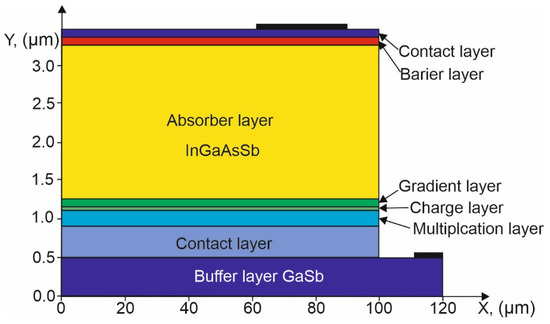
Figure 1.
Structure of the analyzed npBp barrier APD.
Table 2.
InGaAsSb-based barrier APD structure.
The theoretical simulation energy band profile of the APD is shown in Figure 2. In this structure, an electron barrier is created, allowing for the transport of minority carriers (holes) from the AL to the upper CL while blocking electron transport. However, in the analyzed case, there is also a small potential barrier in the conduction band near the p-n junction, which may block the flow of minority electrons from the AL to the p-n junction and thus reduce the photocurrent. This barrier vanishes at reverse bias U = 15 V [punch-through voltage at which the depletion region extends through the charge layer to the edge of the AL (see dashed Fermi line in Figure 2b)]. Below the punch-through voltage, the photocurrent is typically low because many of the photogenerated carriers in the AL do not have sufficient energy to cross the heterojunction interfaces.
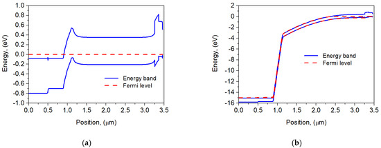
Figure 2.
Band structure of the APD barrier detector at 300 K for U = 0 V (a) and U = 15 V (b). The position of the Fermi level has been marked with a dashed line.
3. Results and Discussion
The influence of the detector layer parameters on the dark current and the photocurrent was analyzed. Numerical simulations were performed for incident radiation with power p = 0.1 − 10 W and wavelength λ = 1.55 μm. Figure 3 shows the dark and light currents under the reverse bias at T = 300 K. The punch-through voltage (reverse) was estimated at the level of 10.5 V, and the breakdown voltage was 58.4 V. When the APD reaches the punch-through voltage, the p–n-junction depletion begins to extend to the InGaAsSb AL, the charge layer barrier in the conduction band vanishes, and the photogenerated carriers move to the ML. The photocurrent for U ≤ Upt results from the optical generation of carriers in the contact and the multiplication layers.
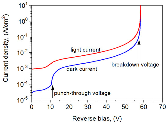
Figure 3.
Theoretical simulation of the dark current and photocurrent densities for the reverse-biased APD at T = 300 K. Incident radiation: power p = 10 W and wavelength λ = 1.55 μm.
The precise determination of the punch-through voltage requires analysis of the detector band structure and I-V characteristics. Figure 4 shows the dependence of the dark current and photocurrent on the voltage near Upt (Figure 4a) and the shape of the energy bands and the position of the quasi-Fermi levels at the reverse bias of 9 V and 15 V. The punch-through effect on the I-V characteristics appears at a reverse bias of 10.5 V. Below this voltage (for U = −9 V), a small barrier in the conduction band was observed, which disappeared at voltages above −11 V, causing a significant increase in the photocurrent. At the same time, the splitting of the quasi-Fermi levels increases, which at a voltage of −15 V reaches a value comparable to the absorber energy gap. This indicates the expansion of the depletion region to the entire AL. Also, part of the electric field drops in the absorber region, facilitating the transport of electrons to the multiplication region. When the operating voltage is between −15 V and −58.4 V, the APD operates in a linear mode. The number of carriers being multiplicated increases and the photocurrent is multiplied, with a gain of up to 200. When the APD operates between Upt and 95% of Ubr, the photocurrent increases from 3.3 × 10⁻³ A/cm2 to 9.7 × 10⁻² A/cm2, while the dark current increases from 7.8 × 10⁻⁴ A/cm2 to 2.7 × 10⁻² A/cm2.
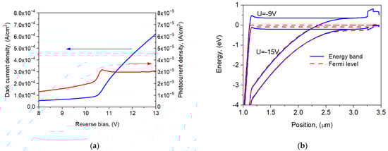
Figure 4.
Dark current and photocurrent versus voltage near Upt (a) and the AL band structure for U = −9 V and U = −15 V (b) at T = 300 K. The position of the Fermi level has been marked with a dashed line.
An analysis of the electric field distribution and impact ionization rate was performed. Figure 5 shows the comparison of the electric field distribution and impact ionization rate for the npBp APD with the parameters presented in Table 2 at a reverse bias of 0.95 × Ubr = −55.5 V.
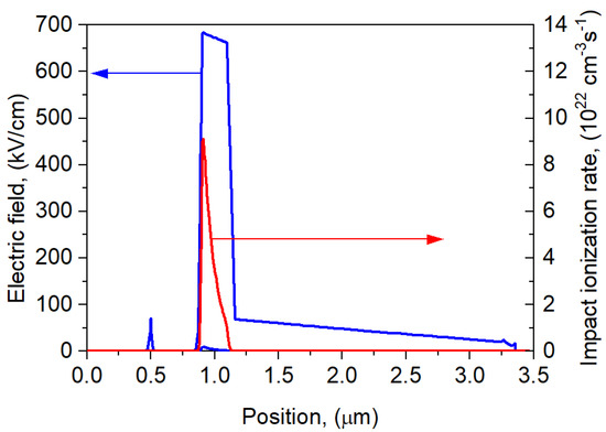
Figure 5.
Electric field and impact ionization distribution along npBp detector at U = −55.5 V at T = 300 K.
The electric field distribution is typical for APDs. A high field of the order of 700 kV/cm occurs only in the ML, while in the charge, gradient, and absorber layers, there is a 10-times-lower field causing a drift of minority carriers (electrons) towards the ML and the p-n junction. Impact ionization occurs mainly in the ML region near the p-n junction.
To assess the impact of the ionization contribution, the electric field and carrier concentration distribution at the Upt and 0.95 × Ubr reverse bias conditions were analyzed and are presented in Figure 6. The electric field (see Figure 6a) in the AL increases faster than that in the ML. The electron and hole concentrations increased versus the reverse bias (Figure 6b). On the other hand, in the depleted absorber, the photogenerated electrons and the multiplied holes from the ML significantly affect the transport characteristics.
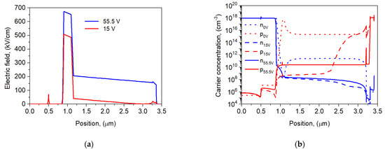
Figure 6.
Electric field distribution (a) and electron and hole concentrations at U = −15 V and U = −55.5 V (b) for the npBp APD at 300 K. The position of the equilibrium concentration has been marked with a dotted line.
The influence of the charge layer doping on the dark current and electric field distribution for the npBp APD was analyzed, and the results are presented in Figure 7. Figure 7a shows that with higher CL doping, the Ubr is lower but the Upt is higher and the linear part of the I-V characteristic is reduced. This is connected with the decrease in the electric field in the ML versus CL doping, as shown in Figure 7b. The charge layer serves as an electric field control layer, ensuring that the electric field in the ML is sufficient to reach a high gain while simultaneously reducing the field in the AL below the tunneling threshold to maintain a low dark current.
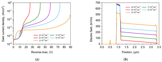
Figure 7.
I-V characteristics (a) and electric field distribution at 0.95 × Ubr (b) for npBp APD at T = 300 K with selected charge layer doping p = 2 × 10¹⁷, 5 × 10¹⁷, 6 ×10¹⁷, 7 × 10¹⁷, 8 × 1017 cm−3.
The CL doping significantly affects the photocurrent and APD’s gain. Figure 8a shows the theoretical simulation of the photocurrent density versus the reverse bias for CL selected doping at 300 K. The increase in the CL doping causes an increase in the photocurrent but decreases Ubr (Figure 8a). For voltages near Ubr (0.95 × Ubr), the gain varied from 30 to 40, with the charge layer doping varying from 8 × 1017 cm−3 to 2 × 1017 cm−3. The dependence of the electric field E on the applied voltage was determined, and then the dependence of the k coefficient on the bias was extracted. We can see that in the avalanche multiplication range, the k value changed from 0.02 to 0.08. The k and M allowed us to determine the excess noise factor F(M) according to the relation (1). F(M) is presented in Figure 8b for selected levels of charge layer doping. The excess noise factor increases versus gain and lowering the doping level of the charge layer.
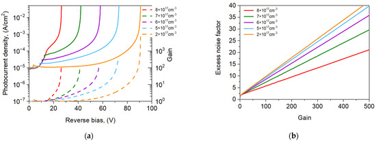
Figure 8.
Photocurrent gain (a) and excess noise factor (b) for npBp APD at 300 K with selected charge layer doping p = 2 × 10¹⁷, 5 × 10¹⁷, 6×10¹⁷, 7 × 10¹⁷, 8 × 1017 cm−3.
The influence of the ML parameters on the I-V characteristics and photocurrent gain was also analyzed. Figure 9 shows the influence of the ML doping level on the dark current and photocurrent for the tested npBn detector at 300 K. An increase in the dopant concentration in the ML by one order causes a slight increase in gain and a decrease in the avalanche breakdown voltage Ubr by several volts. This effect is caused by the electric field increase in the absorber region at the expense of the reduction in the field in the ML.
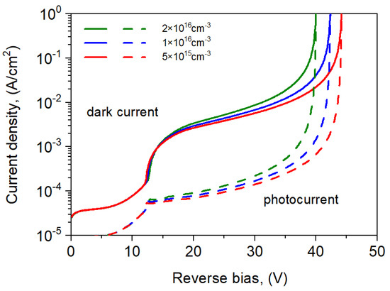
Figure 9.
Dark current and photocurrent densities for the npBp APD at T = 300 K for selected ML doping: p = 5 × 10¹⁵, 1 × 10¹⁶, 2 × 1016 cm−3.
The influence of the ML thickness on the avalanche multiplication rate is more pronounced. The simulated I-V characteristics for the selected ML thicknesses are shown in Figure 10. The punch-through voltage Upt increases versus ML width, while the breakdown voltage decreases. The photocurrent and the avalanche gain increase versus ML thickness, but at the same time the voltage range of the ML decreases.
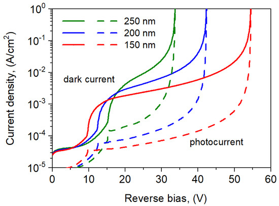
Figure 10.
Dark current and photocurrent densities for the npBp APD at T = 300 K for selected ML thickness: d = 150, 200, and 250 nm.
Figure 11 shows a comparison of the theoretically simulated I-V characteristics for the analyzed npBp barrier detectors from our work with literature data according to Ref. [15]. The presented literature data do not correspond to the analyzed structure, i.e., they differ in the stoichiometric composition of the AL and its doping level as well as in the ML material and geometrical dimensions. The In0.22Ga0.78As0.19Sb0.81 absorber had a thickness of 1.4 µm and a p-type doping level of 1 × 1016 cm−3. The ML was made from AlGaAsSb. Hence, this detector was characterized by a breakdown voltage of 15 V and a punch-through voltage of 12.5 V at a temperature of 300 K. In the work [15], IR illumination was carried out using an Eblana Photonics 2.1 μm fiber-coupled laser, but we calculated an illumination power of p = 10 W and a wavelength of λ = 1.55 μm. The gain was defined as the photocurrent ratio at a given voltage to the photocurrent at the punch-through voltage. Minor differences in illumination do not significantly affect the current gain. Figure 11 presents the npBp avalanche detector reaching a significantly (about two orders of magnitude) lower dark current and comparable gain to the detector presented in the literature.
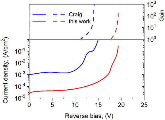
Figure 11.
Comparison of the simulated theoretical I-V characteristics and gain for the analyzed npBp APD at T = 300 K with data according to [15].
4. Conclusions
This paper presents an analysis of the avalanche parameters of npBp IR barrier detectors based on a quaternary AIIIBV InGaAsSb material, which was lattice-matched to the GaSb substrate and operated at 300 K. Despite small discontinuity in the conduction band, a significant impact of the charge layer on the detector avalanche parameters was demonstrated. The doping level of the charge layer influences the dark current and photocurrent and changes the multiplication gain and breakdown voltage. As the doping of the charge layer increases, the dark current and photocurrent increase but the excess noise factor and breakdown voltage decrease. The proposed detector structure allows for obtaining comparable gain and lower dark currents in relation to the APD detectors made of InGaAsSb previously presented in the literature. The performed simulations confirmed the possibility of developing avalanche detectors with high gain at room temperature made of quaternary InGaAsSb materials.
Author Contributions
Conceptualization, P.M., K.K., J.R. and S.K.; methodology, T.M.; software, T.M.; validation, P.M., J.R. and S.K.; formal analysis, P.M. and J.R.; investigation, P.M., N.G. and S.K.; resources, T.M.; data curation, T.M. and N.G.; writing—original draft preparation, J.R. and P.M.; writing—review and editing, P.M., N.G. and S.K.; visualization, P.M.; supervision, P.M.; project administration, P.M. and K.K.; funding acquisition, P.M., K.K. and S.K. All authors have read and agreed to the published version of the manuscript.
Funding
This research was funded by the National Centre for Research and Development grant: INNOGLOBO/II/65/PfBaAIRD/2023.
Institutional Review Board Statement
Not applicable.
Informed Consent Statement
Not applicable.
Data Availability Statement
The original contributions presented in this study are included in the article. Further inquiries can be directed to the corresponding author.
Conflicts of Interest
Author K.K. was employed by the company Photin sp. Z o.o. The remaining authors declare that the research was conducted in the absence of any commercial or financial relationships that could be construed as a potential conflict of interest.
References
- Saleh, M.A.; Hayat, M.M.; Sotirelis, P.P.; Holmes, A.L.; Campbell, J.C.; Saleh, B.E.A.; Teich, M.C. Impact-ionization and noise characteristics of thin III-V avalanche photodiodes. IEEE Trans. Electron Devices 2001, 48, 2722–2731. [Google Scholar] [CrossRef]
- Chen, J.; Zhang, Z.; Zhu, M.; Xu, J.; Li, X. Optimization of InGaAs/InAlAs Avalanche Photodiodes. Nanoscale Res. Lett. 2017, 12, 33. [Google Scholar] [CrossRef]
- Meng, X.; Tan, C.H.; Dimler, S.; David, J.P.R.; Ng, J.S. 1550 nm InGaAs/InAlAs single photon avalanche diode at room temperature. Opt. Express 2014, 22, 22608. [Google Scholar] [CrossRef] [PubMed]
- Jiang, Y.; Chen, J. Optimization of the Linearity of InGaAs/InAlAs SAGCM APDs. J. Light. Technol. 2019, 37, 3459–3464. [Google Scholar] [CrossRef]
- Martyniuk, P.; Wang, P.; Rogalski, A.; Gu, Y.; Jiang, R.; Wang, F.; Hu, W. Infrared avalanche photodiodes from bulk to 2D materials. Light. Sci. Appl. 2023, 12, 212. [Google Scholar] [CrossRef] [PubMed]
- Guo, Z.; Wang, W.; Li, Y.; Qu, H.; Fan, L.; Chen, X.; Zhu, Y.; Gu, Y.; Wang, Y.; Zheng, C.; et al. Material Defects and Dark Currents in InGaAs/InP Avalanche Photodiode Devices. IEEE Trans. Electron Devices 2022, 69, 4944–4949. [Google Scholar] [CrossRef]
- Liu, W.; Shi, Z.; Gao, J. Enhanced initial photocurrent caused by the multiplication process at punch-through voltage in InGaAs/InP avalanche photodiode with highly doped charge layer. Infrared Phys. Technol. 2022, 124, 104218. [Google Scholar] [CrossRef]
- Zhang, S.; Zhao, Y. Study on impact ionization in charge layer of InP/InGaAs SAGCM avalanche photodiodes. Opt. Quantum Electron. 2015, 47, 2689–2696. [Google Scholar] [CrossRef]
- Ma, Y.-J.; Zhang, Y.-G.; Gu, Y.; Chen, X.-Y.; Zhou, L.; Xi, S.-P.; Li, H.-S.-B.-Y. Low Operating Voltage and Small Gain Slope of InGaAs APDs with p-Type Multiplication Layer. IEEE Photonics Technol. Lett. 2015, 27, 661–664. [Google Scholar] [CrossRef]
- Marshall, A.R.J.; Craig, A.P.; Reyner, C.J.; Huffaker, D.L. GaAs and AlGaAs APDs with GaSb absorption regions in a separate absorption and multiplication structure using a hetero-lattice interface. Infrared Phys. Technol. 2015, 70, 168–170. [Google Scholar] [CrossRef]
- Nada, M.; Hoshi, T.; Yamazaki, H.; Hashimoto, T.; Matsuzaki, H. Linearity improvement of high-speed avalanche photodiodes using thin depleted absorber operating with higher order modulation format. Opt. Express 2015, 23, 27715. [Google Scholar] [CrossRef] [PubMed]
- Wang, W.; Yao, J.; Li, L.; Ge, H.; Wang, L.; Zhu, L.; Chen, Q.; Lu, H.; Chen, B. High-speed InAlAs digital alloy avalanche photodiode. Appl. Phys. Lett. 2023, 123, 191102. [Google Scholar] [CrossRef]
- Williams, G.M.; Compton, M.; Ramirez, D.A.; Hayat, M.M.; Huntington, A.S. Multi-Gain-Stage InGaAs Avalanche Photodiode With Enhanced Gain and Reduced Excess Noise. IEEE J. Electron Devices Soc. 2013, 1, 54–65. [Google Scholar] [CrossRef]
- Benker, M.; Gu, G.; Senckowski, A.; Xiang, B.; Dwyer, C.; Adams, R.; Xie, Y.; Nagarajan, R.; Li, Y.; Lu, X. Room-Temperature (RT) Extended Short-Wave Infrared (e-SWIR) Avalanche Photodiode (APD) with a 2.6 µm Cutoff Wavelength. Micromachines 2024, 15, 941. [Google Scholar] [CrossRef]
- Craig, A.P.; Jain, M.; Meriggi, L.; Cann, T.; Niblett, A.; Collins, X.; Marshall, A.R.J. Extended short-wave infrared linear and Geiger mode avalanche photodiodes, based on 6.1 Å materials. Appl. Phys. Lett. 2019, 114, 053501. [Google Scholar] [CrossRef]
- Dadey, A.A.; Jones, A.H.; March, S.D.; Bank, S.R.; Campbell, J.C. Separate absorption, charge, and multiplication staircase avalanche photodiodes. Appl. Phys. Lett. 2024, 124, 081101. [Google Scholar] [CrossRef]
- Ren, M.; Maddox, S.J.; Woodson, M.E.; Chen, Y.; Bank, S.R.; Campbell, J.C. AlInAsSb separate absorption, charge, and multiplication avalanche photodiodes. Appl. Phys. Lett. 2016, 108, 191108. [Google Scholar] [CrossRef]
- Ronningen, T.J.; Kodati, S.H.; Jin, X.; Lee, S.; Jung, H.; Tao, X.; Lewis, H.I.J.; Schwartz, M.; Gajowski, N.; Martyniuk, P.; et al. Ionization coefficients and excess noise characteristics of AlInAsSb on an InP substrate. Appl. Phys. Lett. 2023, 123, 131110. [Google Scholar] [CrossRef]
- Li, N.; Sun, J.; Jia, Q.; Song, Y.; Jiang, D.; Wang, G.; Xu, Y.; Niu, Z. High Performance nBn Detectors Based on InGaAsSb Bulk Materials for Short Wavelength Infrared Detection. AIP Adv. 2019, 9, 105106. [Google Scholar] [CrossRef]
- Collins, X.; White, B.; Cao, Y.; Osman, T.; Taylor-Mew, J.; Ng, J.S.; Tan, C.H. Low-noise AlGaAsSb avalanche photodiodes for 1550 nm light detection. In Optical Components and Materials XIX; Digonnet, M.J., Jiang, S., Eds.; SPIE: San Francisco, CA, USA, 2022; p. 16. [Google Scholar] [CrossRef]
- Sheridan, B.; Collins, X.; Taylor-Mew, J.; White, B.; Ng, J.S.; Tan, C.H. An Extremely Low Noise-Equivalent Power Photoreceiver Using High-Gain InGaAs/AlGaAsSb APDs. J. Light. Technol. 2025, 43, 741–746. [Google Scholar] [CrossRef]
- Jin, X.; Zhao, S.; Craig, A.P.; Tian, O.; Gilder, L.; Yi, X.; Carmichael, M.; Golding, T.; Tan, C.H.; Marshall, A.R.J.; et al. High-performance room temperature 2.75 µm cutoff In0.22Ga0.78As0.19Sb0.81/Al0.9Ga0.1As0.08Sb0.92 avalanche photodiode. Optica 2024, 11, 1632–1638. [Google Scholar] [CrossRef]
- Crosslight Device Simulation Software-General Manual; Crosslight Software Inc.: Vancouver, BC, Canada, 2019.
- Ji, X.; Liu, B.; Xu, Y.; Tang, H.; Li, X.; Gong, H.; Shen, B.; Yang, X.; Han, P.; Yan, F. Deep-Level Traps Induced Dark Currents in Extended Wavelength InxGa1−xAs/InP Photodetector. J. Appl. Phys. 2013, 114, 224502. [Google Scholar] [CrossRef]
- Moussa, R.; Abdiche, A.; Abbar, B.; Guemou, M.; Riane, R.; Murtaza, G.; Omran, S.B.; Khenata, R.; Soyalp, F. Ab Initio Investigation of the Structural, Electronic and Optical Properties of Cubic GaAs1−xPx Ternary Alloys Under Hydrostatic Pressure. J. Electron. Mater. 2015, 44, 4684–4699. [Google Scholar] [CrossRef]
- Kim, J.O.; Nguyen, T.D.; Ku, Z.; Urbas, A.; Kang, S.-W.; Lee, S.J. Short Wavelength Infrared Photodetector and Light Emitting Diode Based on InGaAsSb. In Infrared Technology and Applications XLIII; Andresen, B.F., Fulop, G.F., Hanson, C.M., Miller, J.L., Norton, P.R., Eds.; Proceedings of SPIE: San Francisco, CA, USA, 2017; Volume 10177, p. 101772M. [Google Scholar] [CrossRef]
- Schaefer, S.T.; Gao, S.; Webster, P.T.; Kosireddy, R.R.; Johnson, S.R. Absorption Edge Characteristics of GaAs, GaSb, InAs, and InSb. J. Appl. Phys. 2020, 127, 165705. [Google Scholar] [CrossRef]
- Craig, A.P.; Jain, M.; Wicks, G.; Golding, T.; Hossain, K.; McEwan, K.; Howle, C.; Percy, B.; Marshall, A.R.J. Short-Wave Infrared Barriode Detectors Using InGaAsSb Absorption Material Lattice Matched to GaSb. Appl. Phys. Lett. 2015, 106, 201103. [Google Scholar] [CrossRef]
- Shim, K.; Rabitz, H.; Dutta, P. Band Gap and Lattice Constant of GaxIn1−xAsySb1−y. J. Appl. Phys. 2000, 88, 7157–7161. [Google Scholar] [CrossRef]
- Vurgaftman, I.; Meyer, J.R.; Ram-Mohan, L.R. Band Parameters for III–V Compound Semiconductors and Their Alloys. J. Appl. Phys. 2001, 89, 5815–5875. [Google Scholar] [CrossRef]
- Manyk, T.; Rutkowski, J.; Kopytko, M.; Kłos, K.; Martyniuk, P. Theoretical Study of Quaternary nBp InGaAsSb SWIR Detectors for Room Temperature Condition. Materials 2024, 17, 5482. [Google Scholar] [CrossRef]
- Chynoweth, A.G. Ionization Rates for Electrons and Holes in Silicon. Phys. Rev. 1958, 109, 1537–1540. [Google Scholar] [CrossRef]
Disclaimer/Publisher’s Note: The statements, opinions and data contained in all publications are solely those of the individual author(s) and contributor(s) and not of MDPI and/or the editor(s). MDPI and/or the editor(s) disclaim responsibility for any injury to people or property resulting from any ideas, methods, instructions or products referred to in the content. |
© 2025 by the authors. Licensee MDPI, Basel, Switzerland. This article is an open access article distributed under the terms and conditions of the Creative Commons Attribution (CC BY) license (https://creativecommons.org/licenses/by/4.0/).