Article

High-Performance Hydrogen Gas Sensor Based on Pd-Doped MoS2/Si Heterojunction

School of Materials Science and Engineering, China University of Petroleum, Qingdao 266580, China
*
Author to whom correspondence should be addressed.
Sensors 2025, 25(15), 4753; https://doi.org/10.3390/s25154753 (registering DOI)
Submission received: 7 July 2025 / Revised: 30 July 2025 / Accepted: 30 July 2025 / Published: 1 August 2025
(This article belongs to the Special Issue 2D Materials for Advanced Sensing Technology)

Abstract

High-performance hydrogen gas sensors have gained considerable interest for their crucial function in reducing H2 explosion risk. Although MoS2 has good potential for chemical sensing, its application in hydrogen detection at room temperature is limited by slow response and incomplete recovery. In this work, Pd-doped MoS2 thin films are deposited on a Si substrate, forming Pd-doped MoS2/Si heterojunctions via magnetron co-sputtering. The incorporation of Pd nanoparticles significantly enhances the catalytic activity for hydrogen adsorption and facilitates more efficient electron transfer. Owing to its distinct structural characteristics and sharp interface properties, the fabricated Pd-doped MoS2/Si heterojunction device exhibits excellent H2 sensing performance under room temperature conditions. The gas sensor device achieves an impressive sensing response of ~6.4 × 10³% under 10,000 ppm H2 concentration, representing a 110% improvement compared to pristine MoS2. Furthermore, the fabricated heterojunction device demonstrates rapid response and recovery times (24.6/12.2 s), excellent repeatability, strong humidity resistance, and a ppb-level detection limit. These results demonstrate the promising application prospects of Pd-doped MoS2/Si heterojunctions in the development of advanced gas sensing devices.

1. Introduction

Hydrogen gas (H2) holds significant potential in renewable energy transitions because it is clean, eco-friendly, renewable, and abundant. It has the capacity to improve air quality, mitigate global warming, and serve as a sustainable substitute for fossil fuels in both industry and transportation [1,2,3]. However, due to its high flammability in air within a concentration range of 4% to 75.6% [4], the real-time and precise detection of H2 levels is essential for practical applications. In the past few decades, numerous resistive hydrogen sensors based on metal oxide semiconductor materials have been studied, including In2O3, Pd/V2O5, and SnO2 nanofibers [5,6,7]. However, these oxides usually require high operating temperatures above 300 °C. This not only results in higher power consumption, but also raises safety concerns due to hydrogen becoming highly flammable at elevated temperatures [8,9,10,11,12,13]. To address this challenge, it is crucial to develop H2 sensors capable of detecting trace amounts of hydrogen with rapid response at room temperature.
Two-dimensional (2D) materials, such as graphene, phosphorene, and transition metal dichalcogenides (TMDs), have garnered considerable attention as promising candidates for next-generation electronic devices, thanks to their exceptional electrical and mechanical characteristics and their large specific surface areas [14,15,16,17]. Among TMDs, MoS2 is particularly notable for its layered structure, where strong covalent bonds connect atoms within individual layers, while adjacent layers are held together by comparatively weak van der Waals forces. This structural arrangement increases the specific surface area, facilitating better contact with gas molecules. Furthermore, MoS2 exhibits an adjustable band gap between 1.2 and 1.9 eV, which can be tuned by varying the thickness of its layers [18]. Various studies have explored the use of few-layered MoS2 for gas sensing, demonstrating its capability to detect NH3, NO, H2O, and many other chemical vapors [19,20,21,22,23,24]. However, its basal planes are electrochemically inert and poorly conductive, which limits its ability to detect nonpolar gases like H2 [25]. Fortunately, structural imperfections—such as defects, vacancies, and dangling bonds—especially at edge sites or introduced during fabrication, can serve as active centers for gas adsorption and charge transfer [26].
To overcome the limitations of inert basal planes, recent research has explored the integration of noble metal catalysts to enhance surface reactivity and gas-sensing performance [27,28,29]. Among them, Pd stands out as an efficient catalyst for H2 detection. For example, Jaiswal et al. fabricated Pd-decorated MoS2 hybrid films, achieving enhanced hydrogen response due to nanoscale structural modulation [28]. Similarly, Baek et al. deposited Pd onto MoS2 films prepared by solution methods. The Pd catalyst facilitated H2 dissociation and spillover onto the sensing layer, resulting in superior sensing behavior [29]. Despite these promising results, achieving uniform distribution and controlled loading of noble metals in MoS2-based sensors remains a challenge. Effective H2 dissociation relies heavily on optimizing both the surface coverage and Pd content. To address this, magnetron co-sputtering has been adopted, enabling precise control of Pd nanoparticles doping while ensuring high coverage, uniformity, and crystallinity of the MoS2 films [30,31]. Due to interfacial effects, the heterojunction formed by sputtering MoS2 onto a silicon substrate is expected to enhance its gas sensing performance further. Wu et al. reported the construction of MoS2/Si nanowire array heterojunctions that achieved ultrahigh sensitivity for NO detection at room temperature, attributed to charge trapping and interfacial modulation effects [32]. Moreover, MoS2/Si heterojunctions were used as hydrogen sensors, but exhibited extremely long response times of approximately 443.5 s, which severely limits their practical application [33]. This highlights the need for optimizing the interfacial structure to improve performance. However, to the best of our knowledge, there are currently no reports on hydrogen sensors based on Pd-doped MoS2/Si heterojunctions. This indicates a research gap in simultaneously utilizing Pd nanoparticle doping and heterostructure engineering under room temperature conditions.
The aim of this study is to develop a high-performance hydrogen gas sensor operating at room temperature, based on Pd-doped MoS2/Si heterojunctions prepared via magnetron co-sputtering. By precisely controlling both the doping of Pd nanoparticles and the formation of the heterojunction interface, the sensor can synergistically improve hydrogen adsorption, electron transfer, and dynamic sensing behavior. The fabricated Pd-doped MoS2/Si heterojunction exhibited an excellent H2 sensing response (6.4 × 10³%), faster response/recovery times (24.6/12.2 s), outstanding repeatability, strong resistance to humidity, and a ppb-level detection limit. This study delivers a promising strategy to the design and optimization of high-response hydrogen sensors, offering strong potential for next-generation gas sensor applications.

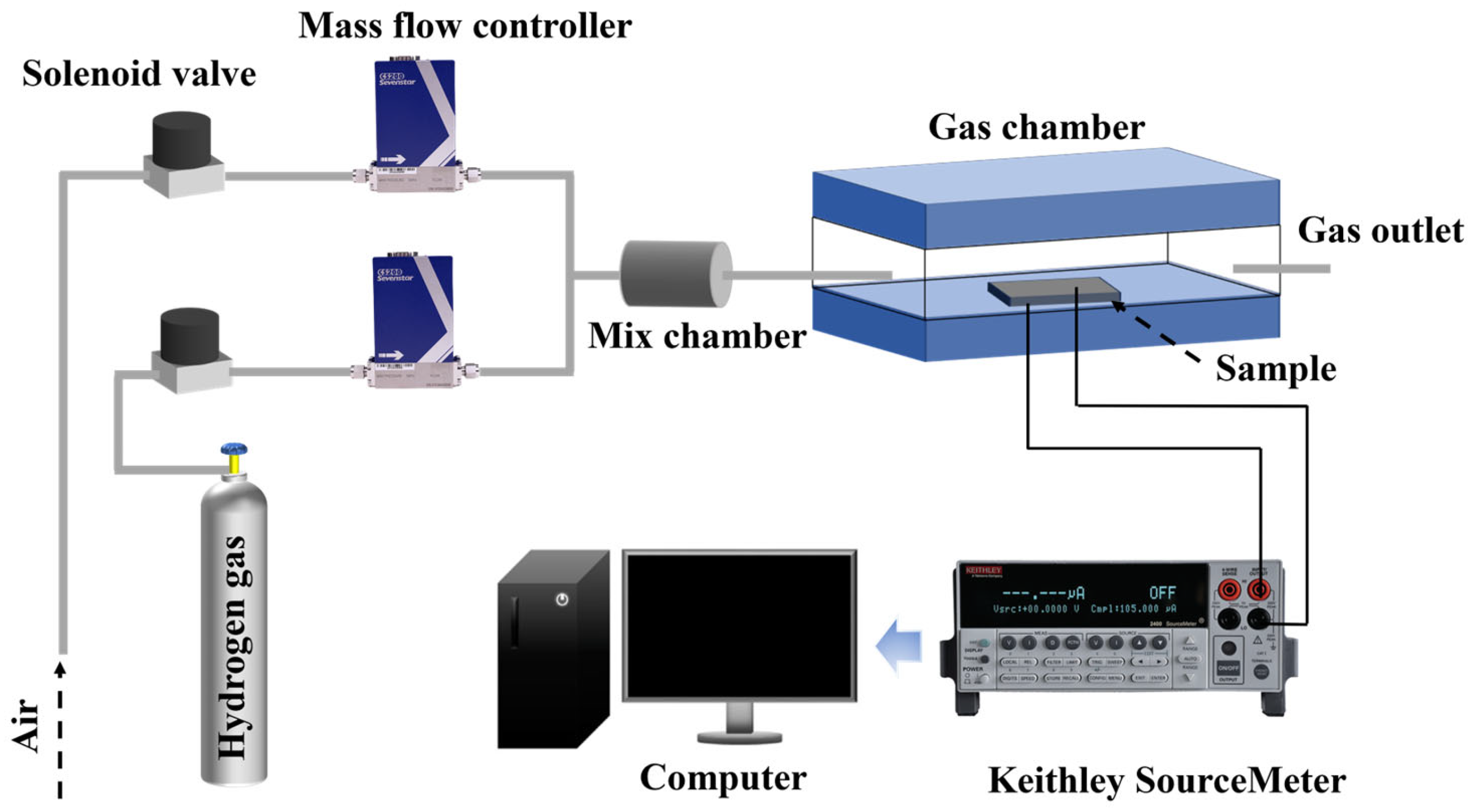
2. Materials and Methods

n-type silicon wafers with a (100) crystallographic orientation and a thickness of approximately 0.5 mm were employed. These single-crystal substrates, purchased from Suzhou Yancai Weina Technology Co., Ltd. (Nanfeng, China), had a resistivity of 1 × 10⁵ Ω·cm and a purity of 99.99%. The wafer, sliced into pieces measuring 10.0 mm × 10.0 mm, underwent sequential ultrasonic cleaning using ethanol, acetone, and deionized water. Pd-doped MoS2 thin films were grown on a Si substrate using the DC magnetron co-sputtering technique. MoS2 targets (purity 99.99%) were obtained from Zhongnuo Xincai Technology Co., Ltd. (Beijing, China), and Pd sources (purity 99.99%) were supplied by Beijing Global JinXin International Co., Ltd. (Beijing, China). During the co-sputtering process, high-purity Ar was employed as the sputtering gas under a chamber pressure of 1 Pa. The sputtering powers for Pd and MoS2 targets were set to 1.0 W and 10.0 W, respectively, and the deposition was carried out at a substrate temperature of 400 °C. Finally, Pd was deposited onto the doped MoS2 layer as the top electrode by magnetron sputtering using Ar gas at a pressure of 1 Pa and a sputtering power of 10 W, while indium (In) was manually applied to the rear side of the Si substrate using a soldering iron as the bottom electrode. Electrical measurements were performed by connecting the electrodes using 0.1 mm diameter copper wires.
The film’s surface was analyzed using a scanning electron microscope (TESCAN MIRA LMS, Brno, Czech Republic). The crystalline structure of the thin films was examined using Bruker D8 X-ray diffraction (XRD). Raman spectroscopy (HORIBA, HR800, Kyoto, Japan), employing a 532 nm excitation wavelength, was utilized to investigate the Pd-doped MoS2 thin films. X-ray photoemission spectroscopy (Thermo K-Alpha spectrometer) was performed to determine the chemical composition. The optical bandgap was assessed with a Hitachi UH4150 spectrophotometer. Figure 1 illustrates the setup employed to investigate the gas sensing characteristics of the Pd-doped MoS2/Si heterojunction. The sensor device was positioned inside a sealed chamber, integrated with a gas flow system that included gas cylinders and mass flow controllers for gas sensing experiments. These mass flow controllers, connected to the chamber’s upper ports, precisely regulated the gas flow rates, enabling the creation of H2 at varying concentrations. The I–V characteristics of the sensor, under different gas conditions, were recorded using a Keithley 2400 digital source meter.

3. Results

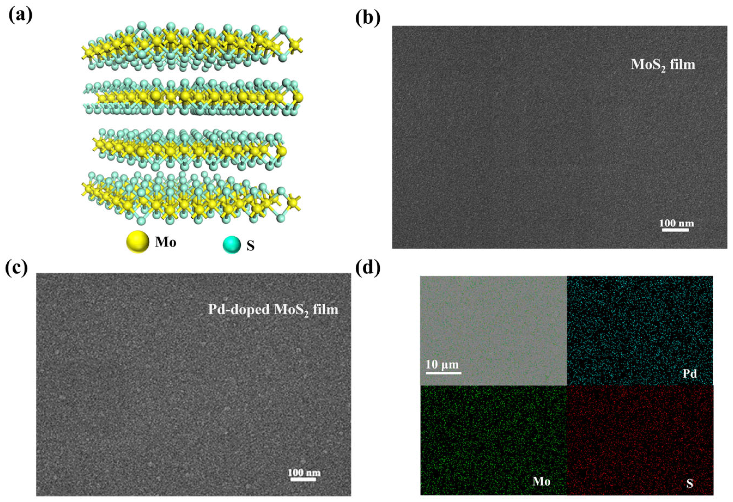
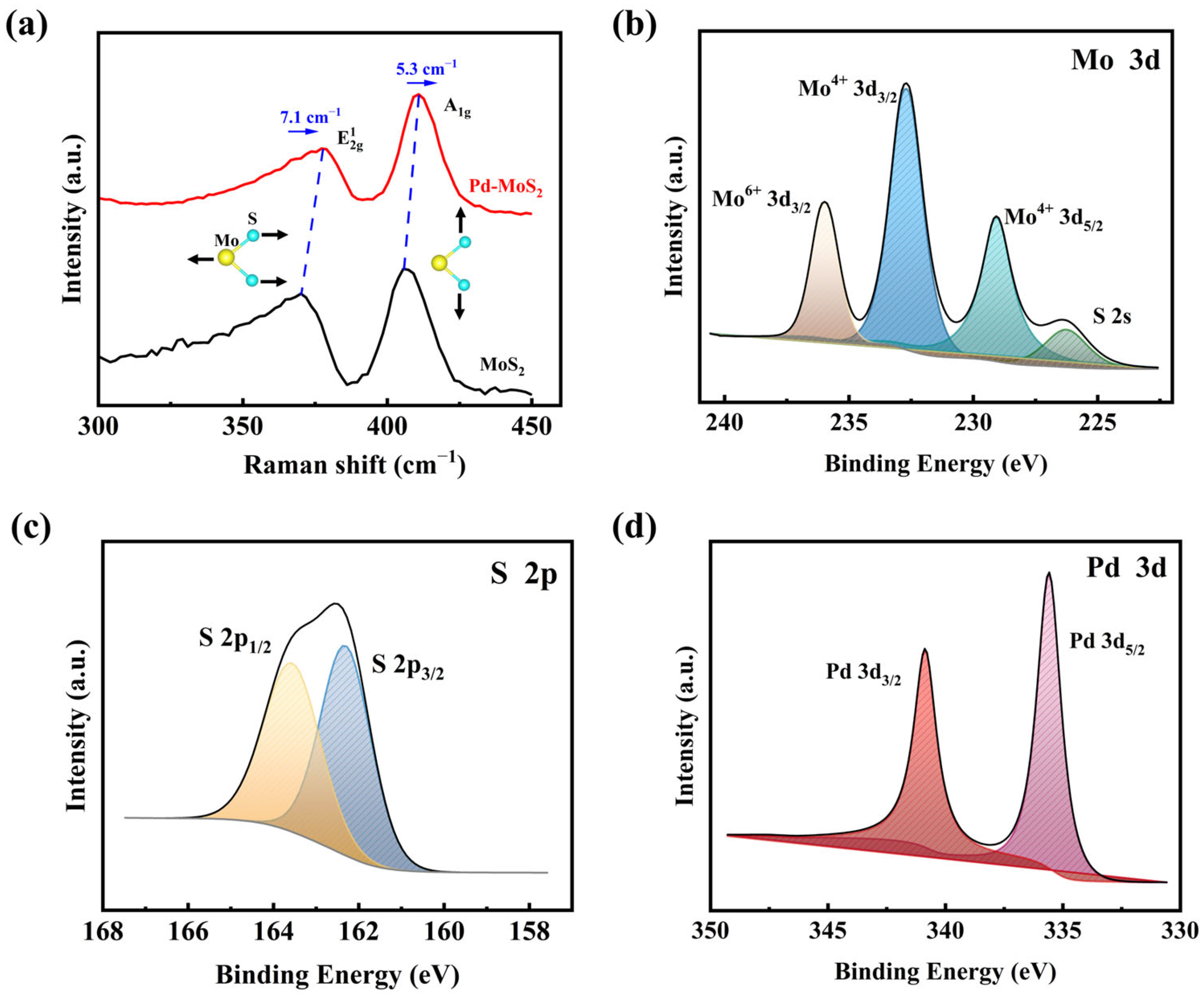
3.1. Thin Film’s Characterization

As shown in Figure 2a, bulk MoS2 possesses a layered crystalline architecture. This distinctive arrangement, coupled with the lack of dangling bonds between neighboring layers, enables the production of ultrathin MoS2 sheets characterized by smooth surfaces and large specific surface areas. To further investigate the crystal structure of the Pd-doped MoS2 thin film, XRD analysis was performed (Figure S1, Supplementary Materials). The Pd-doped MoS2 film exhibits distinct diffraction peaks at 14.4° and 51.3°, which correspond to the (003) and (018) crystal planes, respectively (PDF No. 74-0932), indicating good crystallinity and successful formation of the layered MoS2 structure. In addition, no new diffraction peaks were observed after Pd doping, suggesting that the doping concentration is relatively low and does not lead to the formation of any detectable secondary phases. Figure 2b,c show the SEM images of MoS2 films before and after Pd doping. Figure 2b displays the surface Structure of the pristine MoS2 film, revealing a smooth texture with no obvious grain boundaries. This observation suggests that the MoS2 thin film is uniformly deposited across the substrate. After Pd doping (Figure 2c), the surface becomes noticeably rougher, and clear grain boundaries appear. The increased surface roughness facilitates the introduction of more structural defects, thereby generating additional active sites for reaction with H2 molecules. Pd nanoparticles mainly occupy and interact with defect sites introduced into the MoS2 basal planes during sputtering, rather than acting on ideal, defect-free basal surfaces [34]. The microstructure and chemical composition of the Pd-doped MoS2 thin films were investigated using energy-dispersive spectroscopy (EDS). Figure 2d shows the elemental distribution map obtained from the film’s planar view. The Pd element is very uniformly distributed within the thin film, indicating that Pd nanoparticles have been successfully and homogeneously doped into the MoS2 thin film. Figure S2 (Supplementary Materials) presents the cross-sectional SEM image of the Pd-doped MoS2 film deposited on a Si substrate with a sputtering time of 1200 s. The layered structure of MoS2 is not clearly visible in the image. Instead, the film exhibits a distinctly crumpled morphology, which is markedly different from the typical flat MoS2 nanosheets and is likely attributed to the incorporation of Pd nanoparticles. The extended sputtering time was chosen to achieve better imaging contrast in SEM, and the measured film thickness is approximately 330.84 nm. However, the Pd-doped MoS2 film used in the actual gas sensing tests in this study was fabricated with a sputtering time of only 10 s. Considering a deposition rate of approximately 0.28 nm/s, and based on previous studies reporting each MoS2 layer to be about 0.7 nm thick [35], the film used in the tests is estimated to consist of about four layers, with a total thickness of approximately 2.8 nm.
Figure 3a presents the Raman spectra for both MoS2 and Pd-doped MoS2 films, revealing two characteristic peaks that correspond to the E 2 g 1 and A1g vibrational modes of MoS2 [36,37]. E 2 g 1 represents the in-plane vibrational mode parallel to the substrate, while A1g corresponds to the out-of-plane mode. In Pd-doped MoS2, both peaks exhibit a blueshift, with E 2 g 1 and A1g shifting by 7.1 cm−1 and 5.3 cm−1, respectively, compared to pristine MoS2. This blueshift indicates that Pd doping introduces p-type characteristics. The elemental composition of Pd-doped MoS2 thin films was further characterized using XPS. The Mo 3d XPS spectrum is depicted in Figure 3b. The double peaks observed at 232.88 eV (Mo 3d3/2) and 229.08 eV (Mo 3d5/2) are indicative of the Mo4+ state, respectively. The additional peaks identified at 235.74 eV and 226.58 eV correspond to Mo6+ states (due to the oxidation of surface-adsorbed oxygen) and the S 2s. Figure 3c displays peaks located at 162.31 eV and 163.56 eV corresponding to the S 2p3/2 and S 2p1/2 orbitals. This result is consistent with the reported MoS2 crystal data [38]. Pd 3d XPS spectra (Figure 3d) show characteristic double peaks at 335.48 eV and 340.78 eV, corresponding to Pd 3d5/2 and Pd 3d3/2 states of metallic Pd nanoparticles [39]. The binding energies are consistent with metallic Pd, indicating that Pd is present in the form of nanoparticles. This confirms the successful doping of Pd nanoparticles into the MoS2 matrix, with a Pd concentration of 11.6 at% in the doped sample.

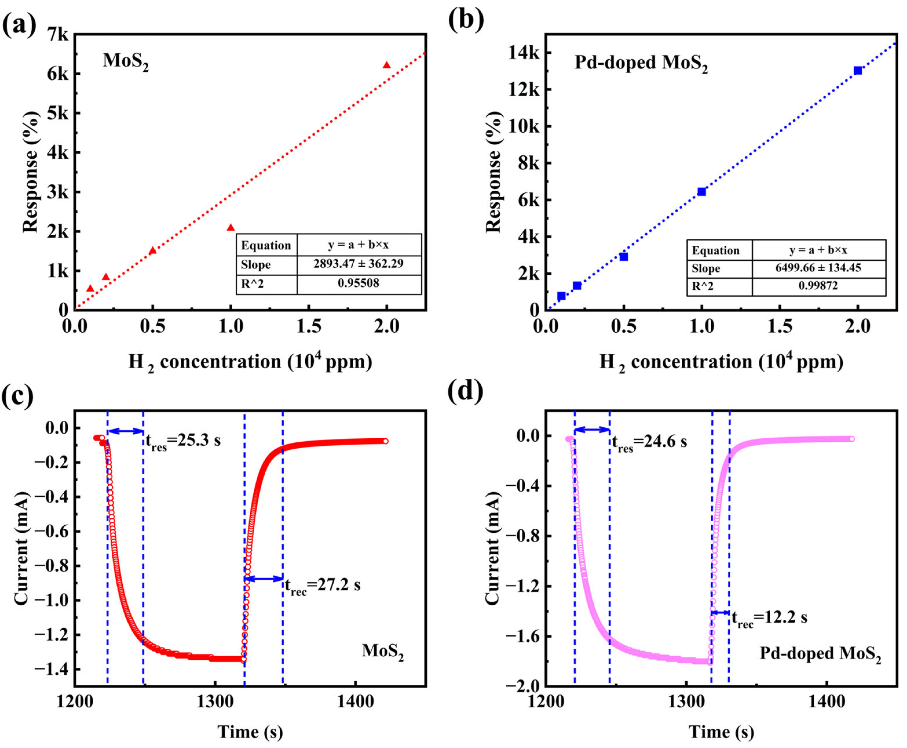
3.2. Gas Sensing Analysis

Figure 4a displays the characteristic I–V curve for the heterojunction, with an inset illustrating the measurement setup schematic. The curve exhibits pronounced rectifying behavior, achieving a rectification ratio of approximately 102 at ±1.0 V, suggesting a junction forms at the Pd-doped MoS2/Si interface. Figure 4b shows semi-logarithmic I–V plots for Pd-doped MoS2/Si heterostructure devices, measured in air and H2 environments at room temperature. As illustrated in Figure 4b, a noticeable rise in the I–V curve in the negative voltage range occurs when the sensor device is exposed to H2 instead of air, indicating that the heterojunction exhibits a distinct response to H2 exposure. The sensor response was determined according to the following equation:
s e n s o r   r e s p o n s e =   I H 2 I A i r   × 100 % .
where IH2 and IAir represent the currents measured in hydrogen and air environments, respectively. A series of MoS2 films with varying thicknesses was fabricated, and their response to 20,000 ppm hydrogen concentration was evaluated (Figure 4c). The highest sensor response was observed for a MoS2 layer thickness of approximately ~2.8 nm. Previous research has indicated that the response of MoS2 thin films decreases significantly with increasing thickness (2–16 nm) [40], which is primarily attributed to the reduced surface-to-volume ratio, ultimately leading to lower response. All subsequent experiments and discussions are based on a 2.8 nm thickness. Figure S3 (Supplementary Materials) displays the I–V characteristics of the Pd-doped MoS2/Si heterojunction exposed to 20,000 ppm H2 under varying humidity levels of 50%, 60%, 70%, and 80% RH. As the humidity rises from 50% to 80%, the current measured at 1.0 V shows a slight decline, reflecting a 51% change in response. This reduction may be attributed to the adsorption of H2O molecules on the heterojunction surface, which potentially hinders the effective interaction between hydrogen molecules and Pd nanoparticles by limiting their contact area. As shown in Figure 4d, the dynamic response of the Pd-doped MoS2/Si was measured at the hydrogen concentrations spanning from 1000 ppm to 20,000 ppm. The current response exhibits a progressive increase in amplitude as the hydrogen concentration rises. Notably, the sensor exhibits a significant response performance even at the low concentration of 1000 ppm. The limit of detection (LOD) is determined using the following equation [41]:
L O D = 3 σ n o i s e s
where σ n o i s e is the root mean square of noise and s is the slope of the response versus concentration plot. The LOD of the sensor is 360 ppb, demonstrating its great potential for applications in hydrogen detection. The repeatability of the Pd-doped MoS2/Si sensor was investigated under 10,000 ppm H2 at room temperature. According to Figure S4 (Supplementary Materials), the sensor exhibited a consistent dynamic response over 14 consecutive cycles. When alternately exposed to air and hydrogen, the device demonstrated a clear and consistent switching behavior, characterized by elevated current levels in air and suppressed currents in hydrogen. No significant variation in response was observed, indicating excellent repeatability during the switching process.
For comparison, we also evaluated the response of the undoped MoS2/Si sensor under different H2 concentrations. Figure 5a,b present the linear fitting curves of the response as a function of H2 concentration for both MoS2/Si and Pd-doped MoS2/Si devices. When the H2 concentration increases from 1000 ppm to 20,000 ppm, the response of the MoS2/Si device increases from 500% to 6200%, whereas the response of the Pd-MoS2/Si device increases from 800% to 13,000%. The sensor response exhibits a linear increase with increasing H2 concentration, and this linear fitting enables estimation of the sensor response at any H2 concentration within the range of 1000 ppm to 15,000 ppm. The calibration equations and corresponding correlation coefficients (R2) describing the relationship between H2 concentration and sensor response for both MoS2/Si and Pd-doped MoS2/Si devices are provided in Figure 5a,b. The linear fitting slope of the Pd-MoS2/Si device is significantly greater than that of the MoS2/Si device, indicating a notably enhanced response of the Pd-doped MoS2/Si sensor at each concentration level. Figure 5c shows the dynamic response and recovery behavior of the undoped MoS2/Si sensor toward 10,000 ppm H2 at room temperature, while Figure 5d presents the corresponding response curve of the Pd-doped MoS2/Si sensor under the same conditions. The response time and recovery time are defined as the specific intervals during which the sensor reaches 90% of its stable current level and returns to within 10% of its initial baseline value, respectively. The results at a hydrogen concentration of 10,000 ppm indicate that the Pd-doped MoS2/Si sensor exhibits significantly enhanced H2 sensing performance compared to the undoped MoS2 sensor. Specifically, the undoped MoS2 sensor shows a response of 2100% with a relatively slow response/recovery time of 25.3 s/27.2 s, whereas the Pd-doped MoS2/Si sensor achieves a much higher response of 6400% with faster response/recovery times of 24.6 s/12.2 s. This improvement is attributed to the higher density of active sites resulting from Pd doping, which promotes greater hydrogen adsorption, as well as the enhanced electrical conductivity, which facilitates more efficient electron transfer. As a result, both the response magnitude and response/recovery speed are considerably improved.
Based on the ultraviolet-visible absorption spectrum (UV) shown in Figure 6a, the structure becomes denser after Pd doping, allowing for greater light absorption. As a result, its absorbance is significantly improved compared to that of pure MoS2 (Figure S5, Supplementary Materials). The bandgap of the Pd-doped MoS2 thin film is approximately 1.45 eV, which is narrower than that of pure MoS2. This narrower bandgap makes it easier for electrons to be excited to the conduction band, thereby enhancing the response, which is consistent with previous studies [42]. Figure 6b illustrates the schematic diagram of electron generation and transport in the Pd-doped MoS2/Si device. When the Pd-doped MoS2 thin film is exposed to a H2 environment, the Pd nanoparticles distributed on or near the surface of MoS2 act as active catalytic sites and react with hydrogen molecules to form PdHx [43]. During this process, a large number of electrons are released from the PdHx and injected into the MoS2 thin film, thereby compensating the originally existing hole carriers and leading to a reduction in hole concentration. As the hole concentration decreases, the Fermi level of the MoS2 thin film shifts upward, moving closer to the conduction band. Figure 6c illustrates the interfacial electronic band structure formed between MoS2 and Si. According to the literature [44], the band parameters of n-type Si are as follows: work function W = 5.0 eV, conduction band minimum EC = 4.05 eV, valence band maximum EV = 5.17 eV, and bandgap Eg = 1.12 eV. Owing to the relatively elevated Fermi level of the n-type Si substrate at the interface, electrons migrate from the Si to the Pd-doped MoS2 layer. This migration persists until equilibrium is established between the Fermi levels of both materials, ultimately forming the Pd-MoS2/Si heterojunction in Figure 6d. Electrons released by the H2 reaction are injected into the Pd-MoS2 film under reverse bias and further transferred to the Pd-doped MoS2/Si interface. The accumulation of electrons at the interface causes an upward shift in the EF of Pd-MoS2, bringing it closer to EC. The reduction in interfacial energy barrier height significantly enhances the reverse current of the heterojunction [45]. Consequently, the Pd-doped MoS2/Si heterojunction exhibits unique advantages in the development of high-performance H2 sensors with superior gas response.
Table 1 compares the performance of the H2 sensors fabricated in this work with other related devices. The novelty of this work lies in the successful uniform doping of Pd nanoparticles into the MoS2 thin film using magnetron co-sputtering technology. In comparison, Pd-doped MoS2/Si heterojunctions exhibit excellent H2 sensing performance at room temperature, particularly demonstrating a higher H2 response along with significantly shorter response and recovery times. The enhanced sensing performance of the Pd-doped MoS2/Si heterojunction mainly stems from several key contributing factors: (i) The layered structure of MoS2 possesses a large specific surface area, which not only increases the contact area with gas molecules but also facilitates the regulation of structural defects and surface active sites, thereby enhancing gas adsorption and reaction performance. (ii) Appropriately doped Pd nanoparticles expose more surface active sites for hydrogen molecule adsorption and provide additional electron transport pathways, significantly improving the adsorption rate of hydrogen and the efficiency of electron transfer. (iii) Due to the sharp interface formed between Pd-doped MoS2 and Si, a significant energy barrier is established at the heterojunction, which effectively suppresses the background current under equilibrium conditions. When electrons are injected into the Pd-MoS2 layer during H2 exposure, the accumulation of charge leads to a reduction in the interfacial barrier height, thereby significantly increasing the reverse current. This dynamic modulation of the barrier enhances the device’s sensitivity to hydrogen, resulting in a more pronounced relative change in electrical response. However, to meet the demands of practical applications for faster response and shorter recovery times, there remains room for improvement in the dynamic performance of the sensor. Based on this, two effective optimization strategies are proposed in this work: (1) Structuring MoS2 into vertically aligned or edge-enriched nanoflake morphologies can substantially increase the number of exposed active edge sites and reduce gas diffusion pathways, thereby accelerating the adsorption and desorption kinetics of hydrogen molecules. Vertically aligned MoS2 films have been reported to exhibit significantly enhanced sensitivity and faster switching behavior compared to their basal-plane counterparts in gas sensing applications [46]. (2) Applying mild O2 plasma treatment can effectively passivate deep-level trap states by filling sulfur vacancies with oxygen-containing species, which leads to improved carrier mobility and a substantial reduction in response and recovery times. These strategies are expected to significantly enhance the sensing speed and real-time performance of the Pd-doped MoS2/Si device.

4. Conclusions

In summary, the Pd-doped MoS2/Si heterojunction was successfully developed, exhibiting excellent H2 detection performance. The deposited MoS2 films possess high crystallinity with uniformly distributed nanoparticles, while Pd doping exposes more active sites for H2 molecule adsorption and enhances the efficiency of electron transfer. As a result, the Pd-doped MoS2/Si heterojunction device achieves a high response of 6.4 × 10³%, fast response and recovery times of 24.6/12.2 s, excellent repeatability, strong humidity resistance, and a ppb-level detection limit at room temperature. These findings demonstrate the potential of Pd-doped MoS2/Si heterojunctions for high-performance H2 sensor applications.

Supplementary Materials

The following supporting information can be downloaded at: https://www.mdpi.com/article/10.3390/s25154753/s1. Figure S1: X-ray diffraction (XRD) θ–2θ pattern of the Pd-doped MoS2 films; Figure S2: Cross-sectional SEM micrographs of Pd-doped MoS2 layers grown on silicon wafers with a sputtering time of 1200 s; Figure S3: I–V characteristics of the Pd-doped MoS2/Si heterojunction exposed to 20,000 ppm H2 under varying humidity levels of 50%, 60%, 70%, and 80% RH; Figure S4: Repeatability of the fabricated Pd-doped MoS2/Si sensor at room temperature when exposed to 10,000 ppm H2; Figure S5: The UV absorption spectrum of MoS2 films.

Author Contributions

Conceptualization, E.M. and Z.X.; methodology, A.S.; validation, S.Y.; formal analysis, J.J.; investigation, E.M.; resources, Z.X.; writing—original draft preparation, E.M.; writing—review and editing, J.J.; visualization, E.M. All authors have read and agreed to the published version of the manuscript.

Funding

This research received no external funding.

Institutional Review Board Statement

Not applicable.

Informed Consent Statement

Not applicable.

Data Availability Statement

The authors confirm that the data supporting the findings of this study are available within the article.

Conflicts of Interest

The authors declare no conflicts of interest.

References

  1. Megía, P.J.; Vizcaíno, A.J.; Calles, J.A.; Carrero, A. Hydrogen production technologies: From fossil fuels toward renewable sources. A mini review. Energy Fuels 2021, 35, 16403–16415. [Google Scholar] [CrossRef]
  2. Kulagin, V.A.; Grushevenko, D.A. Will hydrogen be able to become the fuel of the future? Therm. Eng. 2020, 67, 189–201. [Google Scholar] [CrossRef]
  3. Calabrese, M.; Portarapillo, M.; Di Nardo, A.; Venezia, V.; Turco, M.; Luciani, G.; Di Benedetto, A. Hydrogen Safety Challenges: A Comprehensive Review on Production, Storage, Transport, Utilization, and CFD-Based Consequence and Risk Assessment. Energies 2024, 17, 1350. [Google Scholar] [CrossRef]
  4. Yang, F.; Wang, T.; Deng, X.; Dang, J.; Huang, Z.; Hu, S.; Li, Y.; Ouyang, M. Review on hydrogen safety issues: Incident statistics, hydrogen diffusion, and detonation process. Int. J. Hydrogen Energy 2021, 46, 31467–31488. [Google Scholar] [CrossRef]
  5. Sanger, A.; Kumar, A.; Kumar, A.; Jaiswal, J.; Chandra, R. A Fast Response/Recovery of Hydrophobic Pd/V2O5 Thin Films for Hydrogen Gas Sensing. Sens. Actuators B Chem. 2016, 236, 16–26. [Google Scholar] [CrossRef]
  6. Ab Kadir, R.; Li, Z.; Sadek, A.Z.; Abdul Rani, R.; Zoolfakar, A.S.; Field, M.R.; Ou, J.Z.; Chrimes, A.F.; Kalantar-zadeh, K. Electrospun Granular Hollow SnO2 Nanofibers Hydrogen Gas Sensors Operating at Low Temperatures. J. Phys. Chem. C 2014, 118, 3129–3139. [Google Scholar] [CrossRef]
  7. Mondal, B.; Gogoi, P.K. Nanoscale Heterostructured Materials Based on Metal Oxides for a Chemiresistive Gas Sensor. ACS Appl. Electron. Mater. 2022, 4, 59–86. [Google Scholar] [CrossRef]
  8. Tien, L.C.; Sadik, P.W.; Norton, D.P.; Voss, L.F.; Pearton, S.J.; Wang, H.T.; Kang, B.S.; Ren, F.; Jun, J.; Lin, J. Hydrogen Sensing at Room Temperature with Pt-Coated ZnO Thin Films and Nanorods. Appl. Phys. Lett. 2005, 87, 222106. [Google Scholar] [CrossRef]
  9. Wang, Y.; Liu, B.; Cai, D.; Li, H.; Liu, Y.; Wang, D.; Wang, L.; Li, Q.; Wang, T. Room-Temperature Hydrogen Sensor Based on Grain-Boundary Controlled Pt Decorated In2O3 Nanocubes. Sens. Actuators B Chem. 2014, 201, 351–359. [Google Scholar] [CrossRef]
  10. Liu, Y.; Yu, J.; Lai, P.T. Investigation of WO3/ZnO Thin-Film Heterojunction-Based Schottky Diodes for H2 Gas Sensing. Int. J. Hydrog. Energy 2014, 39, 10313–10319. [Google Scholar] [CrossRef]
  11. Sakalley, S.; Saravanan, A.; Kathiravan, D.; Tang, J.-C.; Cheng, W.-C.; Chen, S.-C.; Sun, H.; Huang, B.-R. Enhanced Hydrogen Gas Sensing through the Utilization of a Hybrid Nanostructure Combining ZnO Nanotubes and HiPIMS Cu3N Thin Film. Sens. Actuators B Chem. 2024, 402, 135107. [Google Scholar] [CrossRef]
  12. Khanikar, T.; Karki, D.; Su, Y.-D.; Young Hong, J.; Wang, Y.; Naeem, K.; Ohodnicki, P.R. Pd/PMMA Nanocomposite-Coated Optical Fiber Hydrogen Sensor Operating at Room Temperature with Humidity Tolerance. IEEE Sens. J. 2024, 24, 34498–34506. [Google Scholar] [CrossRef]
  13. Radisavljevic, B.; Radenovic, A.; Brivio, J.; Giacometti, V.; Kis, A. Single-Layer MoS2 Transistors. Nat. Nanotech. 2011, 6, 147–150. [Google Scholar] [CrossRef]
  14. Xu, T.; Pei, Y.; Liu, Y.; Wu, D.; Shi, Z.; Xu, J.; Tian, Y.; Li, X. High-Response NO2 Resistive Gas Sensor Based on Bilayer MoS2 Grown by a New Two-Step Chemical Vapor Deposition Method. J. Alloys Compd. 2017, 725, 253–259. [Google Scholar] [CrossRef]
  15. Aysha Parveen, R.; Vinoth, E.; Hara, K.; Archana, J.; Ponnusamy, S.; Navaneethan, M. Graphene-Analogous Functional Materials: A Review and Perspective on the Synthesis, Properties, and Special Emphasis of Gas Sensors. Chem. Eng. J. 2025, 517, 163418. [Google Scholar] [CrossRef]
  16. Xu, Y.; Xie, J.; Zhang, Y.; Tian, F.; Yang, C.; Zheng, W.; Liu, X.; Zhang, J.; Pinna, N. Edge-Enriched WS2 Nanosheets on Carbon Nanofibers Boosts NO2 Detection at Room Temperature. J. Hazard. Mater. 2021, 411, 125120. [Google Scholar] [CrossRef] [PubMed]
  17. Meng, H.; Cui, Z.; Wu, P.; Zhang, S.; Wang, L. Superior Carrier Mobility and Photogalvanic Effect of Si9C15 and WSSe Heterojunctions. Mater. Today Commun. 2025, 46, 112830. [Google Scholar] [CrossRef]
  18. Sultana, N.; Degg, A.; Upadhyaya, S.; Nilges, T.; Sarma, N.S. Synthesis, Modification, and Application of Black Phosphorus, Few-Layer Black Phosphorus (FLBP), and Phosphorene: A Detailed Review. Mater. Adv. 2022, 3, 5557–5574. [Google Scholar] [CrossRef]
  19. Tian, X.; Wang, S.; Li, H.; Li, M.; Chen, T.; Xiao, X.; Wang, Y. Recent Advances in MoS 2 -Based Nanomaterial Sensors for Room-Temperature Gas Detection: A Review. Sens. Diagn. 2023, 2, 361–381. [Google Scholar] [CrossRef]
  20. Yao, Y.; Tolentino, L.; Yang, Z.; Song, X.; Zhang, W.; Chen, Y.; Wong, C. High-Concentration Aqueous Dispersions of MoS2. Adv. Funct. Mater. 2013, 23, 3577–3583. [Google Scholar] [CrossRef]
  21. Taufik, A.; Asakura, Y.; Hasegawa, T.; Yin, S. MoS2–xSex Nanoparticles for NO Detection at Room Temperature. ACS Appl. Nano Mater. 2021, 4, 6861–6871. [Google Scholar] [CrossRef]
  22. Gu, Z.; He, Z.; Chen, F.; Meng, L.; Feng, J.; Zhou, R. Ionic Liquid Decelerates Single-Stranded DNA Transport through Molybdenum Disulfide Nanopores. ACS Appl. Mater. Interfaces 2022, 14, 32618–32624. [Google Scholar] [CrossRef]
  23. Aggarwal, R.; Saini, D.; Mitra, R.; Sonkar, S.K.; Sonker, A.K.; Westman, G. From Bulk Molybdenum Disulfide (MoS2) to Suspensions of Exfoliated MoS2 in an Aqueous Medium and Their Applications. Langmuir 2024, 40, 9855–9872. [Google Scholar] [CrossRef] [PubMed]
  24. Late, D.J.; Huang, Y.-K.; Liu, B.; Acharya, J.; Shirodkar, S.N.; Luo, J.; Yan, A.; Charles, D.; Waghmare, U.V.; Dravid, V.P.; et al. Sensing Behavior of Atomically Thin-Layered MoS2 Transistors. ACS Nano 2013, 7, 4879–4891. [Google Scholar] [CrossRef] [PubMed]
  25. Wang, W.; Zhen, Y.; Zhang, J.; Li, Y.; Zhong, H.; Jia, Z.; Xiong, Y.; Xue, Q.; Yan, Y.; Alharbi, N.S. SnO2 Nanoparticles-Modified 3D-Multilayer MoS2 Nanosheets for Ammonia Gas Sensing at Room Temperature. Sens. Actuators B Chem. 2020, 321, 128471. [Google Scholar] [CrossRef]
  26. Agrawal, A.V.; Kumar, N.; Kumar, M. Strategy and Future Prospects to Develop Room-Temperature-Recoverable NO2 Gas Sensor Based on Two-Dimensional Molybdenum Disulfide. Nano-Micro Lett. 2021, 13, 38. [Google Scholar] [CrossRef]
  27. Wadhwa, R.; Kumar, A.; Sarkar, R.; Mohanty, P.P.; Kumar, D.; Deswal, S.; Kumar, P.; Ahuja, R.; Chakraborty, S.; Kumar, M.; et al. Pt Nanoparticles on Vertically Aligned Large-Area MoS2 Flakes for Selective H2 Sensing at Room Temperature. ACS Appl. Nano Mater. 2023, 6, 2527–2537. [Google Scholar] [CrossRef]
  28. Jaiswal, J.; Tiwari, P.; Singh, P.; Chandra, R. Fabrication of Highly Responsive Room Temperature H2 Sensor Based on Vertically Aligned Edge-Oriented MoS2 Nanostructured Thin Film Functionalized by Pd Nanoparticles. Sens. Actuators B Chem. 2020, 325, 128800. [Google Scholar] [CrossRef]
  29. Baek, D.-H.; Kim, J. MoS2 Gas Sensor Functionalized by Pd for the Detection of Hydrogen. Sens. Actuators B Chem. 2017, 250, 686–691. [Google Scholar] [CrossRef]
  30. Xu, H.; Hao, L.; Liu, H.; Dong, S.; Wu, Y.; Liu, Y.; Cao, B.; Wang, Z.; Ling, C.; Li, S.; et al. Flexible SnSe Photodetectors with Ultrabroad Spectral Response up to 10.6 Μm Enabled by Photobolometric Effect. ACS Appl. Mater. Interfaces 2020, 12, 35250–35258. [Google Scholar] [CrossRef]
  31. Hao, L.; Du, Y.; Wang, Z.; Wu, Y.; Xu, H.; Dong, S.; Liu, H.; Liu, Y.; Xue, Q.; Han, Z. Wafer-Size Growth of 2D Layered SnSe Films for UV-Visible-NIR Photodetector Arrays with High Responsitivity. Nanoscale 2020, 12, 7358–7365. [Google Scholar] [CrossRef]
  32. Wu, D.; Lou, Z.; Wang, Y.; Xu, T.; Shi, Z.; Xu, J.; Tian, Y.; Li, X. Construction of MoS2/Si Nanowire Array Heterojunction for Ultrahigh-Sensitivity Gas Sensor. Nanotechnology 2017, 28, 435503. [Google Scholar] [CrossRef]
  33. Liu, Y.; Hao, L.; Gao, W.; Wu, Z.; Lin, Y.; Li, G.; Guo, W.; Yu, L.; Zeng, H.; Zhu, J. Hydrogen Gas Sensing Properties of MoS2/Si Heterojunction. Sens. Actuators B Chem. 2015, 211, 537–543. [Google Scholar] [CrossRef]
  34. Qin, R.; Wang, P.; Lin, C.; Cao, F.; Zhang, J.; Chen, L.; Mu, S. Transition Metal Nitrides: Activity Origin, Synthesis and Electrocatalytic Applications. Acta Phys. Chim. Sin 2021, 37, 2009099. [Google Scholar] [CrossRef]
  35. Li, H.; Zhang, Q.; Yap, C.C.R.; Tay, B.K.; Edwin, T.H.T.; Olivier, A.; Baillargeat, D. From Bulk to Monolayer MoS2: Evolution of Raman Scattering. Adv Funct Mater. 2012, 22, 1385–1390. [Google Scholar] [CrossRef]
  36. Cho, S.-Y.; Koh, H.-J.; Yoo, H.-W.; Kim, J.-S.; Jung, H.-T. Tunable Volatile-Organic-Compound Sensor by Using Au Nanoparticle Incorporation on MoS2. ACS Sens. 2017, 2, 183–189. [Google Scholar] [CrossRef] [PubMed]
  37. Wu, R.; Hao, J.; Zheng, S.; Sun, Q.; Wang, T.; Zhang, D.; Zhang, H.; Wang, Y.; Zhou, X. N Dopants Triggered New Active Sites and Fast Charge Transfer in MoS2 Nanosheets for Full Response-Recovery NO2 Detection at Room Temperature. Appl. Surf. Sci. 2022, 571, 151162. [Google Scholar] [CrossRef]
  38. Bruix, A.; Füchtbauer, H.G.; Tuxen, A.K.; Walton, A.S.; Andersen, M.; Porsgaard, S.; Besenbacher, F.; Hammer, B.; Lauritsen, J.V. In Situ Detection of Active Edge Sites in Single-Layer MoS2 Catalysts. ACS Nano 2015, 9, 9322–9330. [Google Scholar] [CrossRef]
  39. Nazir, R.; Fageria, P.; Basu, M.; Gangopadhyay, S.; Pande, S. Decoration of Pd and Pt Nanoparticles on a Carbon Nitride (C3 N4) Surface for Nitro-Compounds Reduction and Hydrogen Evolution Reaction. New J. Chem. 2017, 41, 9658–9667. [Google Scholar] [CrossRef]
  40. Hau, H.H.; Duong, T.T.H.; Man, N.K.; Nga, T.T.V.; Xuan, C.T.; Le, D.T.T.; Van Toan, N.; Hung, C.M.; Van Duy, N.; Van Hieu, N. Enhanced NO2 Gas-Sensing Performance at Room Temperature Using Exfoliated MoS2 Nanosheets. Sens. Actuators A Phys. 2021, 332, 113137. [Google Scholar] [CrossRef]
  41. Dey, S.; Santra, S.; Sen, S.; Burman, D.; Ray, S.K.; Guha, P.K. Photon-Assisted Ultra-Selective Formaldehyde Sensing by Defect Induced NiO-Based Resistive Sensor. IEEE Sens. J. 2018, 18, 5656–5661. [Google Scholar] [CrossRef]
  42. Yang, S.; Liu, Y.; Wu, Y.; Guo, F.; Zhang, M.; Zhu, X.; Xu, R.; Hao, L. High-Performance Flexible Photodetectors Based on CdTe/MoS2 Heterojunction. Nanoscale 2024, 16, 13932–13937. [Google Scholar] [CrossRef]
  43. Wu, H.; Zhang, W.; Yuan, H.; Lin, G.; Xie, H.; Jiang, T. Enhanced H2 Sensing Performance of Pd Decorated MoS2: Experimental and DFT Insights. J. Alloys Compd. 2025, 1010, 178139. [Google Scholar] [CrossRef]
  44. Xu, H.; Liu, Y.; Liu, H.; Dong, S.; Wu, Y.; Wang, Z.; Wang, Y.; Wu, M.; Han, Z.; Hao, L. Pd-Decorated 2D SnSe Ultrathin Film on SiO2/Si for Room-Temperature Hydrogen Detection with Ultrahigh Response. J. Alloys Compd. 2021, 851, 156844. [Google Scholar] [CrossRef]
  45. Yao, J.; Zheng, Z.; Yang, G. All-Layered 2D Optoelectronics: A High-Performance UV–Vis–NIR Broadband SnSe Photodetector with Bi2 Te3 Topological Insulator Electrodes. Adv Funct Mater. 2017, 27, 1701823. [Google Scholar] [CrossRef]
  46. Cho, S.-Y.; Kim, S.J.; Lee, Y.; Kim, J.-S.; Jung, W.-B.; Yoo, H.-W.; Kim, J.; Jung, H.-T. Highly Enhanced Gas Adsorption Properties in Vertically Aligned MoS2 Layers. ACS Nano 2015, 9, 9314–9321. [Google Scholar] [CrossRef]
  47. Agrawal, A.V.; Kumar, R.; Venkatesan, S.; Zakhidov, A.; Zhu, Z.; Bao, J.; Kumar, M.; Kumar, M. Fast Detection and Low Power Hydrogen Sensor Using Edge-Oriented Vertically Aligned 3-D Network of MoS2 Flakes at Room Temperature. Appl. Phys. Lett. 2017, 111, 093102. [Google Scholar] [CrossRef]
  48. Zhang, D.; Sun, Y.; Jiang, C.; Zhang, Y. Room Temperature Hydrogen Gas Sensor Based on Palladium Decorated Tin Oxide/Molybdenum Disulfide Ternary Hybrid via Hydrothermal Route. Sens. Actuators B Chem. 2017, 242, 15–24. [Google Scholar] [CrossRef]
  49. Fan, L.; Xu, N.; Chen, H.; Zhou, J.; Deng, S. A Millisecond Response and Microwatt Power-Consumption Gas Sensor: Realization Based on Cross-Stacked Individual Pt-Coated WO3 Nanorods. Sens. Actuators B Chem. 2021, 346, 130545. [Google Scholar] [CrossRef]
  50. Hassan, K.; Chung, G.-S. Catalytically Activated Quantum-Size Pt/Pd Bimetallic Core–Shell Nanoparticles Decorated on ZnO Nanorod Clusters for Accelerated Hydrogen Gas Detection. Sens. Actuators B Chem. 2017, 239, 824–833. [Google Scholar] [CrossRef]
  51. Goel, N.; Kumar, R.; Jain, S.K.; Rajamani, S.; Roul, B.; Gupta, G.; Kumar, M.; Krupanidhi, S.B. A High-Performance Hydrogen Sensor Based on a Reverse-Biased MoS2/GaN Heterojunction. Nanotechnology 2019, 30, 314001. [Google Scholar] [CrossRef] [PubMed]
  52. Luo, Y.; Zhang, C. Pt-Activated TiO2-MoS2 Nanocomposites for H2 Detection at Low Temperature. J. Alloys Compd. 2018, 747, 550–557. [Google Scholar] [CrossRef]
Figure 1. Schematic diagram of the gas flow system used for sensor device testing.
Sensors 25 04753 g001
Figure 2. (a) Crystal structure of layered MoS2; (b) SEM surface images of MoS2 film; and (c) PD-doped MoS2 film. (d) Top-view SEM morphology and corresponding elemental distribution from EDS mapping of the Pd-doped MoS2 layers.
Sensors 25 04753 g002
Figure 3. (a) Raman spectra of the prepared Pd-doped MoS2 and pristine MoS2 nanosheets. The XPS characterization of the Pd-MoS2 thin film: High-resolution XPS spectra of (b) Mo 3d, (c) S 2p, and (d) Pd 3d.
Sensors 25 04753 g003
Figure 4. (a) I–V curve of the Pd-doped MoS2/Si heterojunction, with the inset providing a schematic diagram of the measurement setup. (b) I–V semilogarithmic plot of Pd-doped MoS2/Si heterojunction sensor exposed in air and 20,000 ppm H2, respectively. (c) Response of the MoS2 layers with different thicknesses in the MoS2/Si sensor. (d) Dynamic consecutive responses of the Pd-doped MoS2/Si transducer under various H2 concentrations at a bias voltage of −1.0 V and room temperature.
Sensors 25 04753 g004
Figure 5. Relationship between responsiveness and hydrogen concentration of (a) MoS2 and (b) Pd-MoS2/Si devices. (c) Response curves of undoped MoS2 sensors under dynamic conditions toward 10,000 ppm H2 at RT. (d) Response curve of the Pd-doped MoS2/Si sensing devices at 10,000 ppm H2 under dynamic conditions at RT.
Sensors 25 04753 g005
Figure 6. (a) The UV absorption spectrum of Pd-doped MoS2 films; (b) Schematic diagram of the electron generation process in the Pd-doped MoS2/Si device; (c,d) Band-energy diagram of the Pd-MoS2/Si heterojunction prior to and following contact, respectively.
Sensors 25 04753 g006
Table 1. Performance comparison in the present work with other H2 sensors.
MaterialsFabrication MethodH2 Concentration
(ppm)
Response (%)Response/Recovery Times (s)TemperatureRef.
MoS2 flakeCVD10,000114.3/137RT[47]
Pd–SnO2/MoS2Hydrothermal method50001830/19RT[48]
Pt-WO3PVD500068~110 °C[49]
Pt/Pd-ZnOPLD10,000585/76100 °C[50]
MoS2/GaNSputtering 10,000150~157 °C[51]
Pt-MoS2Hydrothermal method200075150/370100 °C[52]
Pd-doped MoS2/SiSputtering10,000640024.6/12.2RTThis work
Disclaimer/Publisher’s Note: The statements, opinions and data contained in all publications are solely those of the individual author(s) and contributor(s) and not of MDPI and/or the editor(s). MDPI and/or the editor(s) disclaim responsibility for any injury to people or property resulting from any ideas, methods, instructions or products referred to in the content.

