
Visible Near-Infrared Photodetection Based on Ta2NiSe5/WSe2 van der Waals Heterostructures

Abstract
1. Introduction
2. Device Design and Fabrication
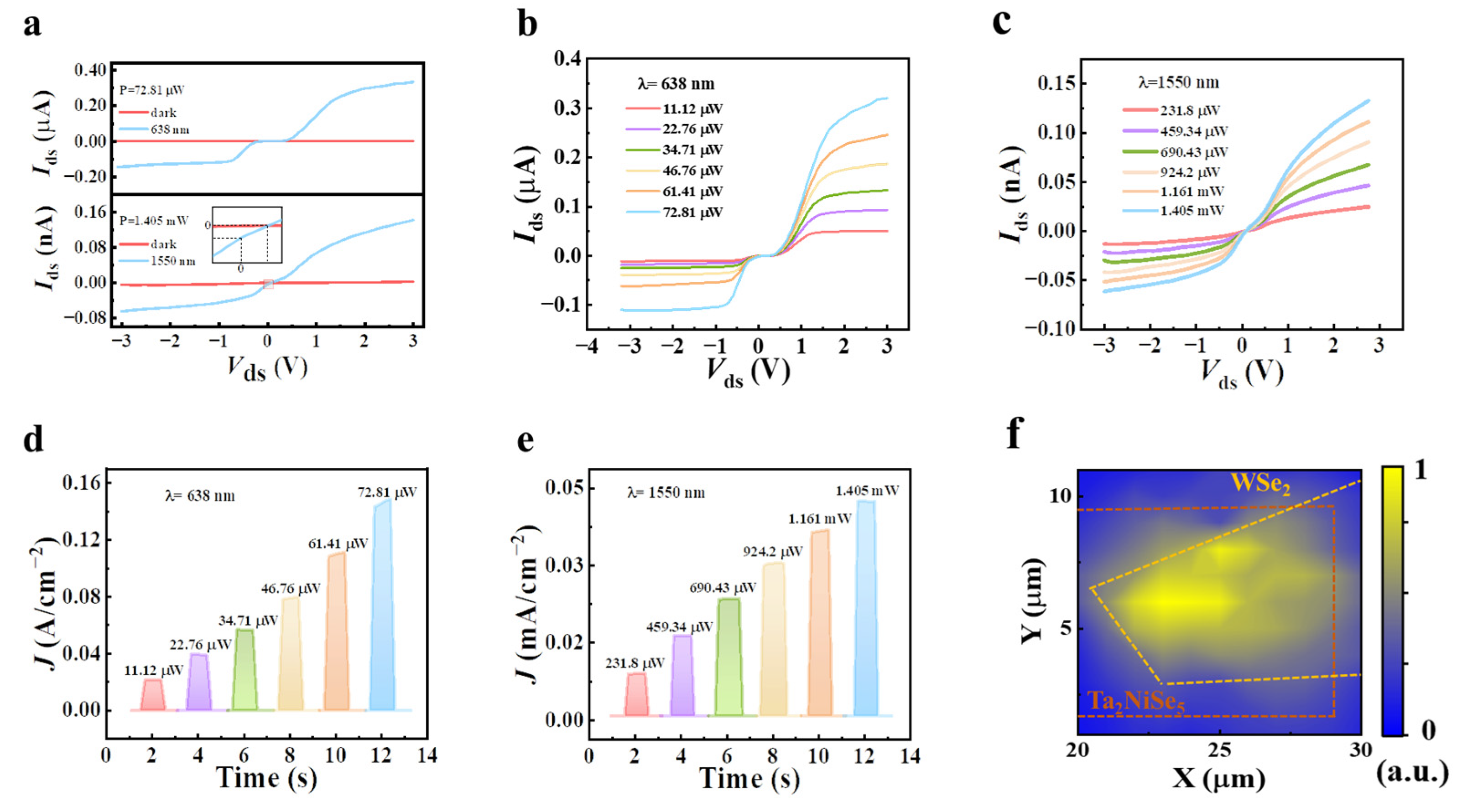
3. Results and Discussion
4. Conclusions
Author Contributions
Funding
Institutional Review Board Statement
Informed Consent Statement
Data Availability Statement
Conflicts of Interest
References
- Wang, H.; Kim, D.H. Perovskite-based photodetectors: Materials and devices. Chem. Soc. Rev. 2017, 46, 5204–5236. [Google Scholar] [CrossRef]
- Buscema, M.; Island, J.O.; Groenendijk, D.J.; Blanter, S.I.; Steele, G.A.; van der Zant, H.S.; Castellanos-Gomez, A. Photocurrent generation with two-dimensional van der Waals semiconductors. Chem. Soc. Rev. 2015, 44, 3691–3718. [Google Scholar] [CrossRef] [PubMed]
- Cheng, Z.; Zhao, T.; Zeng, H. 2D Material-Based Photodetectors for Infrared Imaging. Small Sci. 2021, 2, 2100051. [Google Scholar] [CrossRef]
- Wang, B.; Zhong, S.P.; Zhang, Z.B.; Zheng, Z.Q.; Zhang, Y.P.; Zhang, H. Broadband photodetectors based on 2D group IVA metal chalcogenides semiconductors. Appl. Mater. Today 2019, 15, 115–138. [Google Scholar] [CrossRef]
- Sun, B.; Shi, T.; Liu, Z.; Wu, Y.; Zhou, J.; Liao, G. Large-area flexible photodetector based on atomically thin MoS2/graphene film. Mater. Des. 2018, 154, 1–7. [Google Scholar] [CrossRef]
- Margalit, N.; Xiang, C.; Bowers, S.M.; Bjorlin, A.; Blum, R.; Bowers, J.E. Perspective on the future of silicon photonics and electronics. Appl. Phys. Lett. 2021, 118, 220501. [Google Scholar] [CrossRef]
- Wu, H.; Sun, Y.; Lin, D.; Zhang, R.; Zhang, C.; Pan, W. GaN Nanofibers based on Electrospinning: Facile Synthesis, Controlled Assembly, Precise Doping, and Application as High Performance UV Photodetector. Adv. Mater. 2009, 21, 227–231. [Google Scholar] [CrossRef]
- Li, D.; Sun, X.; Song, H.; Li, Z.; Chen, Y.; Jiang, H.; Miao, G. Realization of a high-performance GaN UV detector by nanoplasmonic enhancement. Adv. Mater. 2012, 24, 845–849. [Google Scholar] [CrossRef]
- Monroy, E.; Omnes, F.; Calle, F. Wide-bandgap semiconductor ultraviolet photodetectors. Semicond. Sci. Technol. 2003, 18, R33–R51. [Google Scholar] [CrossRef]
- Long, M.; Wang, P.; Fang, H.; Hu, W. Progress, Challenges, and Opportunities for 2D Material Based Photodetectors. Adv. Funct. Mater. 2018, 29, 1803807. [Google Scholar] [CrossRef]
- Wang, G.; Zhang, Y.; You, C.; Liu, B.; Yang, Y.; Li, H.; Cui, A.; Liu, D.; Yan, H. Two dimensional materials based photodetectors. Infrared Phys. Technol. 2018, 88, 149–173. [Google Scholar] [CrossRef]
- Fang, J.; Zhou, Z.; Xiao, M.; Lou, Z.; Wei, Z.; Shen, G. Recent advances in low-dimensional semiconductor nanomaterials and their applications in high-performance photodetectors. InfoMat 2019, 2, 291–317. [Google Scholar] [CrossRef]
- Fang, Y.; Armin, A.; Meredith, P.; Huang, J. Accurate characterization of next-generation thin-film photodetectors. Nat. Photonics 2018, 13, 1–4. [Google Scholar] [CrossRef]
- Yin, J.; Tan, Z.; Hong, H.; Wu, J.; Yuan, H.; Liu, Y.; Chen, C.; Tan, C.; Yao, F.; Li, T.; et al. Ultrafast and highly sensitive infrared photodetectors based on two-dimensional oxyselenide crystals. Nat. Commun. 2018, 9, 3311. [Google Scholar] [CrossRef]
- Wang, J.; Han, J.; Chen, X.; Wang, X. Design strategies for two-dimensional material photodetectors to enhance device performance. InfoMat 2019, 1, 33–53. [Google Scholar] [CrossRef]
- Abderrahmane, A.; Woo, C.; Ko, P.-J. Low Power Consumption Gate-Tunable WSe2/SnSe2 van der Waals Tunnel Field-Effect Transistor. Electronics 2022, 11, 833. [Google Scholar] [CrossRef]
- Shi, Z.; Zhang, H.; Khan, K.; Cao, R.; Zhang, Y.; Ma, C.; Tareen, A.K.; Jiang, Y.; Jin, M.; Zhang, H. Two-dimensional materials toward Terahertz optoelectronic device applications. J. Photochem. Photobiol. C Photochem. Rev. 2022, 51, 100473. [Google Scholar] [CrossRef]
- Xu, M.; Liang, T.; Shi, M.; Chen, H. Graphene-like two-dimensional materials. Chem. Rev. 2013, 113, 3766–3798. [Google Scholar] [CrossRef]
- Yin, Z.Y.; Li, H.; Li, H.; Jiang, L.; Shi, Y.M.; Sun, Y.H.; Lu, G.; Zhang, Q.; Chen, X.D.; Zhang, H. Single-Layer MoS2 Phototransistors. ACS Nano 2012, 6, 74–80. [Google Scholar] [CrossRef] [PubMed]
- Schneider, D.S.; Grundmann, A.; Bablich, A.; Passi, V.; Kataria, S.; Kalisch, H.; Heuken, M.; Vescan, A.; Neumaier, D.; Lemme, M.C. Highly Responsive Flexible Photodetectors Based on MOVPE Grown Uniform Few-Layer MoS2. ACS Photonics 2020, 7, 1388–1395. [Google Scholar] [CrossRef]
- Choi, W.; Cho, M.Y.; Konar, A.; Lee, J.H.; Cha, G.B.; Hong, S.C.; Kim, S.; Kim, J.; Jena, D.; Joo, J.; et al. High-detectivity multilayer MoS(2) phototransistors with spectral response from ultraviolet to infrared. Adv. Mater. 2012, 24, 5832–5836. [Google Scholar] [CrossRef]
- Lopez-Sanchez, O.; Lembke, D.; Kayci, M.; Radenovic, A.; Kis, A. Ultrasensitive photodetectors based on monolayer MoS2. Nat. Nanotechnol. 2013, 8, 497–501. [Google Scholar] [CrossRef] [PubMed]
- Das, S.; Zhang, W.; Demarteau, M.; Hoffmann, A.; Dubey, M.; Roelofs, A. Tunable transport gap in phosphorene. Nano Lett. 2014, 14, 5733–5739. [Google Scholar] [CrossRef]
- Avsar, A.; Tan, J.Y.; Kurpas, M.; Gmitra, M.; Watanabe, K.; Taniguchi, T.; Fabian, J.; Özyilmaz, B. Gate-tunable black phosphorus spin valve with nanosecond spin lifetimes. Nat. Phys. 2017, 13, 888–893. [Google Scholar] [CrossRef]
- Chen, X.; Wu, Y.; Wu, Z.; Han, Y.; Xu, S.; Wang, L.; Ye, W.; Han, T.; He, Y.; Cai, Y.; et al. High-quality sandwiched black phosphorus heterostructure and its quantum oscillations. Nat. Commun. 2015, 6, 7315. [Google Scholar] [CrossRef]
- Xu, Y.; Shi, X.; Zhang, Y.; Zhang, H.; Zhang, Q.; Huang, Z.; Xu, X.; Guo, J.; Zhang, H.; Sun, L.; et al. Epitaxial nucleation and lateral growth of high-crystalline black phosphorus films on silicon. Nat. Commun. 2020, 11, 1330. [Google Scholar] [CrossRef]
- Li, H.; Zhang, K.; Li, X.; Liu, B.; Li, L.; Mei, Z.; Chen, T.; Liu, Q.; Yu, W.; Yuan, J.; et al. Two-dimensional (2D) α-In2Se3/Ta2NiSe5 heterojunction photodetector with high sensitivity and fast response in a wide spectral range. Mater. Des. 2023, 227, 111799. [Google Scholar] [CrossRef]
- Guo, T.; Sa, Z.; Wei, P.; Jian, Y.; Chen, X.; Chen, Z.; Avila, J.; Dudin, P.; Yang, Z.-x.; Song, X.; et al. High-performance flexible broadband photodetectors enabled by 2D Ta2NiSe5 nanosheets. 2D Mater. 2023, 10, 025004. [Google Scholar] [CrossRef]
- Wakisaka, Y.; Sudayama, T.; Takubo, K.; Mizokawa, T.; Arita, M.; Namatame, H.; Taniguchi, M.; Katayama, N.; Nohara, M.; Takagi, H. Excitonic insulator state in Ta2NiSe5 probed by photoemission spectroscopy. Phys. Rev. Lett. 2009, 103, 026402. [Google Scholar] [CrossRef] [PubMed]
- Lu, Y.F.; Kono, H.; Larkin, T.I.; Rost, A.W.; Takayama, T.; Boris, A.V.; Keimer, B.; Takagi, H. Zero-gap semiconductor to excitonic insulator transition in Ta2NiSe5. Nat. Commun. 2017, 8, 14408. [Google Scholar] [CrossRef] [PubMed]
- Li, L.; Wang, W.; Gan, L.; Zhou, N.; Zhu, X.; Zhang, Q.; Li, H.; Tian, M.; Zhai, T. Ternary Ta2NiSe5 Flakes for a High-Performance Infrared Photodetector. Adv. Funct. Mater. 2016, 26, 8281–8289. [Google Scholar] [CrossRef]
- Zhang, Y.; Yu, W.; Li, J.; Chen, J.; Dong, Z.; Xie, L.; Li, C.; Shi, X.; Guo, W.; Lin, S.; et al. Ultra-broadband photodetection based on two-dimensional layered Ta2NiSe5 with strong anisotropy and high responsivity. Mater. Des. 2021, 208, 109894. [Google Scholar] [CrossRef]
- Qiao, J.; Feng, F.; Wang, Z.; Shen, M.; Zhang, G.; Yuan, X.; Somekh, M.G. Highly In-Plane Anisotropic Two-Dimensional Ternary Ta2NiSe5 for Polarization-Sensitive Photodetectors. ACS Appl. Mater. Interfaces 2021, 13, 17948–17956. [Google Scholar] [CrossRef] [PubMed]
- Wu, D.; Wang, Y.E.; Zeng, L.H.; Jia, C.; Wu, E.P.; Xu, T.T.; Shi, Z.F.; Tian, Y.T.; Li, X.J.; Tsang, Y.H. Design of 2D Layered PtSe2 Heterojunction for the High-Performance, Room-Temperature, Broadband, Infrared Photodetector. ACS Photonics 2018, 5, 3820–3827. [Google Scholar] [CrossRef]
- Wu, E.; Wu, D.; Jia, C.; Wang, Y.; Yuan, H.; Zeng, L.; Xu, T.; Shi, Z.; Tian, Y.; Li, X. In Situ Fabrication of 2D WS2/Si Type-II Heterojunction for Self-Powered Broadband Photodetector with Response up to Mid-Infrared. ACS Photonics 2019, 6, 565–572. [Google Scholar] [CrossRef]
- Chang, K.E.; Kim, C.; Yoo, T.J.; Kwon, M.G.; Heo, S.; Kim, S.Y.; Hyun, Y.; Yoo, J.I.; Ko, H.C.; Lee, B.H. High-Responsivity Near-Infrared Photodetector Using Gate-Modulated Graphene/Germanium Schottky Junction. Adv. Electron. Mater. 2019, 5, 1800957. [Google Scholar] [CrossRef]
- Yan, J.; Xiao, R.C.; Luo, X.; Lv, H.Y.; Zhang, R.R.; Sun, Y.; Tong, P.; Lu, W.J.; Song, W.H.; Zhu, X.B.; et al. Strong Electron-Phonon Coupling in the Excitonic Insulator Ta2NiSe5. Inorg. Chem. 2019, 58, 9036–9042. [Google Scholar] [CrossRef]
- Li, H.; Wu, J.M.T.; Yin, Z.Y.; Zhang, H. Preparation and Applications of Mechanically Exfoliated Single-Layer and Multi layer MoS2 and WSe2 Nanosheets. Acc. Chem. Res. 2014, 47, 1067–1075. [Google Scholar] [CrossRef]
- Mohammed, A.; Nakamura, H.; Wochner, P.; Ibrahimkutty, S.; Schulz, A.; Muller, K.; Starke, U.; Stuhlhofer, B.; Cristiani, G.; Logvenov, G.; et al. Pulsed laser deposition for the synthesis of monolayer WSe2. Appl. Phys. Lett. 2017, 111, 5. [Google Scholar] [CrossRef]
- Luo, H.; Wang, B.; Wang, E.; Wang, X.; Sun, Y.; Li, Q.; Fan, S.; Cheng, C.; Liu, K. Phase-transition modulated, high-performance dual-mode photodetectors based on WSe2/VO2 heterojunctions. Appl. Phys. Rev. 2019, 6, 041407. [Google Scholar] [CrossRef]
- Kang, J.; Tongay, S.; Zhou, J.; Li, J.; Wu, J. Band offsets and heterostructures of two-dimensional semiconductors. Appl. Phys. Lett. 2013, 102, 012111. [Google Scholar] [CrossRef]
- Zheng, Z.; Zhang, T.; Yao, J.; Zhang, Y.; Xu, J.; Yang, G. Flexible, transparent and ultra-broadband photodetector based on large-area WSe2 film for wearable devices. Nanotechnology 2016, 27, 225501. [Google Scholar] [CrossRef] [PubMed]
- Lu, J.; Carvalho, A.; Liu, H.; Lim, S.X.; Castro Neto, A.H.; Sow, C.H. Hybrid Bilayer WSe2 -CH3 NH3 PbI3 Organolead Halide Perovskite as a High-Performance Photodetector. Angew. Chem. Int. Ed. Engl. 2016, 55, 11945–11949. [Google Scholar] [CrossRef]
- Qiao, J.; Feng, F.; Song, S.; Wang, T.; Shen, M.; Zhang, G.; Yuan, X.; Somekh, M.G. Perovskite Quantum Dot-Ta2NiSe5 Mixed-Dimensional Van Der Waals Heterostructures for High-Performance Near-Infrared Photodetection. Adv. Funct. Mater. 2021, 32, 2110706. [Google Scholar] [CrossRef]
- Schlaf, R.; Lang, O.; Pettenkofer, C.; Jaegermann, W. Band lineup of layered semiconductor heterointerfaces prepared by van der Waals epitaxy: Charge transfer correction term for the electron affinity rule. J. Appl. Phys. 1999, 85, 2732–2753. [Google Scholar] [CrossRef]
- Wu, Z.; Jie, W.; Yang, Z.; Hao, J. Hybrid heterostructures and devices based on two-dimensional layers and wide bandgap materials. Mater. Today Nano 2020, 12, 100092. [Google Scholar] [CrossRef]
- Yang, J.; Yu, W.; Pan, Z.; Yu, Q.; Yin, Q.; Guo, L.; Zhao, Y.; Sun, T.; Bao, Q.; Zhang, K. Ultra-Broadband Flexible Photodetector Based on Topological Crystalline Insulator SnTe with High Responsivity. Small 2018, 14, e1802598. [Google Scholar] [CrossRef] [PubMed]
- Guo, C.; Liu, C.; Zhang, S.; Shi, C.; Chen, Z.; Yu, X.; Chen, X. Ultrafast visible-infrared photodetector based on the SnSe2/Bi2Se3 heterostructure. Opt. Lett. 2022, 47, 4977–4980. [Google Scholar] [CrossRef]
- Lu, X.W.; Sun, L.; Jiang, P.; Bao, X.H. Progress of Photodetectors Based on the Photothermoelectric Effect. Adv. Mater. 2019, 31, 26. [Google Scholar] [CrossRef] [PubMed]
- Zhang, Y.; Huang, L.; Li, J.; Dong, Z.; Yu, Q.; Lei, T.; Chen, C.; Yang, L.; Dai, Y.; Zhang, J.; et al. Two-dimensional Ta2NiSe5/GaSe van der Waals heterojunction for ultrasensitive visible and near-infrared dual-band photodetector. Appl. Phys. Lett. 2022, 120, 261101. [Google Scholar] [CrossRef]
- Guo, T.; Song, X.; Wei, P.; Li, J.; Gao, Y.; Cheng, Z.; Zhou, W.; Gu, Y.; Chen, X.; Zeng, H.; et al. High-Gain MoS2/Ta2NiSe5 Heterojunction Photodetectors with Charge Transfer and Suppressing Dark Current. ACS Appl. Mater. Interfaces 2022, 14, 56384–56394. [Google Scholar] [CrossRef] [PubMed]
- Kapatel, S.; Sumesh, C.K. Atomically thin WSe2 nanosheets for fabrication of high-performance p-Si/WSe2 heterostructure. Opt. Mater. 2022, 129, 112537. [Google Scholar] [CrossRef]
- Gao, W.; Zhang, F.; Zheng, Z.; Li, J. Unique and Tunable Photodetecting Performance for Two-Dimensional Layered MoSe2/WSe2 p–n Junction on the 4H-SiC Substrate. ACS Appl. Mater. Interfaces 2019, 11, 19277–19285. [Google Scholar] [CrossRef] [PubMed]
- Kang, X.; Lan, C.; Li, F.; Wang, W.; Yip, S.; Meng, Y.; Wang, F.; Lai, Z.; Liu, C.; Ho, J.C. Van der Waals PdSe2/WS2 Heterostructures for Robust High-Performance Broadband Photodetection from Visible to Infrared Optical Communication Band. Adv. Opt. Mater. 2021, 9, 2001991. [Google Scholar] [CrossRef]


| Materials | Wavelength Range (nm) | Dark Current | Rise/Decay Time | On/Off | Reference |
|---|---|---|---|---|---|
| Ta2NiSe5/WSe2 | 638/1550 | ~3.6 pA | 278/283 μs | ~104 | This work |
| Ta2NiSe5/GaSe | 520/1550 | ~4 pA | 340/32 ms | 5 × 10³ | [50] |
| Ta2NiSe5/MoS2 | 532/1064 | ~11 pA | 7.4/31.1 s | 1.9 × 10² | [51] |
| WSe2/Si | 670 | - | 75/125 ms | 3.2 | [52] |
| WSe2/MoSe2 | 532 | ~0.078 nA | 4.3/22.6 ms | ~103 | [53] |
| PdSe2/Si | 532/1550 | ~10 pA | 49/90 ms | ~103 | [54] |
Disclaimer/Publisher’s Note: The statements, opinions and data contained in all publications are solely those of the individual author(s) and contributor(s) and not of MDPI and/or the editor(s). MDPI and/or the editor(s) disclaim responsibility for any injury to people or property resulting from any ideas, methods, instructions or products referred to in the content. |
© 2023 by the authors. Licensee MDPI, Basel, Switzerland. This article is an open access article distributed under the terms and conditions of the Creative Commons Attribution (CC BY) license (https://creativecommons.org/licenses/by/4.0/).
Share and Cite
Xiao, P.; Zhang, S.; Zhang, L.; Yang, J.; Shi, C.; Han, L.; Tang, W.; Zhu, B. Visible Near-Infrared Photodetection Based on Ta2NiSe5/WSe2 van der Waals Heterostructures. Sensors 2023, 23, 4385. https://doi.org/10.3390/s23094385
Xiao P, Zhang S, Zhang L, Yang J, Shi C, Han L, Tang W, Zhu B. Visible Near-Infrared Photodetection Based on Ta2NiSe5/WSe2 van der Waals Heterostructures. Sensors. 2023; 23(9):4385. https://doi.org/10.3390/s23094385
Chicago/Turabian StyleXiao, Pan, Shi Zhang, Libo Zhang, Jialiang Yang, Chaofan Shi, Li Han, Weiwei Tang, and Bairen Zhu. 2023. "Visible Near-Infrared Photodetection Based on Ta2NiSe5/WSe2 van der Waals Heterostructures" Sensors 23, no. 9: 4385. https://doi.org/10.3390/s23094385
APA StyleXiao, P., Zhang, S., Zhang, L., Yang, J., Shi, C., Han, L., Tang, W., & Zhu, B. (2023). Visible Near-Infrared Photodetection Based on Ta2NiSe5/WSe2 van der Waals Heterostructures. Sensors, 23(9), 4385. https://doi.org/10.3390/s23094385