
Design of Wideband High-Gain Patch Antenna Array for High-Temperature Applications


Abstract
:1. Introduction
2. Antenna Model and Design
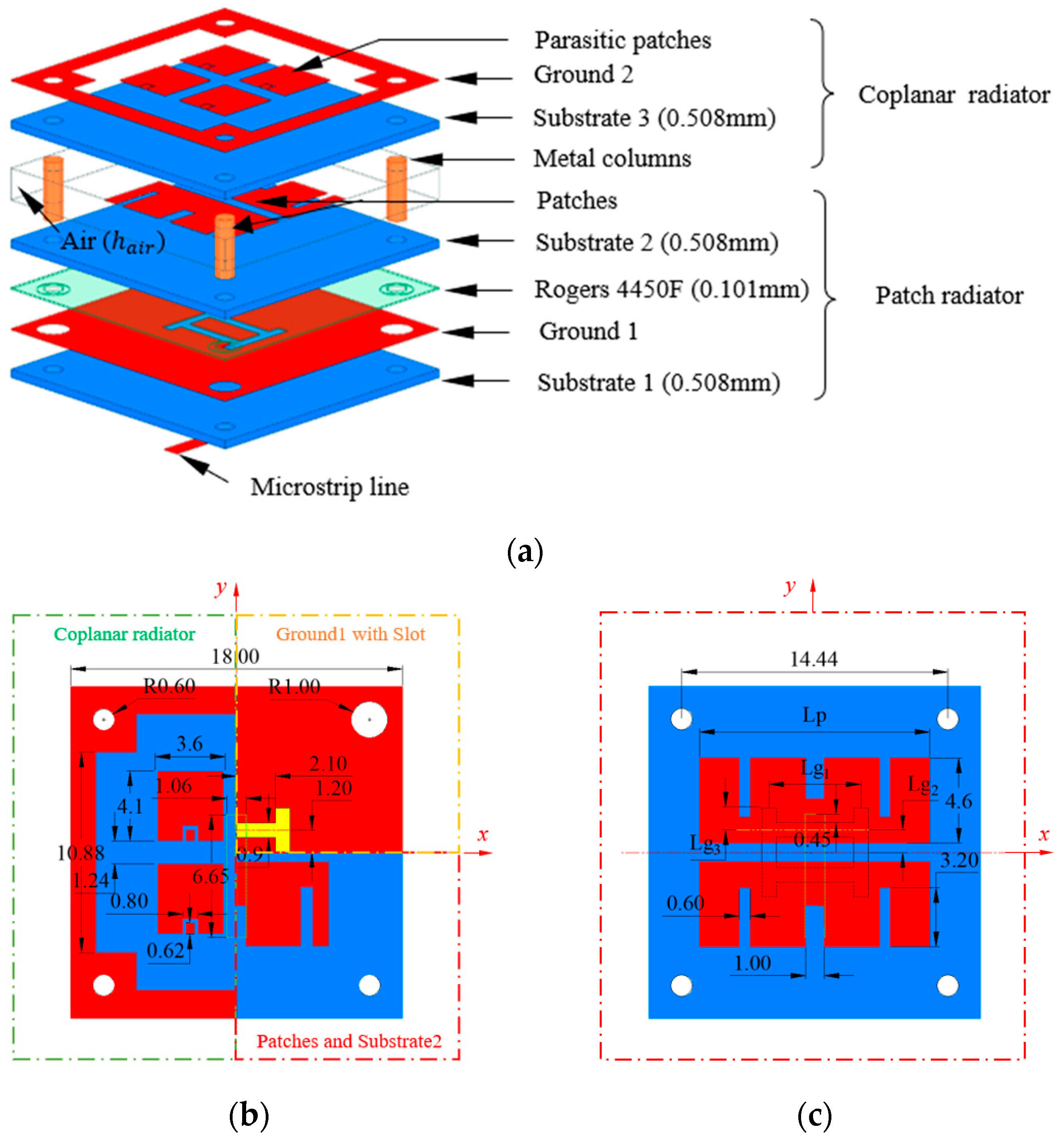
2.1. Antenna Element Geometry
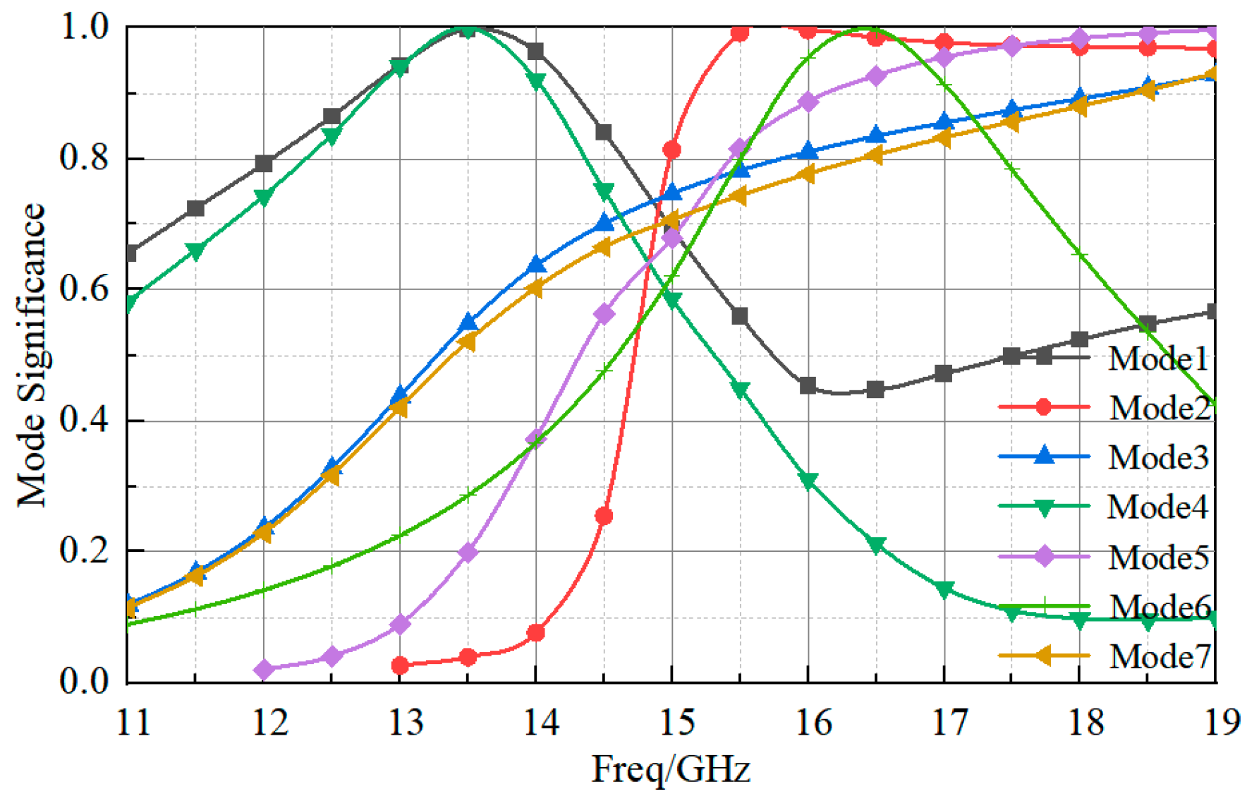
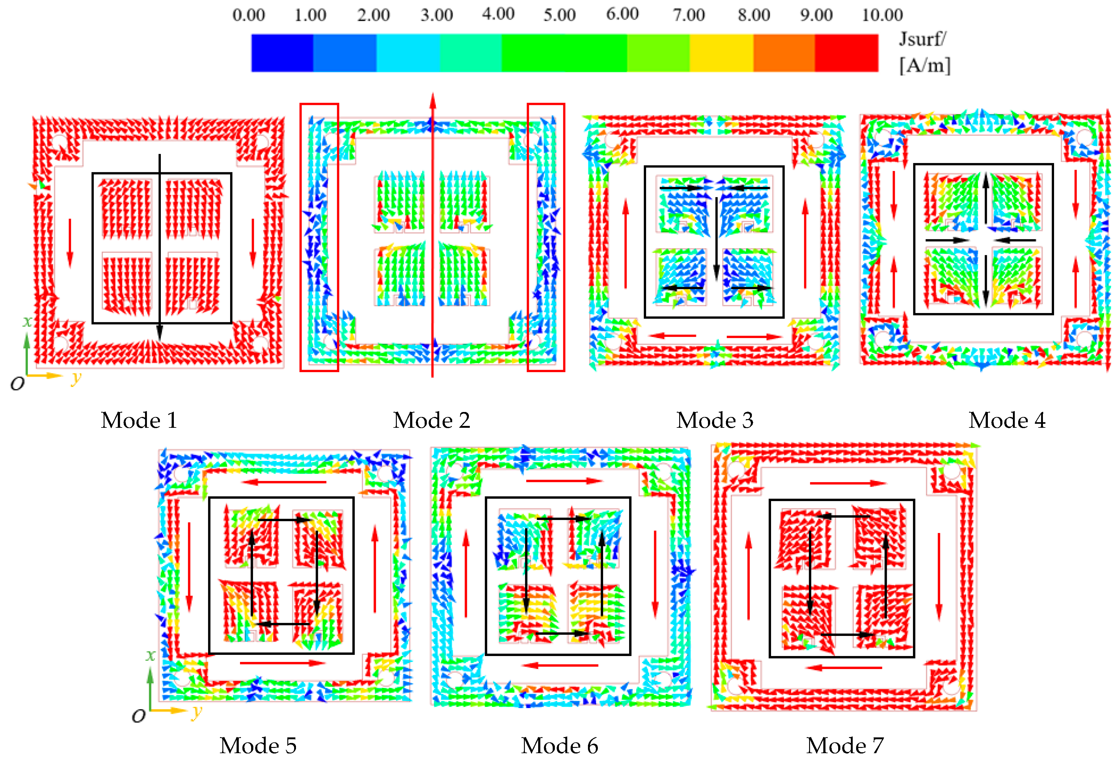
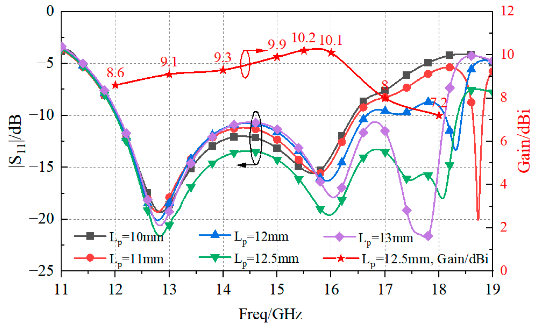
2.2. Antenna Element Design
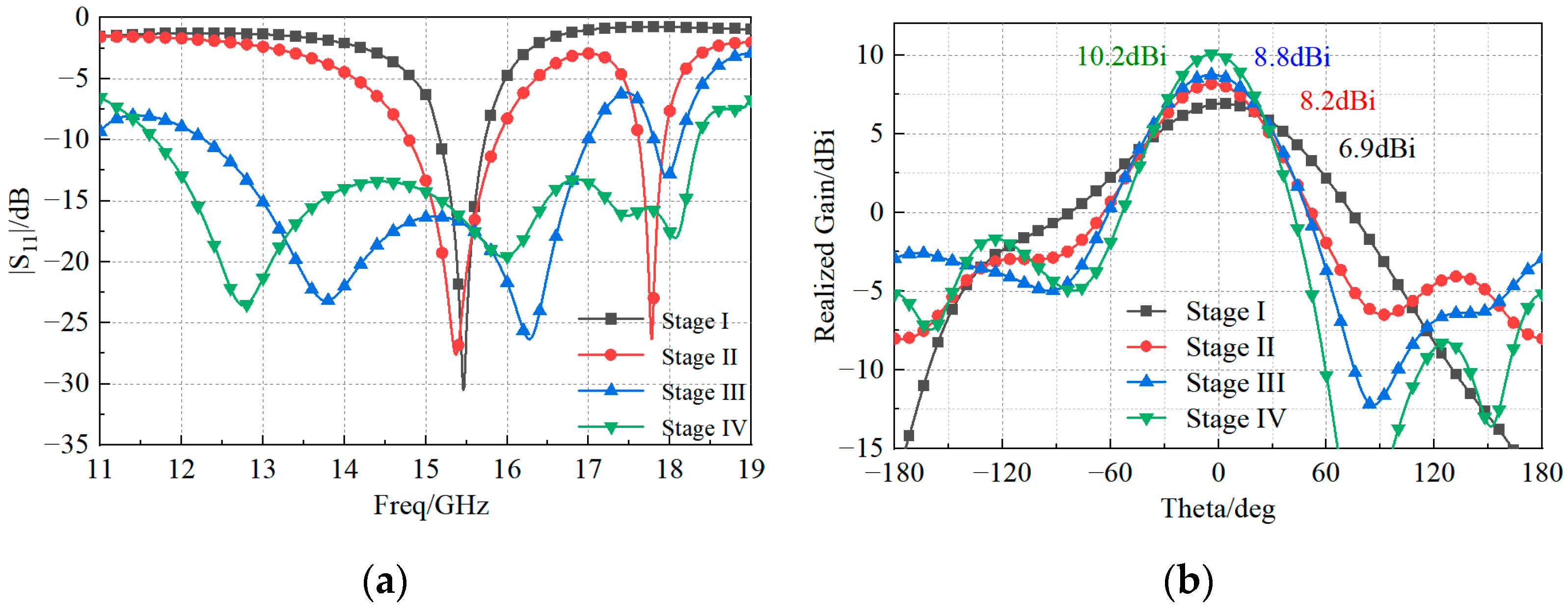
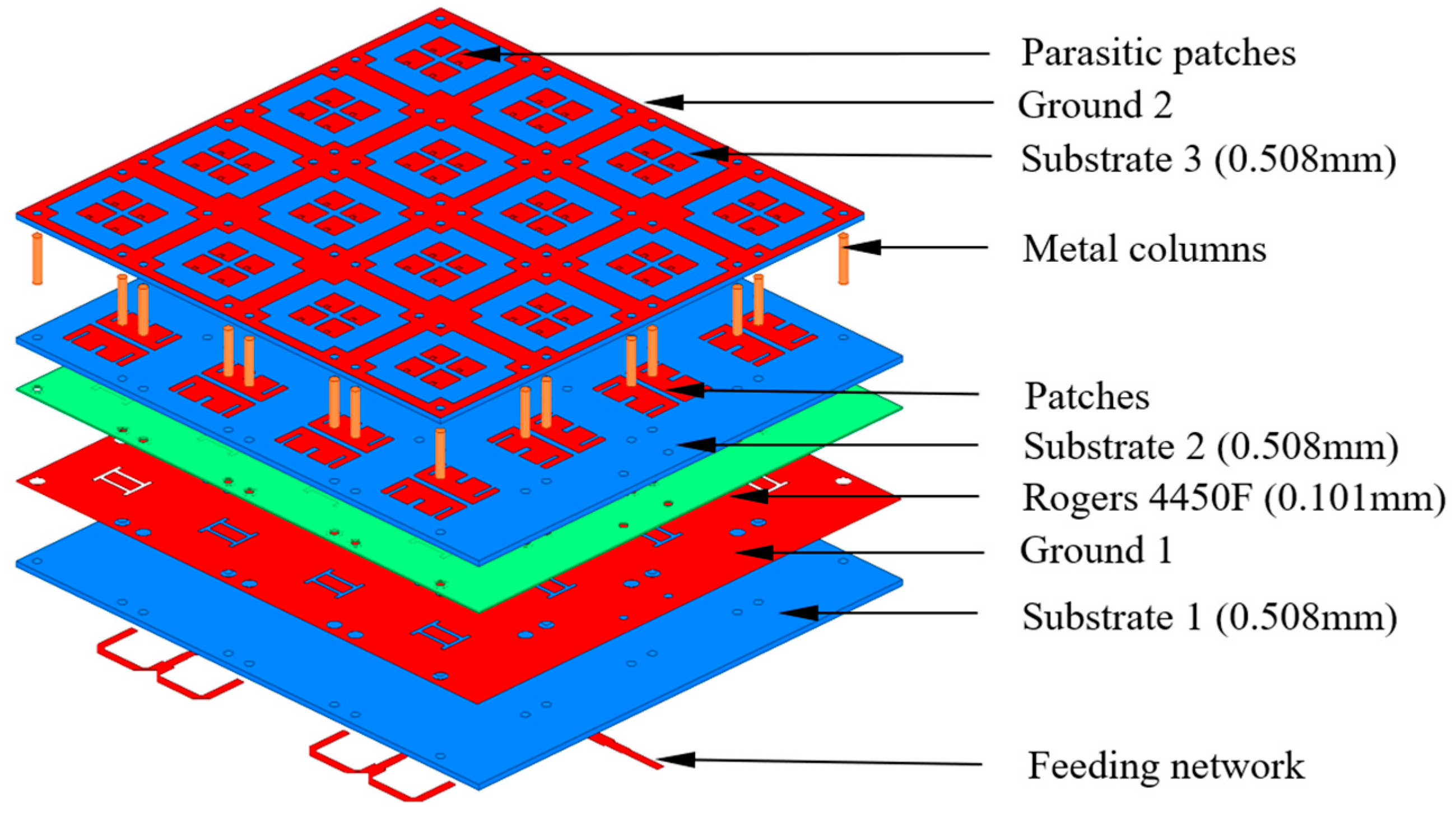
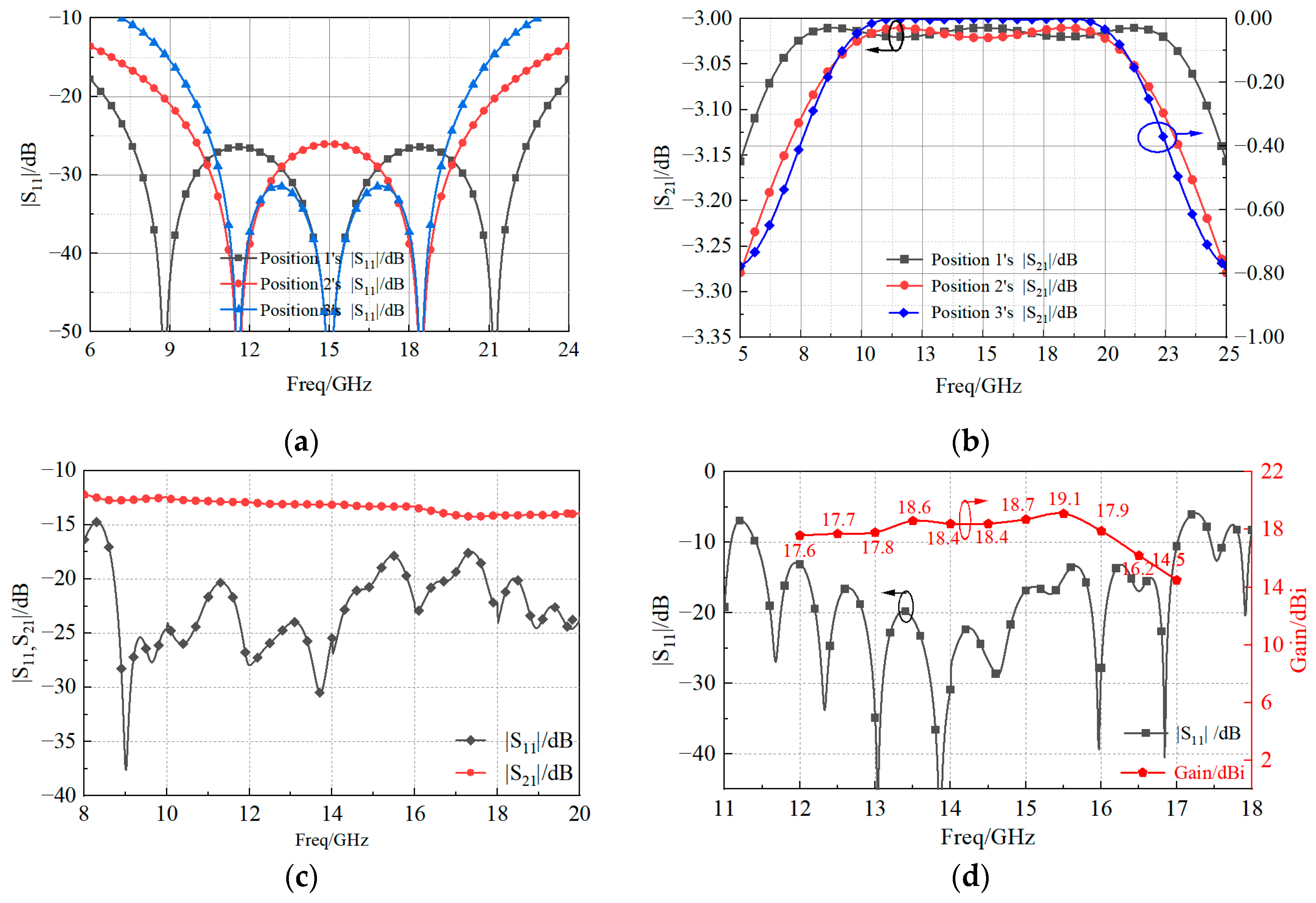
2.3. 4 × 4 Antenna Array Design
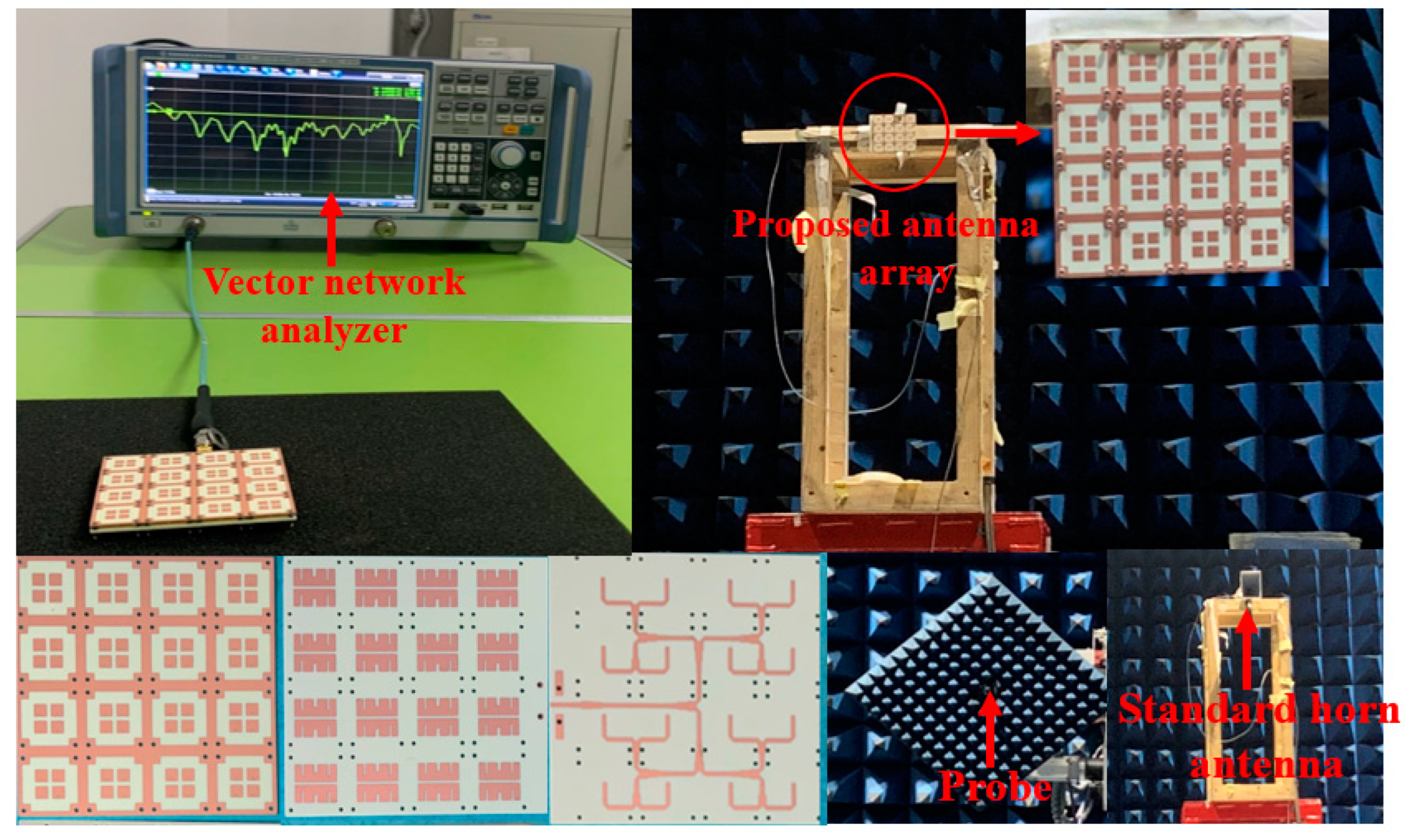
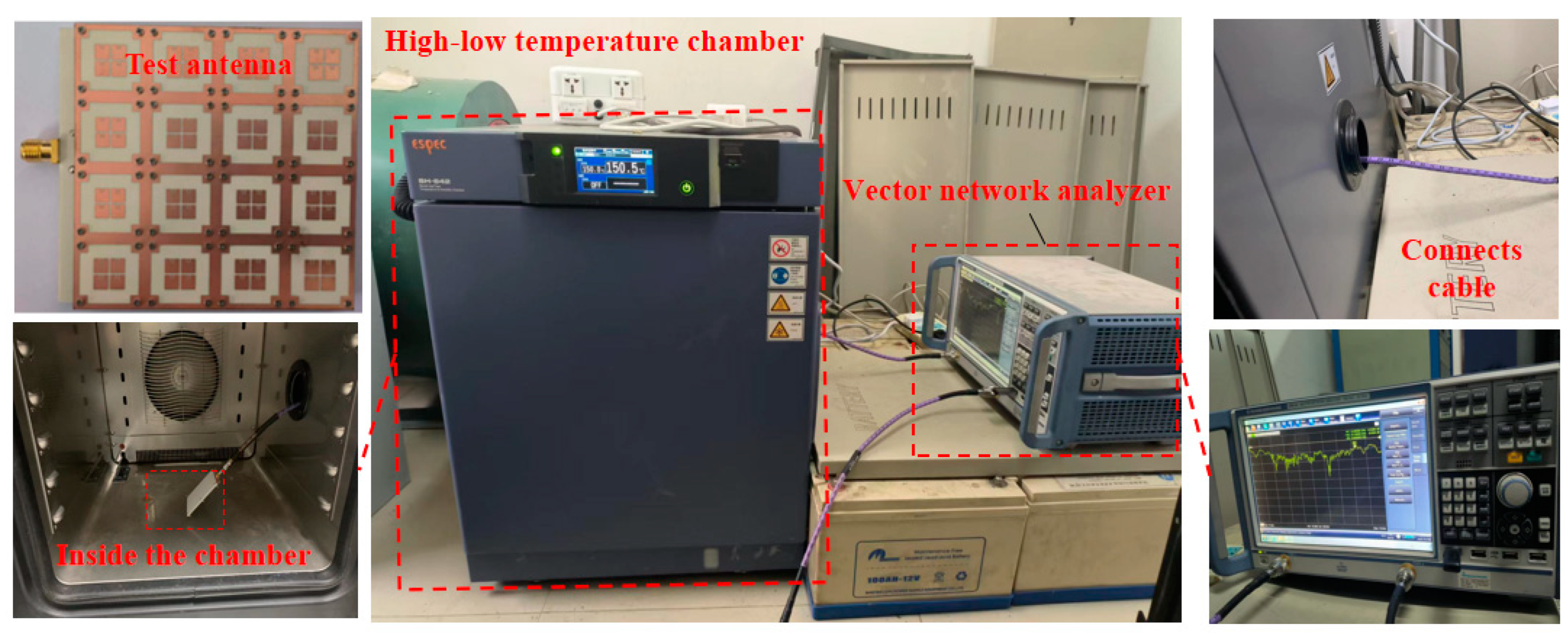
3. Experimental Measurements and Discussion
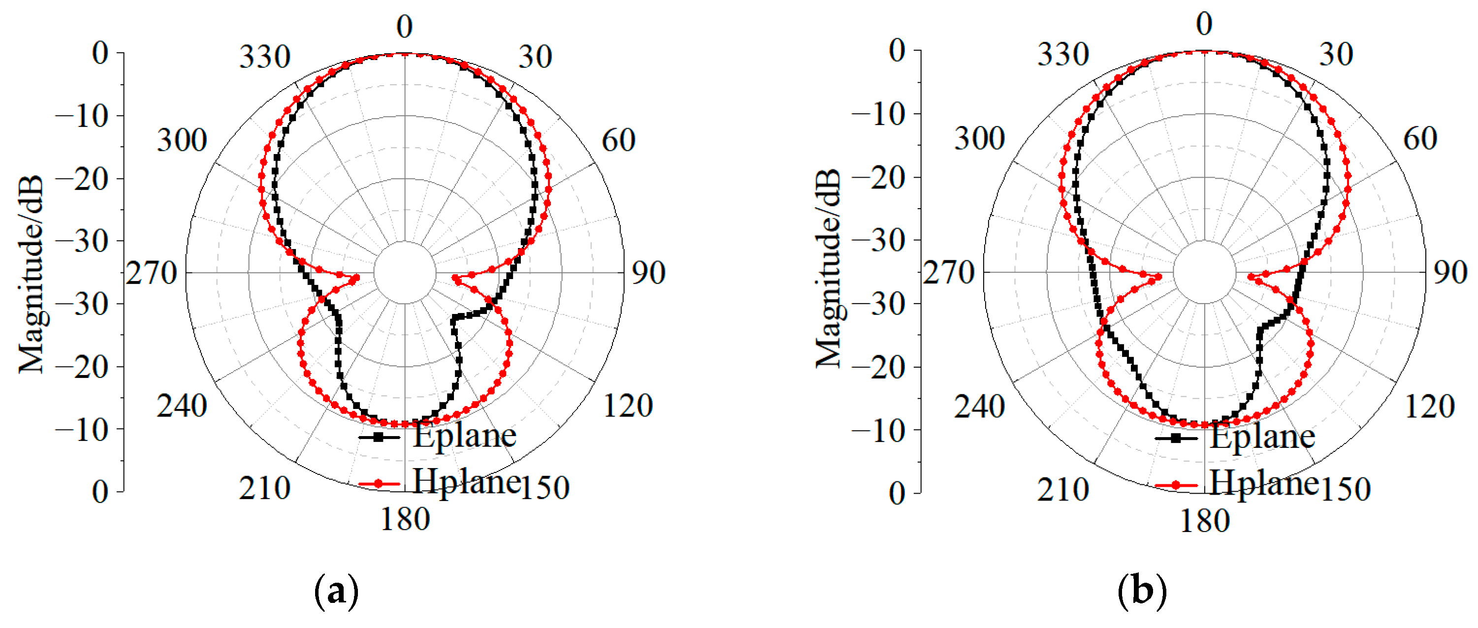
3.1. Measurement at Normal Temperature
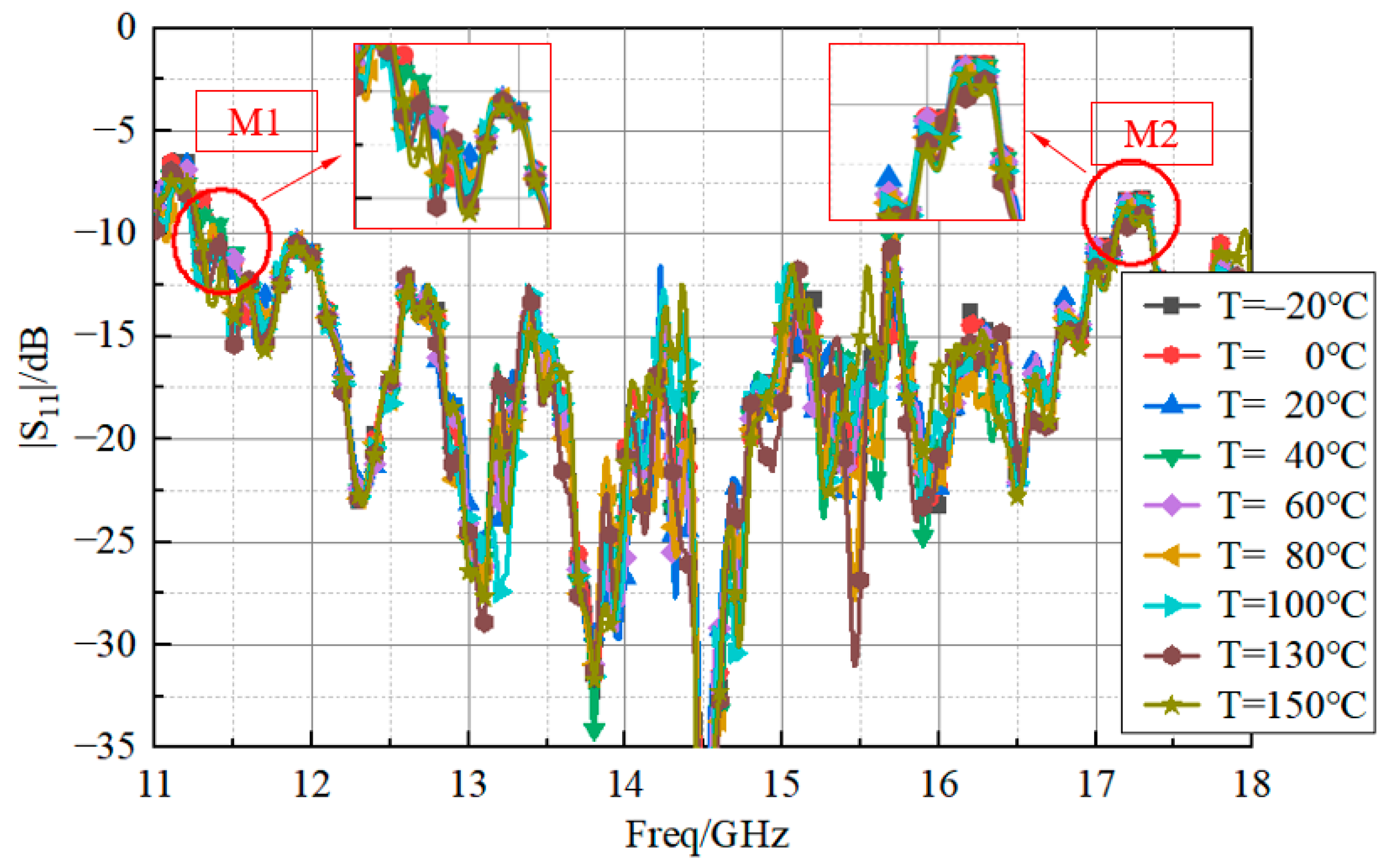
3.2. Measurement in High-Low Temperature Chamber
4. Conclusions
Author Contributions
Funding
Institutional Review Board Statement
Informed Consent Statement
Data Availability Statement
Conflicts of Interest
References
- Nagy, L. Microstrip Antenna Development for Radar Sensor. Sensors 2023, 23, 909. [Google Scholar] [CrossRef] [PubMed]
- Jain, P.; Chhabra, H.; Chauhan, U.; Prakash, K.; Gupta, A.; Soliman, M.S.; Islam, M.S.; Islam, M.T. Machine learning assisted hepta band THz metamaterial absorber for biomedical applications. Sci. Rep. 2023, 13, 1792. [Google Scholar] [CrossRef] [PubMed]
- Sheng, X.; Lu, X.; Liu, N.; Liu, Y. Design of Broadband High-Gain Fabry–Pérot Antenna Using Frequency-Selective Surface. Sensors 2022, 22, 9698. [Google Scholar] [CrossRef] [PubMed]
- Kim, S.-W.; Yu, H.-G.; Choi, D.-Y. Analysis of Patch Antenna with Broadband Using Octagon Parasitic Patch. Sensors 2021, 21, 4908. [Google Scholar] [CrossRef] [PubMed]
- Anim, K.; Danuor, P.; Park, S.-O.; Jung, Y.-B. High-Efficiency Broadband Planar Array Antenna with Suspended Microstrip Slab for X-Band SAR Onboard Small Satellites. Sensors 2022, 22, 252. [Google Scholar] [CrossRef]
- Ghimire, J.; Diba, F.D.; Kim, J.-H.; Choi, D.-Y. Vivaldi Antenna Arrays Feed by Frequency-Independent Phase Shifter for High Directivity and Gain Used in Microwave Sensing and Communication Applications. Sensors 2021, 21, 6091. [Google Scholar] [CrossRef]
- Hehenberger, S.P.; Elmarissi, W.; Caizzone, S. Design and Installed Performance Analysis of a Miniaturized All-GNSS Bands Antenna Array for Robust Navigation on UAV Platforms. Sensors 2022, 22, 9645. [Google Scholar] [CrossRef]
- Anim, K.; Lee, J.-N.; Jung, Y.-B. High-Gain Millimeter-Wave Patch Array Antenna for Unmanned Aerial Vehicle Application. Sensors 2021, 21, 3914. [Google Scholar] [CrossRef]
- Zhong, S.S. Microstrip Antenna Theory and Application; Xidian University Press: Xi’an, China, 1991. [Google Scholar]
- Li, P.; Wang, C.; Xu, W.; Song, L. Taylor Expansion and Matrix-Based Interval Analysis of Linear Arrays With Patch Element Pattern Tolerance. IEEE Access 2021, 9, 21004–21015. [Google Scholar] [CrossRef]
- Wang, C.; Li, P.; Xu, W.; Song, L.; Huang, J. Tolerance analysis of 3D printed patch antennas based on interval arithmetic. Microw. Opt. Technol. Lett. 2021, 63, 516–524. [Google Scholar] [CrossRef]
- Li, P.; Xu, W.Y.; Song, L.W. Power Pattern Tolerance Analysis of Radome with the Material Properties Error Based on Interval Arithmetic. IEEE Antennas Wirel. Propag. Lett. 2017, 16, 1321–1324. [Google Scholar] [CrossRef]
- Matin, M.; Sharif, B.; Tsimenidis, C. Probe-fed stacked patch antenna for wideband applications. IEEE Trans. Antennas Propag. 2007, 55, 2385–2388. [Google Scholar] [CrossRef]
- Sung, Y. Bandwidth enhancement of a microstrip line-fed printed wide slot antenna with a parasitic center patch. IEEE Trans. Antennas Propag. 2012, 60, 1712–1716. [Google Scholar] [CrossRef]
- Wi, S.; Lee, Y.; Yook, J. Wideband microstrip patch antenna with U shaped parasitic elements. IEEE Trans. Antennas Propag. 2007, 55, 1196–1199. [Google Scholar] [CrossRef]
- Lee, K.; Luk, K.; Tong, K.; Shum, S.; Huynh, T.; Lee, R. Experimental and simulation studies of the coaxially fed U-slot rectangular patch antenna. IEE Proc. Microw. Antennas Propag. 1997, 144, 354–358. [Google Scholar] [CrossRef]
- Khidre, A.; Lee, K.; Elsherbeni, A.Z.; Yang, F. Wide band dualbeamU-slot microstrip antenna. IEEE Trans. Antennas Propag. 2013, 61, 1415–1418. [Google Scholar] [CrossRef]
- Liu, W.; Yin, Y.; Xu, W.; Zuo, S. Compact open-slot antenna with bandwidth enhancement. IEEE Antennas Wirel. Propag. Lett. 2011, 10, 850–853. [Google Scholar]
- Salucci, M.; Robol, F.; Anselmi, N.; Hannan, M.A.; Rocca, P.; Oliveri, G.; Donelli, M.; Massa, A. S-Band spline-shaped aperture-stacked patch antenna for air traffic control applications. IEEE Trans. Antennas Propag. 2018, 66, 4292–4297. [Google Scholar] [CrossRef]
- Massa, A.; Salucci, M. On the design of complex EM devices and systems through the system-by-design paradigm—A framework for dealing with the computational complexity. IEEE Trans. Antennas Propag. 2018, 70, 1328–1343. [Google Scholar] [CrossRef]
- Ou, J.-H.; Huang, J.; Liu, J.; Tang, J.; Zhang, X.Y. High-Gain Circular Patch Antenna and Array with Introduction of Multiple Shorting Pins. IEEE Trans. Antennas Propag. 2020, 68, 6506–6515. [Google Scholar] [CrossRef]
- Liu, Z.; Zhu, L.; Zhang, X. A Low-Profile and High-Gain CP Patch Antenna with Improved AR Bandwidth Via Perturbed Ring Resonator. IEEE Antennas Wirel. Propag. Lett. 2019, 18, 397–401. [Google Scholar] [CrossRef]
- Zhang, X.; Hong, K.-D.; Zhu, L.; Bi, X.-K.; Yuan, T. Wideband Differentially Fed Patch Antennas Under Dual High-Order Modes for Stable High Gain. IEEE Trans. Antennas Propag. 2021, 69, 508–513. [Google Scholar] [CrossRef]
- Hong, K.-D.; Zhang, X.; Zhu, L.; Yuan, T. A High-Gain and Pattern-Reconfigurable Patch Antenna Under Operation of TM₂₀ and TM₂₁ Modes. IEEE Open J. Antennas Propag. 2021, 2, 646–653. [Google Scholar] [CrossRef]
- Luo, Y.; Chen, Z.N.; Ma, K. A Single-Layer Dual-Polarized Differentially Fed Patch Antenna with Enhanced Gain and Bandwidth Operating at Dual Compressed High-Order Modes Using Characteristic Mode Analysis. IEEE Trans. Antennas Propag. 2020, 68, 4082–4087. [Google Scholar] [CrossRef]
- Wang, X.; Tang, S.; Yang, L.; Chen, J. Differential-Fed Dual-Polarized Dielectric Patch Antenna with Gain Enhancement Based on Higher Order Modes. IEEE Antennas Wirel. Propag. Lett. 2020, 19, 502–506. [Google Scholar] [CrossRef]
- Zhang, X.; Tan, T.-Y.; Wu, Q.-S.; Zhu, L.; Zhong, S.; Yuan, T. Pin-Loaded Patch Antenna Fed with a Dual-Mode SIW Resonator for Bandwidth Enhancement and Stable High Gain. IEEE Antennas Wirel. Propag. Lett. 2021, 20, 279–283. [Google Scholar] [CrossRef]
- Yeap, S.; Chen, Z. Microstrip patch antennas with enhanced gain by partial substrate removal. IEEE Trans. Antennas Propag. 2010, 58, 2811–2816. [Google Scholar] [CrossRef]
- Bhattacharyya, A. Long rectangular patch antenna with a single feed. IEEE Trans. Antennas Propag. 1990, 38, 987–993. [Google Scholar] [CrossRef]
- Chin, C.; Xue, Q.; Chan, C. Design of a 5.8-GHz rectenna incorporating a new patch antenna. IEEE Antennas Wirel. Propag. Lett. 2005, 4, 175–178. [Google Scholar] [CrossRef]
- Wang, Z.; Liu, J.; Long, Y. A Simple Wide-Bandwidth and High-Gain Microstrip Patch Antenna with Both Sides Shorted. IEEE Antennas Wirel. Propag. Lett. 2019, 18, 1144–1148. [Google Scholar] [CrossRef]
- Wei, J.; Jiang, X.; Peng, L. Ultrawideband and High-Gain Circularly Polarized Antenna with Double-Y-Shape Slot. IEEE Antennas Wirel. Propag. Lett. 2017, 16, 1508–1511. [Google Scholar] [CrossRef]
- Zhou, Z.; Wei, Z.; Tang, Z.; Yin, Y. Design and Analysis of a Wideband Multiple-Microstrip Dipole Antenna with High Isolation. IEEE Antennas Wirel. Propag. Lett. 2019, 18, 722–726. [Google Scholar] [CrossRef]
- Pavuluri, S.K.; Wang, C.; Sangster, A.J. High Efficiency Wideband Aperture-Coupled Stacked Patch Antennas Assembled Using Millimeter Thick Micromachined Polymer Structures. IEEE Trans. Antennas Propag. 2010, 58, 3616–3621. [Google Scholar] [CrossRef]
- Dong, H.-J.; Kim, Y.-B.; Joung, J.; Lee, H.L. High Gain and Low-Profile Stacked Magneto-Electric Dipole Antenna for Phased Array Beamforming. IEEE Access 2020, 8, 180295–180304. [Google Scholar] [CrossRef]


| Ref | Dimensions | Permittivity | Bandwidth, FBW (GHz, %) | Peak Gain (dBi) | Number of Ports |
|---|---|---|---|---|---|
| [3] | 4.8 × 4.8 × 0.63 | 2.2 | 8.3–11.25, 29.5% | 10.4 | 1 |
| [4] | 1.48 × 1.48 × 0.04 | 3 | 8.17–9.61, 16.2% | 8.9 | 1 |
| [8] | 0.7 × 0.7 × 0.13 | 2.2 | 25.58–27.04, 5.2% | 7.8 | 1 |
| [13] | / | 1.1 | 3.27–6, 59.7% | 8 | 1 |
| [31] | 1.3 × 0.7 × 0.04 | 2.2 | 5.13–5.85, 13.1% | 9.7 | 1 |
| [32] | 0.4 × 0.4 × 0.23 | 2.65 | 3.6–6, 49.8% | 8.5 | 1 |
| [33] | 0.78 × 0.78 × 0.18 | 4.4 | 1.68–2.75, 48% | 8.9 | 2 |
| [34] | 0.5 × 0.5 × 0.25 | 3.2 | 6.5–10.2, 37% | 7.8 | 1 |
| [35] | 0.96 × 0.96 × 0.14 | 2.5 | 5.2–5.9, 12.6% | 9.6 | 1 |
| Present | 0.9 × 0.9 × 0.18 | 3.66 | 12–18.25, 41.3% | 10.2 | 1 |
| Temperature (°C) | M1 (GHz) | M2 (GHz) | Bandwidth (GHz) |
|---|---|---|---|
| −20 | 11.39 | 17.04 | 5.65 |
| 0 | 11.38 | 17.02 | 5.64 |
| 20 | 11.27 | 17.01 | 5.74 |
| 40 | 11.44 | 17.12 | 5.68 |
| 60 | 11.46 | 17.10 | 5.64 |
| 80 | 11.38 | 17.12 | 5.74 |
| 100 | 11.40 | 17.12 | 5.72 |
| 130 | 11.44 | 17.10 | 5.66 |
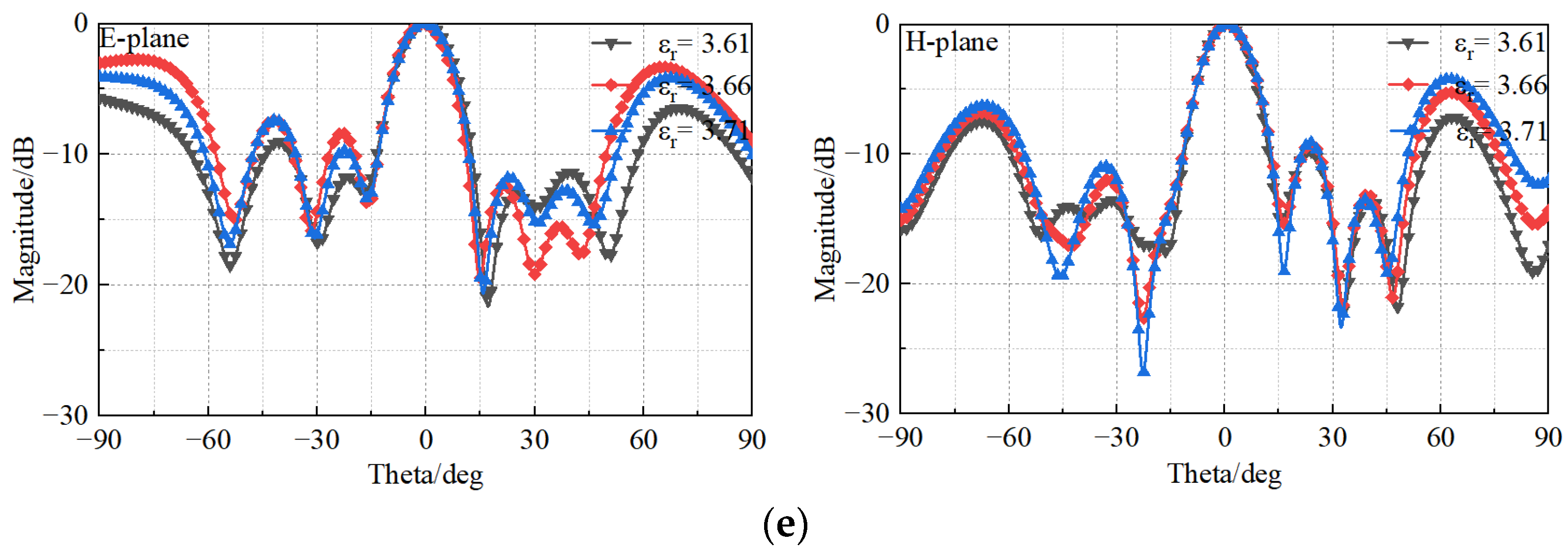
| Permittivity | M1 (GHz) | M2 (GHz) | Bandwidth (GHz) |
|---|---|---|---|
| 3.61 | 11.45 | 17.20 | 5.75 |
| 3.66 | 11.4 | 17 | 5.6 |
| 3.71 | 11.36 | 17 | 5.64 |
Disclaimer/Publisher’s Note: The statements, opinions and data contained in all publications are solely those of the individual author(s) and contributor(s) and not of MDPI and/or the editor(s). MDPI and/or the editor(s) disclaim responsibility for any injury to people or property resulting from any ideas, methods, instructions or products referred to in the content. |
© 2023 by the authors. Licensee MDPI, Basel, Switzerland. This article is an open access article distributed under the terms and conditions of the Creative Commons Attribution (CC BY) license (https://creativecommons.org/licenses/by/4.0/).
Share and Cite
Li, R.; Li, P.; Rocca, P.; Salas Sánchez, A.Á.; Song, L.; Li, X.; Xu, W.; Fan, Z. Design of Wideband High-Gain Patch Antenna Array for High-Temperature Applications. Sensors 2023, 23, 3821. https://doi.org/10.3390/s23083821
Li R, Li P, Rocca P, Salas Sánchez AÁ, Song L, Li X, Xu W, Fan Z. Design of Wideband High-Gain Patch Antenna Array for High-Temperature Applications. Sensors. 2023; 23(8):3821. https://doi.org/10.3390/s23083821
Chicago/Turabian StyleLi, Ruibo, Peng Li, Paolo Rocca, Aarón Ángel Salas Sánchez, Liwei Song, Xinghua Li, Wanye Xu, and Zijiao Fan. 2023. "Design of Wideband High-Gain Patch Antenna Array for High-Temperature Applications" Sensors 23, no. 8: 3821. https://doi.org/10.3390/s23083821
APA StyleLi, R., Li, P., Rocca, P., Salas Sánchez, A. Á., Song, L., Li, X., Xu, W., & Fan, Z. (2023). Design of Wideband High-Gain Patch Antenna Array for High-Temperature Applications. Sensors, 23(8), 3821. https://doi.org/10.3390/s23083821