Abstract
This paper presents a low-frequency shadow sinusoidal oscillator using a bulk-driven multiple-input operational transconductance amplifier (MI-OTA) with extremely low-voltage supply and nano-power consumption. The proposed oscillator is composed using two-input single-output biquad filter and amplifiers. The condition and the frequency of oscillation of the shadow oscillator can be controlled electronically and independently using amplifiers. The circuit is designed in Cadence program using 0.18 µm CMOS technology from TSMC. The voltage supply is 0.5 V and the power consumption of the oscillator is 54 nW. The total harmonic distortion (THD) of the output signals is around 0.3% for 202 Hz. The simulation results are in accordance with theory.
1. Introduction
Shadow filters (or agile filters) are techniques used to enhance the tuning flexibility of a second-order filter by adding external amplifiers in the feedback part [1,2]. The natural frequency and the quality factor of shadow filters can thus be controlled by external amplifiers. There are many shadow filters using various active devices available in literature, such as the current-feedback operational-amplifier (CFOA) in [3], current differencing transconductance amplifier (CDTA) in [4,5], operational floating current conveyor (OFCC) in [6], differential difference current conveyor (DDCC) in [7], voltage differencing differential difference amplifier (VDDDA) in [8], and voltage differencing transconductance amplifiers (VDTAs) in [9,10,11].
Sinusoidal oscillators are widely used in telecommunications, electronics, instrumentation, and control systems—for instance, providing a carrier signal for modulation in telecommunications and control systems [12], or acting as a waveform generator in electronic and instrument systems [13]. Therefore, a number of sinusoidal oscillators have been reported in literature that are based on various active devices such as the commercially-available ICs in [14], second-generation current conveyor (CCII) in [15], CFOA in [16], current differencing buffered amplifier (CDBA) in [17,18], current gain amplifier in [19,20], and voltage differencing inverting buffered amplifier (VDIBA) in [21]. The sinusoidal oscillators that enjoy electronic tuning capability are required because variant generated frequencies can be obtained without changing circuit components, also or the frequency error caused by temperature or process variations can be easily compensated. Usually, sinusoidal oscillators are realized by second-order filters based on two integrators. The internal components used to realize the integrators, such as resistor R, transconductance gm, and capacitor C, are used to adjust the frequency of oscillation. Unfortunately, adjusting these components changes the magnitude of transfer function of the integrator and results in changing the amplitude of the output signal.
Recently, a new technique to adjust the oscillation frequency without affecting the amplitude of the output signal have been proposed—the so-called shadow oscillator [22]. It was based on shadow filters [1,2]. This technique uses external amplifiers to control the condition and the frequency of oscillation without changing the internal components of the oscillator, and thus the magnitude of the core network such as integrators is not disturbed. As a result, the performances of shadow oscillators with constant output signal amplitude have been reported in [22,23,24].
Low-frequency oscillators are a part of many biomedical and control instrumentation systems—for examples, see [25,26,27,28,29]. However, these circuits do not employ the shadow oscillator and are unsuitable for the extremely low-voltage and low-power applications seen nowadays. Therefore, the shadow oscillator using multiple-input operational transconductance amplifiers (MI-OTAs) is proposed in this paper. It will be shown that a shadow oscillator can be obtained easily using MI-OTAs. The MI-OTA will be used to realize multiple-input biquad filter and amplifiers to compose the shadow oscillator with minimum components. The condition and the frequency of oscillation of the shadow oscillator can be controlled electronically and independently. It is worth noting here that the MI-OTA has been used for many interesting applications in the literature [30,31,32,33,34,35,36,37] and that the low transconductance offered by the proposed MI-OTA is also desired for biosignals processing in order to achieve a very large time constant of the Gm–C filter; otherwise, a large chip area will be occupied by the integrated capacitor [38,39,40].
2. Proposed Circuit
2.1. Proposed Low-Voltage MI-OTA
The electrical symbol of the MI-OTA is shown in Figure 1. In general, the circuit possesses n differential inputs, denoted as V+i − V−i, i = 1,… n. In the particular version discussed in this work, n = 2. For this case, the output current of an ideal MI-OTA can be expressed as:
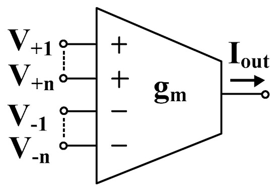
Figure 1.
Electrical symbol of MI-OTA.
The CMOS structure of the bulk-driven (BD) MI-OTA is shown in Figure 2a. It was first presented with a single current output in [30]. A simplified version of this OTA was also verified experimentally in [31,32]. Its input stage exploits a source degenerative linearization technique, first proposed for a gate-driven (GD) circuit operating in strong inversion; however, in a modified version proposed in [30], the gate-driven transistors were replaced by BD ones, that allows increasing both the linear and common-mode range of the circuit. Like in its GD counterpart, the transistors M1 and M2 form a differential pair, while transistors M15 and M16, operating in a triode region, introduce a negative feedback that leads to better linearity of the structure. The multiple inputs of the differential pair (MI-OTA) are realized by replacing the input transistors M1 and M2 with multiple-input BD devices, as shown in Figure 2b. The multiple inputs of these devices were realized using input capacitive dividers composed of the capacitors CB. Their values should be considerable larger than the parasitic capacitances of transistors M1 and M2. These CB capacitors could be realized on chip in any CMOS technology. In this work, the high reliability Metal-Insulator-Metal capacitors (MIM) offered by TSMC were used.
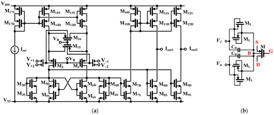
Figure 2.
CMOS implementation of proposed MI-OTA: (a) schematic, and (b) bulk-driven MI-MOST technique.
In order to properly bias the bulk terminals of the input devices for DC, the anti-parallel connections of the minimum-size transistors ML, operating in a cut-off region, with VGS = 0, were used.
The optimum linearity of the structure is obtained for m = (W/L)15,16/(W/L)1,2 = 0.5 [30]. The rest of the structure can be considered as current mirror OTA, with current mirrors M3S,D-M12S,D. In order to realize a second current output of the structure, required in the considered application, the composite self-cascode transistors M8S,D and M11S,D were doubled by M9S,D and M12S,D, respectively. In a single-output version, the additional transistors should be removed. Due to the fact that the voltage gain of the overall structure was lowered by the application of bulk-driven transistors with lower transconductance, and an input capacitive divider, MOS transistors in current mirrors were replaced by composite self-cascode transistors MiD-MiS, i = 3–14. This allows increasing of the output resistance, and consequently the DC voltage gain, without sacrificing the output voltage swing of the OTA. In addition, in order to further increase the overall voltage gain, a partial positive feedback was applied at the load of the first stage. The partial positive feedback is formed by the cross-coupled transistors M5S,D-M6SD, which create negative conductances, applied to the drain terminals of the diode-connected self-cascode transistors M3S,D and M4S,D, respectively. This lowers the resulting conductances at the drain terminals of M3S,D and M4S,D, thus increasing the current gain of the current mirrors M3S,D-M8S,D and M4S,D-M8S,D, and consequently the transconductance and voltage gain of the OTA. Note that in order to maintain the circuit stability in any circumstances, including process, voltage and temperature variations, as well as transistor mismatch, the transconductances of the transistors M5S,D-M6SD should always be lower than the transconductances of M3S,D and M4S,D. Additionally, since the circuit sensitivity increases as the difference of transconductances gm3,4SD-gm5,6SD decreases, this difference should not be too small, to maintain both the circuit sensitivity to mismatch, as well as the voltage excursion at the drains of M3,4SD, at an acceptable level. Thus, the relationship between transconductances of gm5,6SD and gm3,4SD is a result of a tradeoff between the circuit sensitivity to transistor mismatch, linear range and voltage gain. In the considered design it was assumed gm5,6SD = 0.3gm3,4SD, which increases the overall voltage gain by around 3 dB. Assuming unity gain current mirrors, and neglecting second-order effects, the OTA transconductance, determined from one differential input, can be expressed as follows:
where np is the subthreshold slope factor for a p-channel MOS, UT is the thermal potential, η = (1 − np) = gmb/gm is the ratio of the bulk to gate transconductances of a p-channel MOS at the operating point, and the attenuation factor β, represents the signal attenuation from the input capacitive divider. Assuming that the parasitic capacitances of the MOS transistors are small in comparison with CB, and for the frequency of the signal the impedances of capacitors CB are much smaller than the impedances of the biasing transistors ML, the coefficient β can be expressed as:
The coefficient BF in (2) represents the transconductance boosting factor coming from the partial positive feedback discussed above, which, neglecting the impact of output resistances of MOS transistors, can be approximated as:
where gmiSD represents a transconductance of a self-cascode composite transistor MiS-MiD. Note that in a weak inversion region, the transconductances are proportional to the biasing current flowing through corresponding devices. As can be concluded from (2), the overall transconductance is proportional to the biasing current Iset, and can easily be regulated using this current.
The low-frequency voltage gain of the OTA can be expressed by:
Thanks to all the techniques discussed above, the value of this gain can exceed 30 dB, despite the low voltage supply 0.5 V, lower transconductance of MOS transistors, and signal attenuation introduced by the input capacitive divider. Further, it is worth noting here that input noise of the MI-OTA will be increased due to the lower bulk transconductance, being a result of an input capacitive divider combined with a BD technique. However, the input range is extended in the same proportion, and hence, the dynamic range will not be affected and will be the same as for the gate-driven counterpart of the proposed OTA [30].
2.2. Proposed Shadow Oscillator
Figure 3 shows the block diagram of the shadow oscillator [3]. The system consists of a three-input single-output biquad filter and three amplifiers, A1, A2, and A3. Assume that the output Vo of the biquad filter can be expressed by:
where ε, β, α are real numbers of numerator and a, b are real numbers of a denominator which depends on the filter structure. The high-pass filter can be obtained if β = α = 0, the band-pass filter can be obtained if ε = α = 0, and the low-pass filter can be obtained if ε = β = 0.
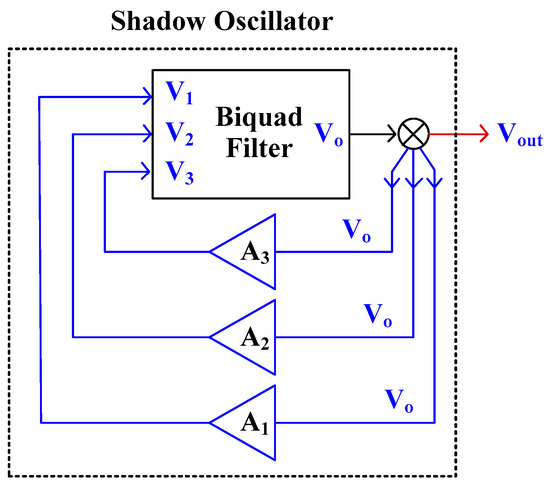
Figure 3.
Block diagram of shadow filter.
Considering the amplifiers, the outputs V1, V2, V3 of the amplifiers A1, A2, A3 can be expressed respectively by:
If voltages V1, V2, V3 are connected to the inputs of a biquad filter, the characteristic equation of the shadow oscillator can be expressed by:
The condition and the frequency of oscillation can be expressed, respectively, by:
Thus, the condition and the frequency of oscillation can be controlled independently by A2 and A3, respectively. The amplifier A1 can also be used to control the frequency of oscillation. However, the amplifier A1 is not significant and it can be removed for obtaining a minimum number of devices because amplifier A3 is already used to control the frequency of oscillation and it is enough to behave as a shadow oscillator. Thus, the multiple-input biquad filter that provides only low-pass and band-pass filters can be used.
Figure 4 shows the proposed shadow filters using MI-OTAs. Figure 4a shows the proposed shadow oscillator employing two single-output MI-OTAs, one dual-output MI-OTA, two grounded capacitors, and two grounded resistors. The gm1, gm2, C1, and C2 are used to realize the biquad filter. Using (1) and nodal analysis, the output Vo of the biquad filter can be given by:
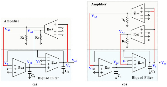
Figure 4.
Proposed shadow oscillator using MI-OTA for (a) obtaining minimum number of MI-OTAs, and (b) obtaining electronic tuning capability.
It should be noted that if V1 = Vin and V2 = 0 (connected to ground) the low-pass filter can be obtained; if V2 = Vin and V1 = 0 (connected to ground) the band-pass filter can be obtained.
The gm3, R1, and R2 are used to realize the amplifiers; the transfer function of the amplifiers can be expressed by:
Combining (11)–(13), the characteristic equation of the oscillator can be expressed by:
The condition and the frequency of oscillation can be given respectively by:
The condition of oscillation can be controlled by A2 through adjusting R2, and the frequency of oscillation can be controlled by A1 through adjusting R1 with constant gm3. Thus, the condition and the frequency of oscillation of the proposed shadow oscillator in Figure 4a can be independently controlled.
The shadow oscillator in Figure 4a is proposed for obtaining the minimum number of active elements, but the frequency of oscillation can be controlled by amplifier A1 through adjusting R1. Figure 4b shows the proposed shadow oscillator for obtaining an electronic tuning capability. It can be obtained by slightly modifying Figure 4a by adding an additional gm4. Thus, four single-output MI-OTAs are required. Using (1) and nodal analysis, the characteristic equation of the proposed oscillator in Figure 4b can be expressed by:
The condition and the frequency of oscillation can be given respectively by:
The condition of oscillation can be controlled electronically by A2 through adjusting gm3 and the frequency of oscillation can be controlled electronically by A1 through adjusting gm4. Thus, the condition and the frequency of oscillation of the proposed shadow oscillator in Figure 4b can be independently and electronically controlled.
The range for tuning the frequency of oscillation in (19) in terms of 1 + gm4R1 may be limited because this term is in a square-rooting form. Due to the gm4 providing multiple-input terminals, if the additional non-inverting terminal of gm4 is connected to Vo (red dashed line in Figure 4b), the term 1 + gm4R1 of (19) will become 1 + 2gm4R1. The range for tuning the frequency of the oscillator in this case will be increased compared with (19).
Considering the nodes Vo1 and Vo2 of the proposed shadow oscillators, the relationship of Vo1 and Vo2 is given by:
where gm3R1 ≈ 1 (or gm4R1 ≈ 1 for Figure 4b). It can be expressed that the phase difference of signals Vo1 and Vo2 are 90 (π/2) degree and the magnitude is |gm1/C1|. It should be noted that the magnitude of Vo1 and Vo2 will be constant if the values of gm1 and C1 are not used for varying the frequency of oscillation, like in conventional quadrature oscillators [14,18,19,20].
As is well-known, sinusoidal oscillators require an amplitude stabilization mechanism, which can exploit circuit nonlinearities, limiting large-signal loop gain for larger amplitudes, or a special automatic gain control (AGC) circuit [14,18,21]. In the proposed solution, the amplitude stabilization mechanism is based on circuit nonlinearities, which provides sufficient quality for the generated waveforms, while it does not require an additional, relatively complex, circuitry to realize the AGC loop. Note that, thanks to the shadow principle, the frequency of oscillations and the condition of oscillations can be controlled independently, which makes such a simple solution possible (frequency tuning does not affect the nonlinear mechanism limiting the frequency of oscillations, resulting in their constant amplitude). Note that similar solutions, based on exploiting the circuit nonlinearities, were applied in some other shadow oscillators available in literature, such as [22,23]. However, in more demanding cases, a special AGC circuit could also be applied in the proposed oscillator. In the version described in this work, the amplitude of oscillations is approximately equal to the linear range of the used OTAs.
The effect of OTA parasitic elements on the performance of the shadow oscillator is considered using the equivalent circuit that represents a non-ideal OTA with finite parasitic resistances and capacitances in [41]. These finite parasitic resistance and capacitances will appear if the OTA operates near the cut-off frequency. As the input terminal of the proposed OTA in Figure 2 is connected to the parallel floating of high-resistance ML and floating capacitance CB, the parasitic resistance and capacitance at the input terminal will be neglected. Thus, only parasitic resistance and capacitance at the output terminal Ro and Co will be considered. Letting Co1//Ro1, Co2//Ro2, and Co3//Ro3 are the parasitic parameters of OTA1, OTA2, and OTA3, respectively. Consider Figure 4a: external capacitors C1 and C2 are parallel connected at the node Vo1 and Vo2, thus the effects of parasitic capacitances Co1 and Co2 can be neglected if C1 >> Co1 and C2 >> Co2, while the effects of parasitic resistors Ro1 and Ro2 can be reduced if the operating frequency of the circuit is ωo >> max[1/(C1 + Co1)Ro1, 1/(C2 + Co2)Ro2)] [42]. The voltage gains A1 and A2 in (12) and (13) become gm3(R1//Ro3) and gm3(R2//Ro3), respectively. This parasitic resistance Ro3 can be absorbed if R1 << Ro3 and R2<<Ro3 while the parasitic impedances at nodes VA1 and VA2 are (Ro3//Co3), respectively. The effects of parasitic impedances at nodes VA1 and VA2 will be alleviated if the frequency of operation is smaller than 1/(Ro3//Co3). However, since the circuit operates at very low frequencies, the impact of parasitic elements on the circuit operation is expected to be low.
3. Simulation Results
The CMOS structure of the MI-OTA and the shadow oscillator were designed and simulated in Cadence program using 0.18 µm CMOS technology from TSMC. The transistor aspect ratio is shown in Table 1. The MIM input capacitors CB = 0.5 pF. The voltage supply is 0.5 V for nominal value of Iset = 10 nA, and the power consumption of the two- and one-output OTA is 15.25 nW and 13.5 nW, respectively. The basic parameters of the MI-OTA can be found in [30] as follows: the DC voltage gain is 31.17 dB, common mode rejection ratio is 90.05, power supply rejection ratio is 37.26 dB and input offset is 0.224 mV with 20 pF load capacitance.

Table 1.
Transistor aspect ratio of the MI-OTA.
Figure 5 shows the output current and the transconductance of the MI-OTA versus the input voltage and various Iset = 10 nA, 20 nA and 30 nA. The high linearity with wide input voltage range of ± 230 mV is notable. For instance, for this input voltage range and for Iset = 10 nA (gm = 26.4 nS), the deviation of the transconductance value is below 5%. The high linearity under 0.5V supply voltage is obtained thanks to the bulk-driven multiple-input technique and the negative feedback.
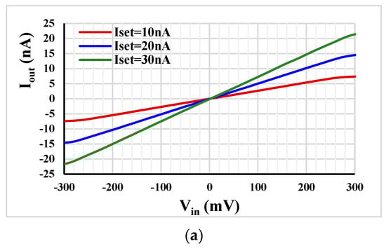
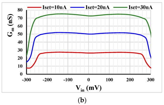
Figure 5.
The MI-OTA output current (a) and the transconductance (b) versus the input voltage with various Iset.
The shadow oscillator was simulated with nominal Iset = Iset1,2,3,4 = 10 nA, the off-chip passive elements C1 = C2 = 20 pF. The nominal power consumptions of the shadow oscillators in Figure 4 (a) and (b) were 42.25 nW and 54 nW, respectively. From (15) and (16), it can be concluded that the condition of oscillation can be controlled by gm3R2 (A2) and the frequency of oscillation can be given by gm3R1 (A1), thus R2 = 42 MΩ was selected to satisfy (15) (gm3 = 26.4 nS) and R1 = 100 kΩ was given the oscillating frequency in (16), whereas the core parameters of oscillator, gm1 = gm2 = 26.4 nS and C1 = C2 = 20 pF are constant. Figure 6a,b shows the running oscillation and steady state, respectively. The outputs Vo1 and Vo2 are in quadrature with frequency of 202 Hz. This result confirms that the condition of oscillation can be controlled by amplifier A2 (gm3R2).
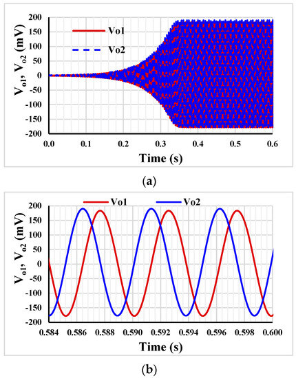
Figure 6.
The running oscillation (a) and the steady state (b).
The Fast Fourier Transform (FFT) of Vo1 and Vo2 is shown in Figure 7. The Total Harmonic Distortions (THDs) for Vo1 and Vo2 were 0.397% and 0.35%, respectively.
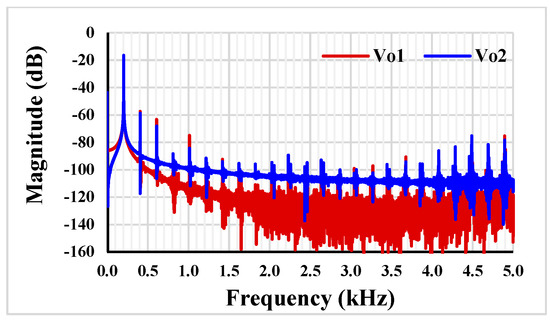
Figure 7.
The FFT for Vo1 and Vo2.
Figure 8 shows the relation between Vo1 and Vo2 that can confirm the quadrature relationship of output signals. It can be noticed that the amplitudes of Vo1 and Vo2 are nearly equal at frequency of 202 Hz.
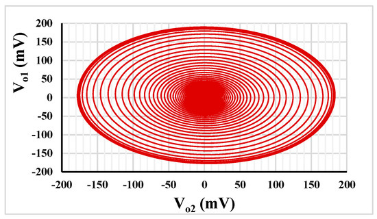
Figure 8.
The quadrature relationship between Vo1 and Vo2.
Table 2 shows the impact of the temperature and process corners on the performance of the oscillator. The temperature corners were −20 °C, 27 °C and 50 °C; the process corners were fast-fast (FF), fast-slow (FS), slow-fast (SF) and slow-slow (SS). The oscillator is capable of oscillating under all temperature and process conditions thanks to the tuning capability of the condition and frequency of oscillation. The required frequency can be simply readjusted by the setting currents.
Table 2.
Temperature and process corners analysis.
Figure 9a shows the frequency tuning capability of the oscillator in Figure 4a with Iset1,2,3 = 10 nA versus R1 = 0.1 MΩ, 1 MΩ and 5 MΩ. Figure 9b shows the extra freedom of electronic tunability that was offered by the oscillator in Figure 4b with Iset1,2,3 = 10 nA and various Iset4 = 10 nA, 20 nA, 30 nA. This result confirms that the frequency of the oscillator can be controlled by the amplifier A1 (gm3R1 and gm4R1).
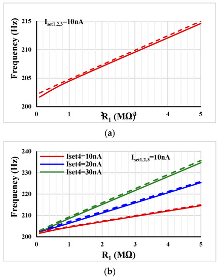
Note that the electronically adjustable gm via Iset is used in this design for fine-tuning of the oscillator frequency; hence, it enables readjusting of the required frequency in case of its deviation after fabrication. If wider tuning range is needed then the Iset should be increased, at the cost of increased power consumption of the application.
The amplitudes of Vo1 and Vo2 versus the oscillation frequencies from Figure 4a,b are shown in Figure 10a,b, respectively. It can be noticed that, thanks to the shadow principle, the amplitude of output signals is only slightly changed when the oscillation frequencies are varied by amplifiers.
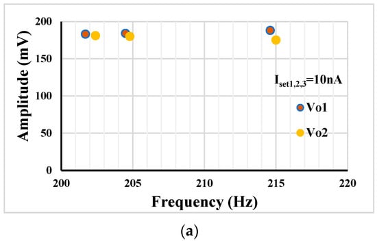
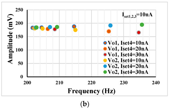
Figure 10.
The amplitudes of Vo1 and Vo2 versus the oscillation frequencies (a) varying by R1, and (b) varying by gm4 via Iset4.
Figure 11 shows the amplitude versus oscillation frequency in case of tuning Iset1,2 = 10 nA, 20 nA and 25 nA. Here, due to the lack of the shadow principle, the decreasing amplitude with increase of the frequency is notable. Comparing Figure 11 with Figure 10, it can be concluded that the shadow oscillator that tunes the frequency by an amplifier offers less amplitude change of the output signal.
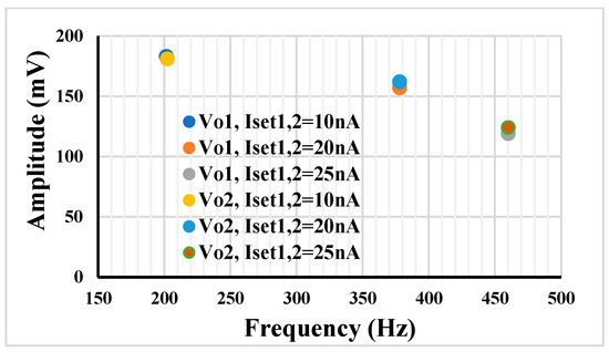
Figure 11.
The amplitudes of Vo1 and Vo2 versus the oscillation frequencies when Iset1 and Iset2 are varied.
Figure 12a shows the results of Monte Carlo (MC) process and mismatch analysis, with 200 runs, for Vo1 (a) and Vo2 (b). The mean frequency value was 195 Hz and the standard deviation was 15.27 Hz.
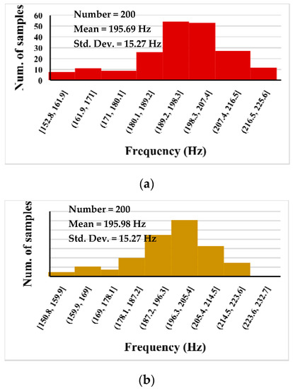
Figure 12.
200-run MC analysis for Vo1 (a) and Vo2 (b).
The proposed shadow oscillators have been compared in Table 3 with previous works [14,21,22,23]. Both types of oscillators with amplitude stabilization based on AGC circuits [14,21], as well as circuit nonlinearities [22,23], have been selected for comparison. The proposed oscillator using an amplifier to vary the frequency has a simpler structure compared with [14,21] that use AGC circuits to control the amplitude. Compared to [22], the proposed oscillator enjoys an electronic control, and compared to [23], the proposed oscillator enjoys independent control. Compared to all previous works [14,21,22,23], the proposed structure consumes ultra-low levels of power, rendering it suitable for extremely low-voltage and low-power applications such as biomedical systems.
Table 3.
Comparison of the proposed shadow oscillators with previous works.
4. Conclusions
This paper presents a low-voltage and nano-power shadow oscillator based on MI-OTA for low-frequency applications. The proposed oscillator uses two-input single-output biquad filter and amplifiers. The condition and the frequency of oscillation of the shadow oscillator can be controlled electronically and independently using amplifiers. The oscillator can be tuned by resistor, capacitor and by the setting current Iset. The simulated results show low THD (around 0.39%) for both output signals and acceptable tuning range. The 0.5 V supply voltage and the 54 nW power consumption of the oscillator is another benefit of the proposed circuit.
Author Contributions
Conceptualization, F.K., M.K. and T.K.; methodology, M.K., F.K. and M.Y.; software, M.K. and F.K.; validation, F.K. and T.K.; formal analysis, T.K., M.K. and F.K., investigation, F.K., M.Y. and M.K.; resources, F.K. and M.K.; writing—original draft preparation, F.K., T.K., M.Y. and M.K.; writing—review and editing, F.K. and T.K.; visualization, F.K., T.K. and M.K.; supervision, F.K.; project administration, F.K.; funding acquisition, F.K. All authors have read and agreed to the published version of the manuscript.
Funding
This work was supported by the University of Defence within the Organization Development Project VAROPS.
Institutional Review Board Statement
Not applicable.
Informed Consent Statement
Not applicable.
Data Availability Statement
Not applicable.
Conflicts of Interest
The authors declare no conflict of interest.
References
- Lakys, Y.; Fabre, A. Shadow filters: New family of second-order filters. Electron. Lett. 2010, 46, 276–277. [Google Scholar] [CrossRef]
- Biolkova, V.; Biolek, D. Shadow filters for orthogonal modification of characteristic frequency and bandwidth. Electron. Lett. 2010, 46, 830–831. [Google Scholar] [CrossRef]
- Abuelma’Atti, M.T.; Almutairi, N.R. New current-feedack operational-amplifier based shadow filters. Analog. Integr. Circuits Signal Process. 2016, 86, 471–480. [Google Scholar] [CrossRef]
- Alaybeyoğlu, E.; Kuntman, H. A new frequency agile filter structure employing CDTA for positioning systems and secure communications. Analog. Integr. Circuits Signal Process. 2016, 89, 693–703. [Google Scholar] [CrossRef]
- Singh, D.; Paul, S.K. Realization of current mode universal shadow filter. AEU Int. J. Electron. Commun. 2020, 117, 153088. [Google Scholar] [CrossRef]
- Nand, D.; Pandey, N. New Configuration for OFCC-Based CM SIMO Filter and its Application as Shadow Filter. Arab. J. Sci. Eng. 2018, 43, 3011–3022. [Google Scholar] [CrossRef]
- Khateb, F.; Jaikla, W.; Kulej, T.; Kumngern, M.; Kubánek, D. Shadow filters based on DDCC. IET Circuits Devices Syst. 2017, 11, 631–637. [Google Scholar] [CrossRef]
- Huaihongthong, P.; Chaichana, A.; Suwanjan, P.; Siripongdee, S.; Sunthonkanokpong, W.; Supavarasuwat, P.; Jaikla, W.; Khateb, F. Single-input multiple-output voltage-mode shadow filter based on VDDDAs. AEU Int. J. Electron. Commun. 2019, 103, 13–23. [Google Scholar] [CrossRef]
- Buakaew, S.; Narksarp, W.; Wongtaychatham, C. Shadow bandpass filter with Q-improvement. In Proceedings of the 2019 5th International Conference on Engineering, Applied Sciences and Technology (ICEAST), Luang Prabang, Laos, 2–5 July 2019; pp. 1–4. [Google Scholar] [CrossRef]
- Buakaew, S.; Narksarp, W.; Wongtaychatham, C. High quality-factor shadow bandpass filters with orthogonality to the characteristic frequency. In Proceedings of the 2020 17th International Conference on Electrical Engineering/Electronics, Computer, Telecommunications and Infor-mation Technology (ECTI-CON), Phuket, Thailand, 24–27 June 2020; pp. 372–375. [Google Scholar] [CrossRef]
- Buakaew, S.; Wongtaychatham, C. Boosting the quality factor of the shadow bandpass filter. J. Circuits Syst. Comput. 2022, 31, 2250248. [Google Scholar] [CrossRef]
- Lathi, B.P. Modern Digital and Analog Communication Systems; Oxford University Press: New York, NY, USA, 1998. [Google Scholar]
- Dobkin, B.; Williams, J. Analog Circuit Design; Elsevier: Amsterdam, The Netherlands, 2013. [Google Scholar]
- Jaikla, W.; Adhan, S.; Suwanjan, P.; Kumngern, M. Current/Voltage Controlled Quadrature Sinusoidal Oscillators for Phase Sensitive Detection Using Commercially Available IC. Sensors 2020, 20, 1319. [Google Scholar] [CrossRef]
- Horng, J.-W. A sinusoidal oscillator using current-controlled current-conveyors. Int. J. Electron. 2001, 88, 659–664. [Google Scholar] [CrossRef]
- Bhaskar, D.R.; Senani, R.; Singh, A.K. Linear sinusoidal VCOs: Newconfigurations using current feedback op-amps. Int. J. Electron. 2010, 97, 263–272. [Google Scholar] [CrossRef]
- Biolek, D.; Lahiri, A.; Jaikla, W.; Siripruchyanun, M.; Bajer, J. Realization of electronically tunable voltage-mode/current-mode quadrature sinusoidal oscillator using ZC-CG-CDBA. Microelectron. J. 2011, 42, 1116–1123. [Google Scholar] [CrossRef]
- Borah, S.S.; Singh, A.; Ghosh, M.; Ranjan, A. Electronically tunable higher-order quadrature oscillator employing CDBA. Microelectron.J. 2021, 108, 104985. [Google Scholar] [CrossRef]
- Herencsar, N.; Lahiri, A.; Vrba, K.; Koton, J. An electronically tunable current-mode quadrature oscillator using PCAs. Int. J. Electron. 2012, 99, 609–621. [Google Scholar] [CrossRef]
- Sotner, R.; Hrubos, Z.; Herencsar, N.; Jerabek, J.; Dostal, T.; Vrba, K.; Sotner, R.; Hrubos, Z.; Herencsar, N.; Jerabek, J.; et al. Precise electronically adjustable oscillator suitable for quadrature signal generation employing active elements with current and voltage gain control. Circuits, Syst. Signal Process. 2013, 33, 1–35. [Google Scholar] [CrossRef]
- Herencsar, N.; Minaei, S.; Koton, J.; Yuce, E.; Vrba, K. New resistorless and electronically tunable realization of dual-output VM all-pass filter using VDIBA. Analog. Integr. Circuits Signal Process. 2012, 74, 141–154. [Google Scholar] [CrossRef]
- Abuelma’Atti, M.T.; Almutairi, N. A novel shadow sinusoidal oscillator. Int. J. Electron. Lett. 2016, 5, 291–302. [Google Scholar] [CrossRef]
- Buakaew, S.; Atiwongsangthong, N. Adjustable quadrature shadow sinusoidal oscillator. In Proceedings of the 2022 8th International Conference on Engineering, Applied Sciences, and Technology (ICEAST), Chiang Mai, Thailand, , 8–10 June 2022; pp. 42–45. [Google Scholar] [CrossRef]
- Rubio, F.J.; Dominguez, M.A.; Perez-Aloe, R.; Carrillo, J.M. Current-mode electronically-tunable sinusoidal oscillator based on a shadow bandpass filter. In Proceedings of the 2022 18th International Conference on Synthesis, Modeling, Analysis and Simulation Methods and Applications to Circuit Design (SMACD), Villasimius, Italy, 12–15 June 2022; pp. 1–4. [Google Scholar] [CrossRef]
- Veeravalli, A.; Sanchez-Sinencio, E.; Silva-Martinez, J. A CMOS Transconductance Amplifier Architecture with Wide Tuning Range for Very Low Frequency Applications. IEEE J. Solid-State Circuits 2002, 37, 776–781. [Google Scholar] [CrossRef]
- Wang, M.; Saavedra, C.E. Very low frequency tunable signal generator for neural and cardiac cell stimulation. Int. J. Electron. 2011, 98, 1215–1227. [Google Scholar] [CrossRef]
- Miyazaki, T.; Lim, S.T.; Minamitake, C.; Takeishi, T. Ultralow-frequency oscillator with switched capacitors. Electron. Commun. Jpn. 1992, 75, 98–106. [Google Scholar] [CrossRef]
- Elwakil, A.S. Systematic realization of low-frequency oscillators using composite passive–active resistors. IEEE Trans. Instrum. Meas. 1998, 47, 584–586. [Google Scholar] [CrossRef]
- Senani, R.; Bhaskar, D. Single Op-Amp Sinusoidal Oscillators Suitable for Generation of Very Low Frequencies. IEEE Trans. Instrum. Meas. 1991, 40, 777–779. [Google Scholar] [CrossRef]
- Khateb, F.; Kulej, T.; Akbari, M.; Kumngern, M. 0.5-V High Linear and Wide Tunable OTA for Biomedical Applications. IEEE Access 2021, 9, 103784–103794. [Google Scholar] [CrossRef]
- Khateb, F.; Kulej, T.; Kumngern, M.; Psychalinos, C. Multiple-input bulk-driven MOS transistor for low-voltage low-frequency applications. Circuits Syst. Signal Process. 2018, 38, 2829–2845. [Google Scholar] [CrossRef]
- Khateb, F.; Kulej, T.; Akbari, M.; Tang, K.-T. A 0.5-V multiple-input bulk-driven OTA in 0.18-μm CMOS. IEEE Trans. Very Large Scale Integr. (VLSI) Syst. 2022, 30, 1739–1747. [Google Scholar] [CrossRef]
- Parvizi, M. Design of a new low power MISO multi-mode universal biquad OTA–C filter. Int. J. Electron. 2018, 106, 440–454. [Google Scholar] [CrossRef]
- Aggarwal, B.; Gupta, A. QFGMOS and FGMOS based low-voltage high performance MI-OTA. Int. J. Inf. Technol. 2020, 13, 415–422. [Google Scholar] [CrossRef]
- Khateb, F.; Prommee, P.; Kulej, T. MIOTA-based Filters for Noise and Motion Artifact Reductions in Biosignal Acquisition. IEEE Access 2022, 10, 14325–14338. [Google Scholar] [CrossRef]
- Kumngern, M.; Aupithak, N.; Khateb, F.; Kulej, T. 0.5V Fifth-Order Butterworth Low-Pass Filter Using Multiple-Input OTA for ECG Applications. Sensors 2020, 20, 7343. [Google Scholar] [CrossRef]
- Prommee, P.; Karawanich, K.; Khateb, F.; Kulej, T. Voltage-Mode Elliptic Band-Pass Filter Based on Multiple-Input Transconductor. IEEE Access 2021, 9, 32582–32590. [Google Scholar] [CrossRef]
- Veeravalli, A.; Sánchez-Sinencio, E.; Silva-Martínez, J. Transconductance amplifier structures with very small transconductances: A comparative design approach. IEEE J. Solid-State Circuits 2002, 37, 770–775. [Google Scholar] [CrossRef]
- Colletta, G.D.; Ferreira, L.H.C.; Pimenta, T.C. A 0.25-V 22-nS symmetrical bulk-driven OTA for low frequency Gm-C applications in 130-nm digital CMOS process. Analog. Integr. Circuits Signal Process. 2014, 81, 377–383. [Google Scholar] [CrossRef]
- Cotrim, E.D.; Ferreira, L.H.C. An ultra-low-power CMOS symmetrical OTA for low-frequency Gm-C applications. Analog Integr. Circ. Signal Process 2012, 71, 275–282. [Google Scholar]
- Wang, S.-F.; Chen, H.-P.; Ku, Y.; Lee, C.-L. Versatile Voltage-Mode Biquadratic Filter and Quadrature Oscillator Using Four OTAs and Two Grounded Capacitors. Electronics 2020, 9, 1493. [Google Scholar] [CrossRef]
- Wang, S.-F.; Chen, H.-P.; Ku, Y.; Lin, Y.-C. Versatile Tunable Voltage-Mode Biquadratic Filter and Its Application in Quadrature Oscillator. Sensors 2019, 19, 2349. [Google Scholar] [CrossRef]
Disclaimer/Publisher’s Note: The statements, opinions and data contained in all publications are solely those of the individual author(s) and contributor(s) and not of MDPI and/or the editor(s). MDPI and/or the editor(s) disclaim responsibility for any injury to people or property resulting from any ideas, methods, instructions or products referred to in the content. |
© 2023 by the authors. Licensee MDPI, Basel, Switzerland. This article is an open access article distributed under the terms and conditions of the Creative Commons Attribution (CC BY) license (https://creativecommons.org/licenses/by/4.0/).