1. Introduction
Among the various functions of CMOS image sensors (CISs), time-of-flight (ToF) range image sensors are receiving much attention for new markets and applications of CISs, including consumer, industrial, and scientific applications [
1,
2,
3]. ToF range sensor applications require high precision, accuracy, linearity, and tolerance to ambient light. Direct-type ToF imagers using a single-photon avalanche diode, and all-digital-domain processing are excellent for high-accuracy ToF [
4,
5,
6,
7]. However, it requires complex hardware, specifically, if there is a need for extremely high-resolution and tolerance to ambient light. Indirect-type ToF imagers have an advantage of small pixel size, less circuit complexity, and relatively reliable range resolution, specifically for range measurements of a few meters. Two types of indirect ToF imaging methods exist, depending on the waveform of the modulated light. One is continuous wave (CW)-based [
8,
9,
10,
11,
12,
13,
14,
15], and the other is short pulse (SP)-based [
16,
17,
18,
19,
20,
21,
22,
23,
24]. The SP-based indirect ToF has a better tolerance to ambient light because the light power is concentrated on the short pulse, and the charge-draining function of the ToF pixel reduces the influence of the ambient light. However, because of the analog-domain processing for ToF measurement, the SP-based indirect ToF sensor suffers from various analog imperfections, such as the nonlinearity of the pixel source-follower amplifier, the distortion of the waveform of the light pulse, finite photo-carrier response time in the photodiode, and the distortion of the gating pulse for demodulation. The full-well capacity of the pixel limits the range resolution or depth noise of indirect ToF sensors if the photon-shot noise is the liming factor of the range resolution [
3]. Using a short pulse is effective for improving the range resolution. High-resolution ToF sensors designed with a pixel using a very short light pulse lower than 100 ps and a large full-well capacity larger than 1M electrons have range resolutions of sub-millimeter [
25] and sub-100 micrometer [
26]. Because of the short pulse, the nonlinearity and skew of the gating pulses become significant issues to be solved. Complicated off-line processing for nonlinearity correction and the on-chip skew calibration circuits are necessary for implementing a linear array ToF sensor.
To address to the issues of the SP-based indirect ToF sensors, this paper proposes an SP-based indirect ToF image sensor using the time-domain negative feedback technique. To the best of our knowledge, this work is the first attempt at a indirect ToF image sensor using a time-domain negative feedback technique. In the conventional indirect ToF image sensors, open-loop analog interface circuits and a successive analog-to-digital converter (ADC) are used. Techniques for improving their linearity and range resolution, respectively, are based on the design effort of the open-loop analog readout circuits like source followers and having a high demodulation frequency (or short pulse width) and high-full-well capacity [
10,
26]. A negative feedback technique in analog circuits and systems is known as an effective way for improving the nonlinearity, frequency response, and stability [
27,
28]. In the proposed design, the negative feedback technique is used at the time-domain for coarse and fine ToF measurements. The negative feedback used for coarse ToF measurements is based on finding zero of the ToF difference from the delay of gating pulses generated by a digital-to-time converter (DTC), effectively improving the linearity by maintaining a constant operating point of analog readout circuits. In fine ToF measurements, a first-order delta-sigma modulation (DSM) loop using time-domain feedback is used. The DSM loop using one-bit analog-to-digital converter (ADC) and one-bit digital-to-analog converter, which is popular for audio ADCs, has a self-contained property of low distortion and noise using oversampling signal processing [
29,
30,
31]. It provides high-linearity and range resolution in ToF measurements if it is applied as the DSM using the time-domain feedback. A prototype chip for the concept proof is implemented, and the linearity and resolution are characterized.
The rest of the paper is organized into
Section 2 describing the principle of ToF measurements using time-domain feedback.
Section 3 describes the circuit design, and
Section 4 provides the results of the ToF measurement system implementation and measurements.
Section 5 presents the concluding remarks.
2. ToF Measurement Using Time-Domain Feedback
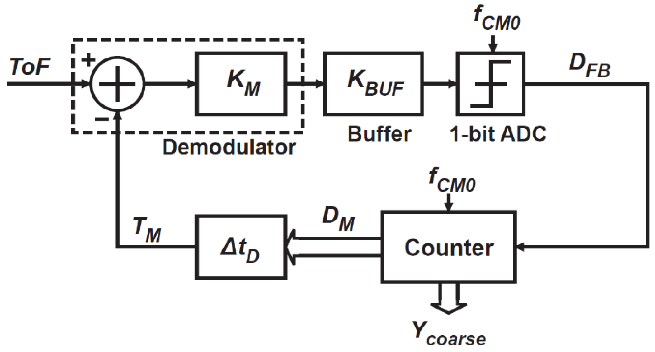
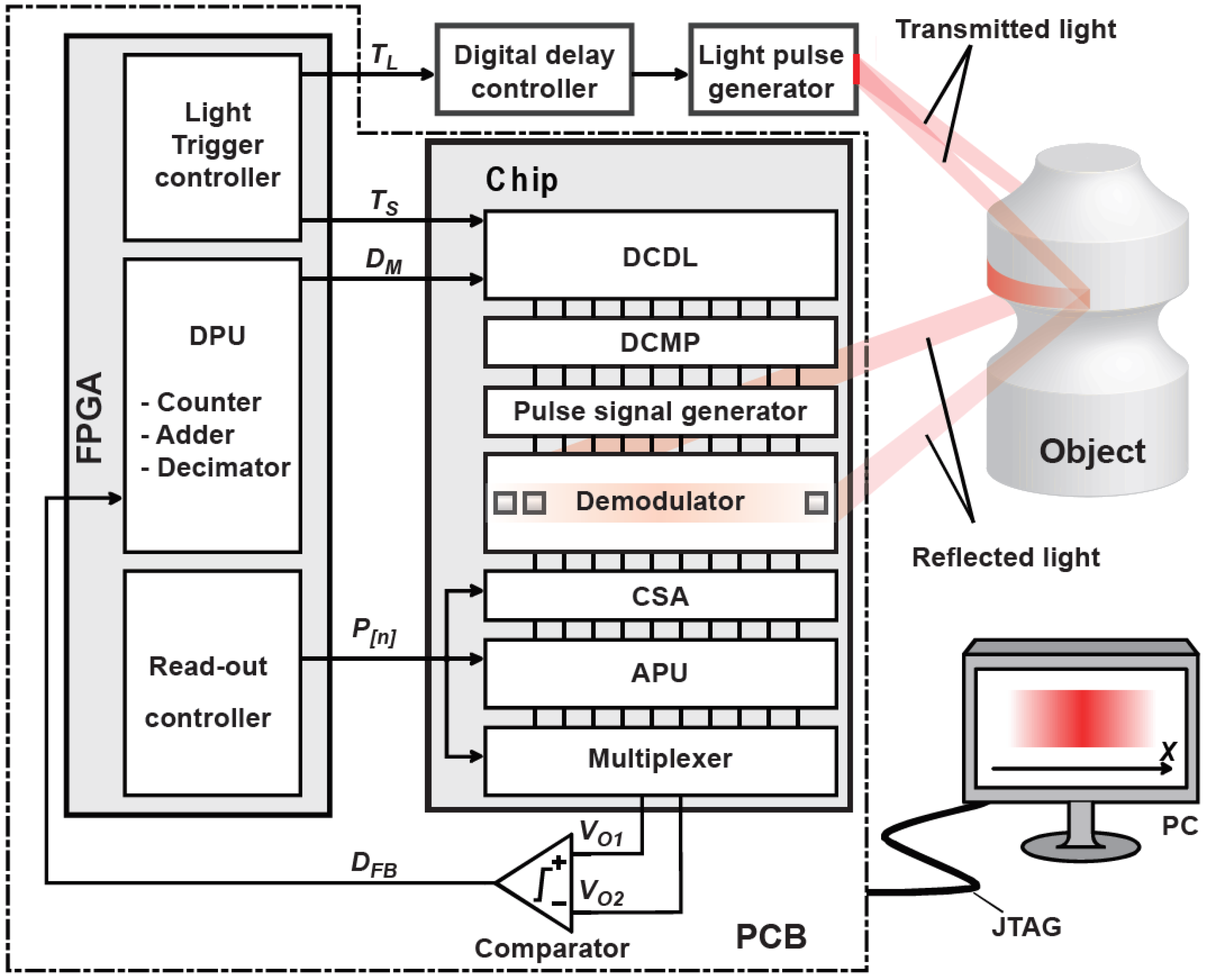
Figure 1 shows a system diagram of the proposed sensor. The light pulse emitted from the light source is reflected onto the object and converted into an electrical signal by a photodiode (PD) and a demodulator. The time-domain negative feedback loop consists of a demodulator, analog processing unit (APU), 1-bit ADC, digital processing unit (DPU), and digital-to-time converter (DTC). This system measures the ToF with high linearity and resolution. To cover the wide range of ToF measurements while maintaining high-linearity and range resolution, the system in
Figure 1 works with a coarse and fine measurement step. To realize the coarse and fine measurements with the time-domain negative feedback loop, each APU and DPU have two switchable functions. In the coarse measurement, a buffer amplifier and digital counter are used for the APU and DPU, respectively, working as an incremental ToF-to-digital conversion. In the fine measurement, an integrator and digital adder are used for the APU and DPU, respectively, working as a first-order DSM.
2.1. Incremental Time-to-Digital Conversion for Coarse ToF Measurements
Figure 2 shows an equivalent block diagram for coarse ToF measurements, consisting of a demodulator, buffer gain stage, 1-bit ADC, digital counter, and DTC. This system works as an incremental time-to-digital conversion (TDC). The demodulator senses the time position of ToF, and the demodulated charges are converted into a voltage signal at the buffer stage. With the time-domain feedback with DTC output, the voltage signal output of the demodulator with the buffer gain stage is expressed as
where
is the time-to-voltage conversion gain of the demodulator,
is the voltage gain of the buffer, and
is the DTC output in the time-domain. The 1-bit ADC quantizes the buffer output with a threshold of zero, and the increment code for the digital domain feedback,
, is generated as
The
is given to a counter where the number of 1’s is counted, and the counter output at the
n-th step,
, is expressed as
The delay of DTC output at the
n-th step,
, which is the time-domain feedback to the demodulator, is given by
where
is the conversion factor of DTC, which is equal to the DTC unit delay step.
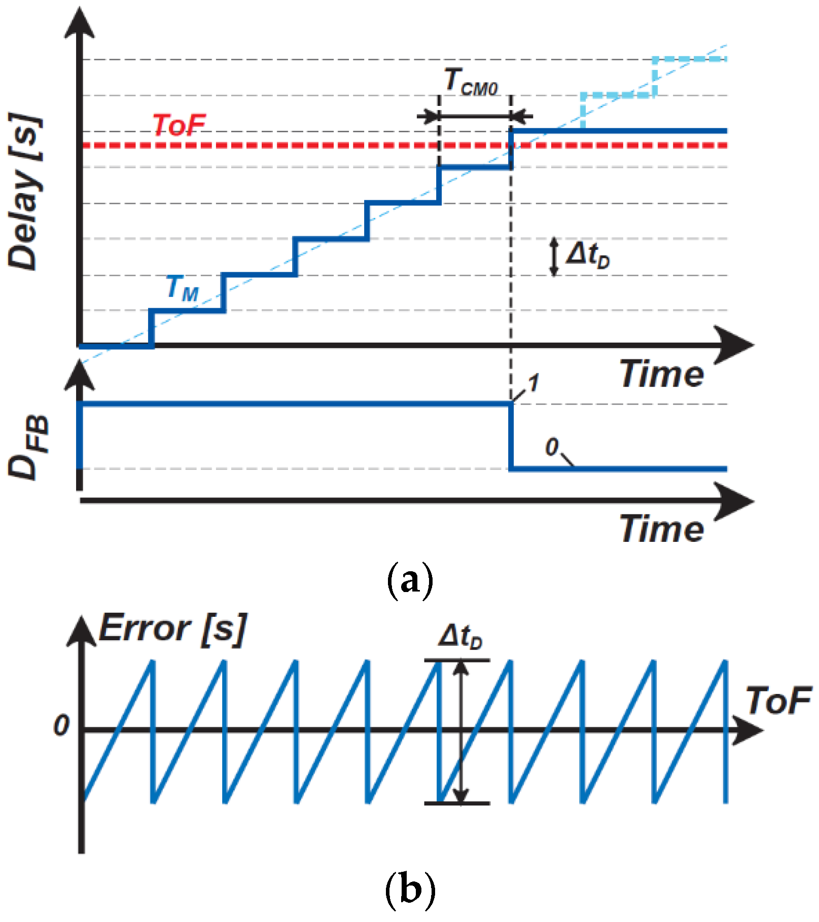
Figure 3 shows a simplified conceptual operating waveform and the ToF quantization error. To coarsely measure ToF using the incremental TDC, the initial value of the counter output,
, is set to zero so that
is initially set to zero and
is gradually approximated step-by-step to ToF, expressed as a set of the above equations. While
is 1, the DTC delay is incremented. When
becomes larger than ToF,
becomes 0 and the DTC output delay increment is stopped. When this happens at the
-th step, the counter output is expressed as
The counter output at the final step,
, is also
because the counter output is not incremented after the
-th step, where
is the maximum number of DTC delay steps. The DTC output at the final step,
, is given by
. The difference between the ToF and
is the error of the measured ToF because of the incremental TDC in the coarse ToF measurement mode. The error is maximal within the range of
to
(
Figure 3b). The maximum ToF measurement range is
, given by
The output of the coarse ToF measurements,
, is the final code stored in the counter as
The time required for doing the coarse ToF measurement time, , is expressed as if the time required for doing one step for the gradual approximation is .
2.2. DSM for Fine ToF Measurements
Figure 4 shows an equivalent block diagram for fine ToF measurements, employing a first-order delta-sigma modulation (DSM) with time-domain negative feedback. Though the use of higher-order DSMs has more efficient improvement of SNR to the oversampling ratio used, the first-order DSM is employed for an area-efficient column-wise implementation with a limited column pitch. In this fine ToF measurement mode, an integrator and adder are used for the APU and DPU, respectively. The adder adds coarse ToF measurement results stored in the counter, and the DSM finely measures the ToF difference from a coarse estimate of it,
. From
Figure 4, the DSM output
DFB[
z] is expressed as
where
is the gain of the integrator,
is the quantization noise of the 1-bit ADC, and
is the difference of
to the time domain feedback, expressed as
By substituting Equation (9) into (8), the overall system response in the z-domain for the DSM part of
Figure 4 is expressed as
where
is the gain of the integrator, and
is the quantization noise of the 1-bit ADC. The conventional first-order DSM using a 1-bit ADC shows that the loop gain of the modulator is unity if the modulator is stably operated [
31]. Therefore, the condition
is met, and the equation is simplified as
From Equation (11), transfer functions to signal and quantization noise are obtained. The signal transfer function, the relationship between
and
, is the same as the inverse of the DTC delay step. The noise transfer function (NTF), the relationship between
and
, is
. In order to estimate the quantization noise using the DSM, it is useful to find the squared magnitude of NTF in the frequency domain [
30] by setting
, given by
where
is the frequency,
is the period of the oversampling, and
is the oversampling frequency.
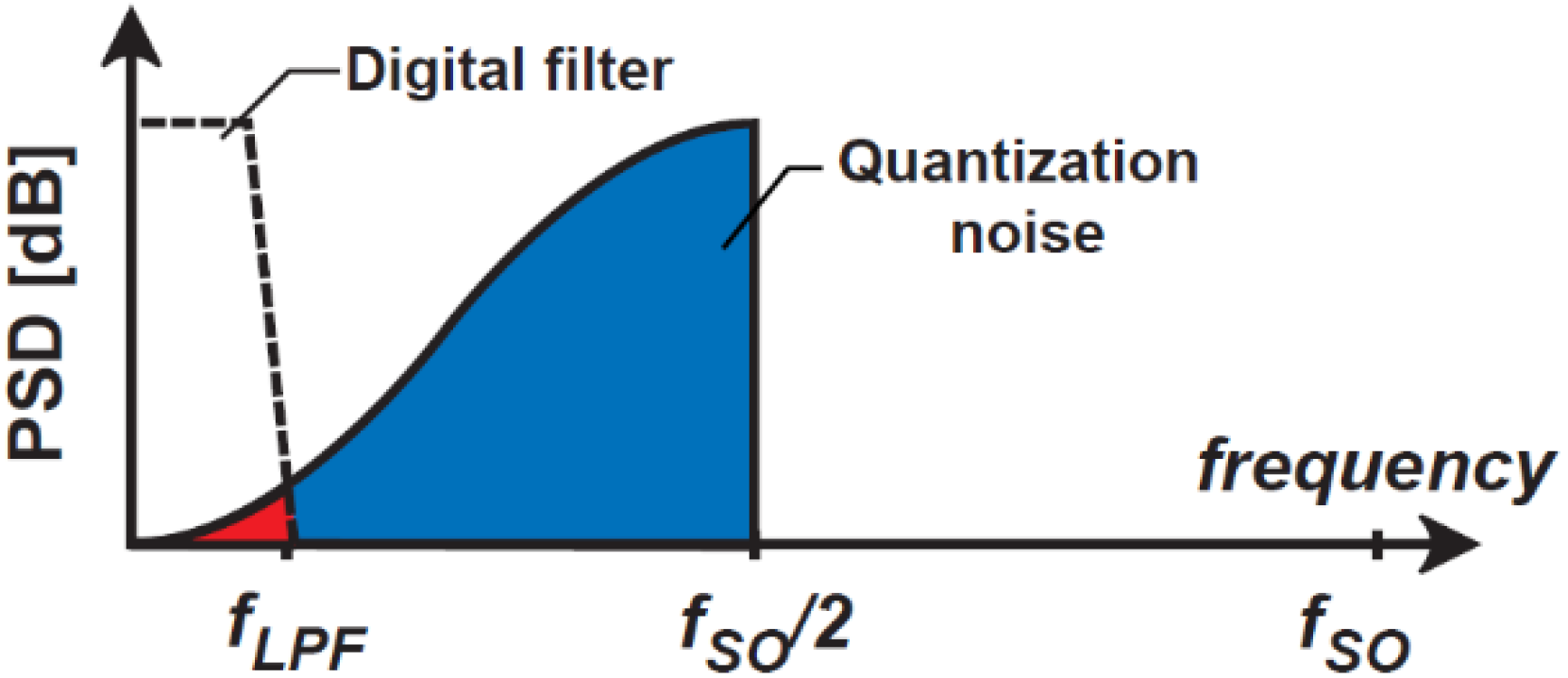
Figure 5 shows the power spectrum density (PSD) due to the shaped quantization noise through the NTF given by Equation (10). The shaped quantization noise is reduced using a digital low-pass filter (LPF) with a cutoff frequency of
. Then, the ratio of the square root of the residual noise power (the red colored area) to the entire quantization noise (the sum of the red and blue colored areas) gives the increase of the effective number of bits (ENOB) in the fine TDC. With the oversampling ratio denoted by
and given by
, the area ratio of red-colored to (red + blue)-colored is approximately
[
30,
31]. Then the ENOB increase using an ideal LPF denoted by
is given by
In this proposed technique using the first-order DSM,
[bit] is obtained for
of 4. However, this is the case that an ideal low-pass filter, which has very steep cutoff, is used. In the actual implementation, a very simple counter that counts the number of 1’s in the bit-stream is used for the low-pass filtering. Because the counter does not have steep cutoff and its frequency response is like a moving average filter, the residual quantization noise power after low-pass filtering is
of the entire quantization noise. The increase in the effective number of bits (denoted by
) in this case is given by
In the actual implementation, (or 66 for error reduction) and a counter-based low-pass filter is used, and the ENOB increase in the fine TDC implementation is 6 bits. From Equation (14), doubling the oversampling ratio can increase the ENOB by another one bit, while having the penalty of doubling the processing time of the fine ToF measurement. The filtered output of the DSM linearly responds to the , and a fine TDC for fine ToF measurement is realized.
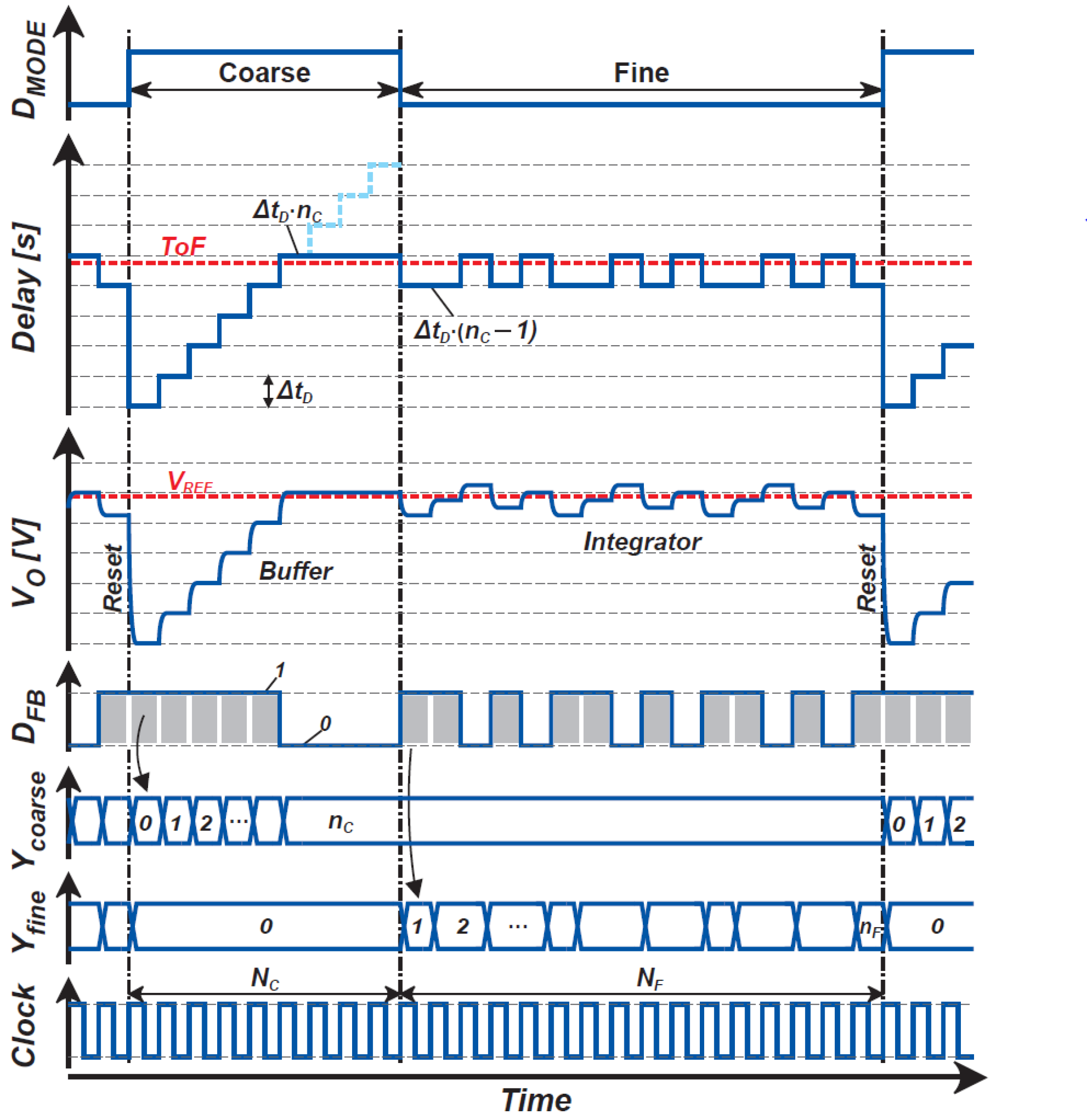
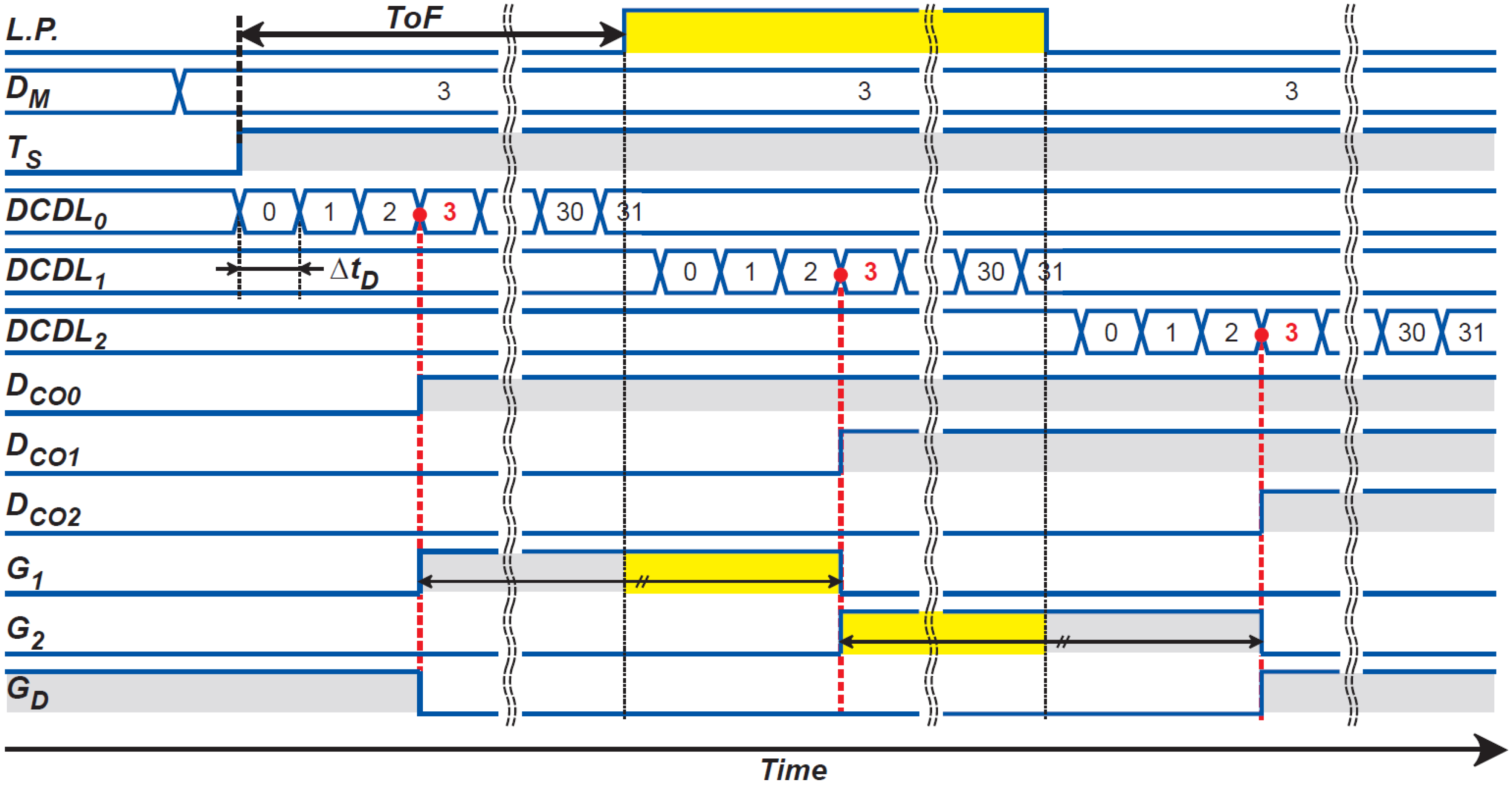
2.3. Coarse-to-Fine ToF Measurements
Figure 6 shows the conceptual operating waveforms of the proposed ToF measurement technique, including the incremental time-to-digital conversion and delta-sigma modulation for coarse and fine ToF measurements. After the coarse conversion, the incremental TDC output produces a coarse estimate of ToF,
. In subsequent fine conversion using the DSM, DTC output produces a waveform of bit-stream and takes two states of
and
. The DSM output is low-pass filtered and down-sampled for decimation, and the fine ToF measurement, or a fine TDC output,
is produced.
Figure 6 shows the filter output behavior when a digital counter (a first-order integrator) is used for the decimation filter. The filter output at the end of fine conversion is expressed as the number of 1’s of the DSM output, and if it is
and the total sampling number is
, the output of fine ToF measurements
is expressed as
takes the value from 0–1. The output using coarse-to-fine cascaded ToF measurements
is given by
or
If and are chosen as and , this coarse-to-fine ToF measurement technique converts the ToF to a -bit digital code as a result of incremental and DSM-based TDC techniques.
4. Implementation and Measurement
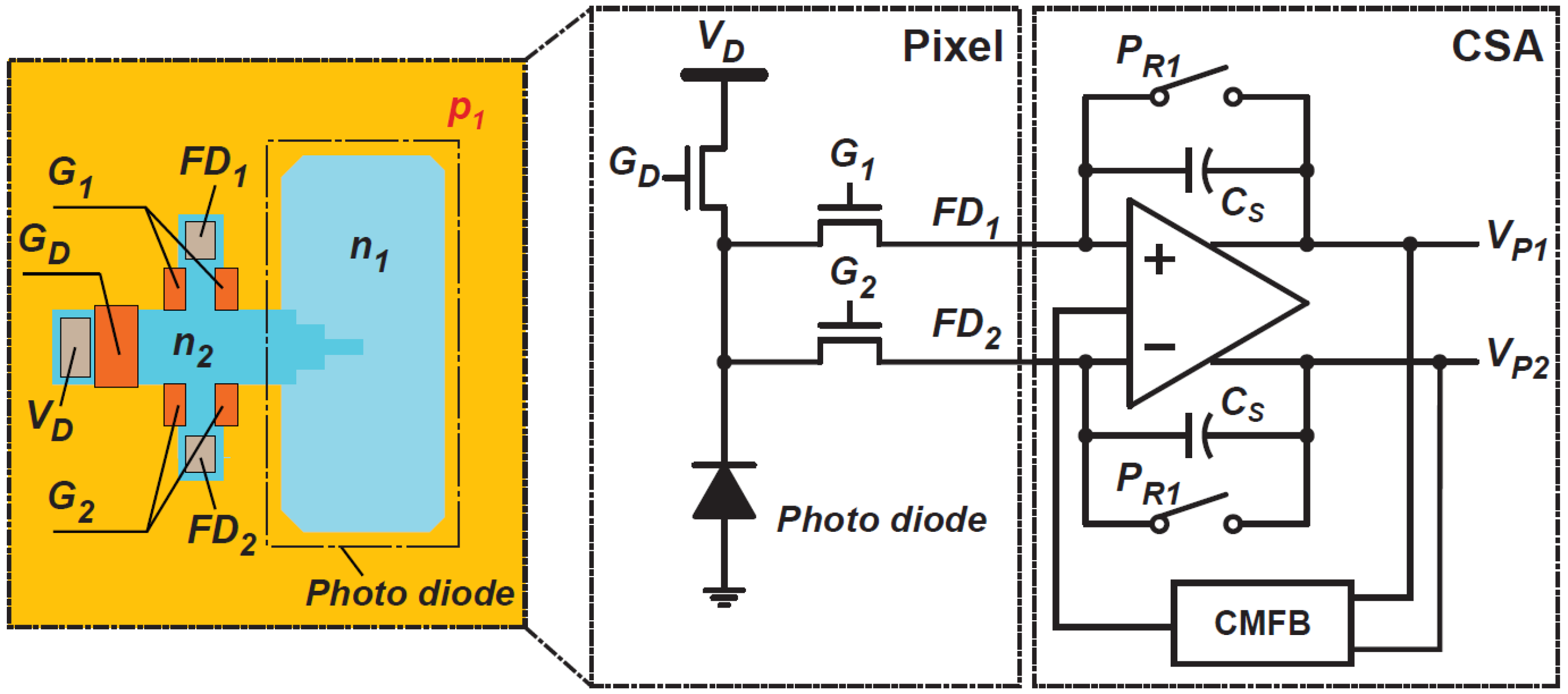
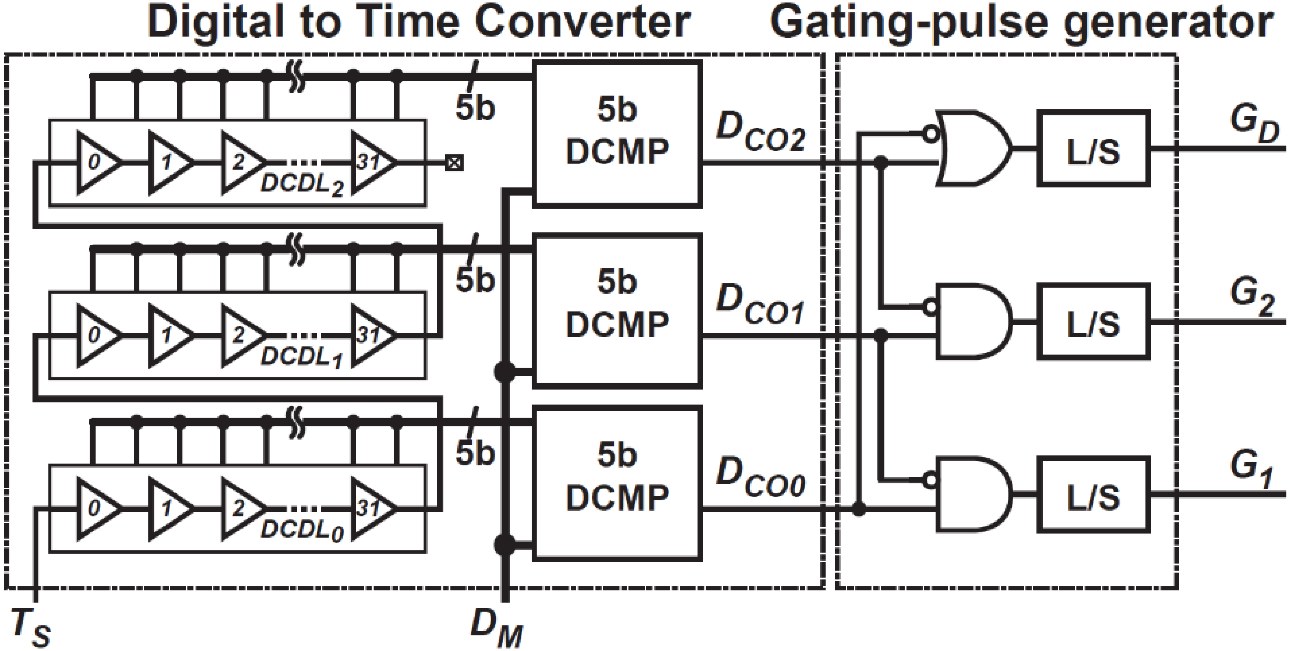
Figure 12 shows a photomicrograph of the prototype chip implemented in 0.11 μm (1P4M) CIS technology. The chip includes 10 × 3 pixels with the demodulator, 10 units of a set consisting of a DCDL, a 5-bit digital comparator (DCMP), a demodulation gate driver, and an APU. The pixel size is 16.8 × 16.8 μm
2, the pitch of the readout circuit channel is 16.8 μm, and the chip core size is approximately 0.232 mm
2. A multiplexer chooses the APU output to evaluate the characteristics of one channel. External components of a field-programmable gate array (FPGA), 1-bit comparator, light pulse generator, digital delay controller, and PC interface are used for implementing the proposed system in
Figure 1.
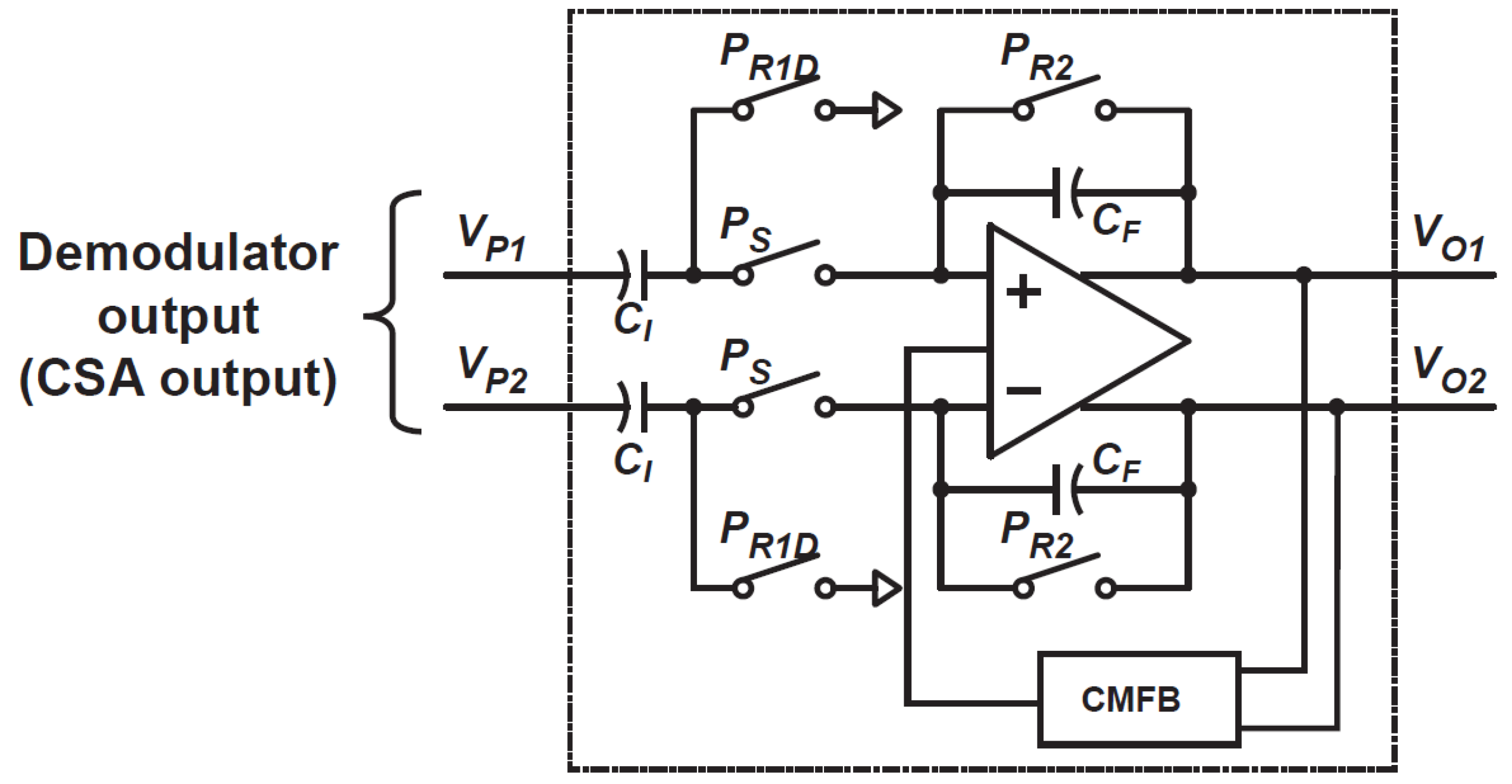
Figure 13 shows the measurement setup for demonstrating the proposed ToF measurement system using the time-domain feedback technique. A specific channel multiplexed from the APU outputs of the implemented chip is connected to an external comparator, and the bit-stream signal output from the comparator is connected to the DPU implemented in the FPGA. The output of the DPU as a 5-bit digital code is fed back to the DCDL of the chip and controls the gating-pulse delay of the demodulator (DM). The FPGA also supplies the light source triggering pulse and operation clock signals for the CSA, APU, and multiplexer of the chip. The DPU implemented in the FPGA covers the function of a counter, a time-offset adder, a decimation filter, and a JTAG interface to PC. The digital output of the chip is finally transferred to the PC for characterizing the implemented ToF sensor chip.
For demonstrating the ToF measurement using the proposed technique with time-domain feedback, a laser diode with a pulse width of 5 ns and a wavelength of 473 nm is used for the light source. The number of light pulses in each DSM oversampling period
is 500. The oversampling frequency used for the DSM is 4.2 MHz. The total ToF measurement time, including both coarse and fine measurements, is 22.4 ms. The total DCDL delay is set to 7 ns with a unit step of 218 ps, and the maximum ToF measurement range is set to 105 cm. A digital delay generator delays and sweeps the trigger pulse of the light source,
, to characterize the response of the implemented ToF measurement system to the pseudo-distance. The maximum number of DTC delay steps
is set to 32 for a 5-bit coarse conversion. The total sampling number
is set to 64 and 66 for the fine DSM conversion.
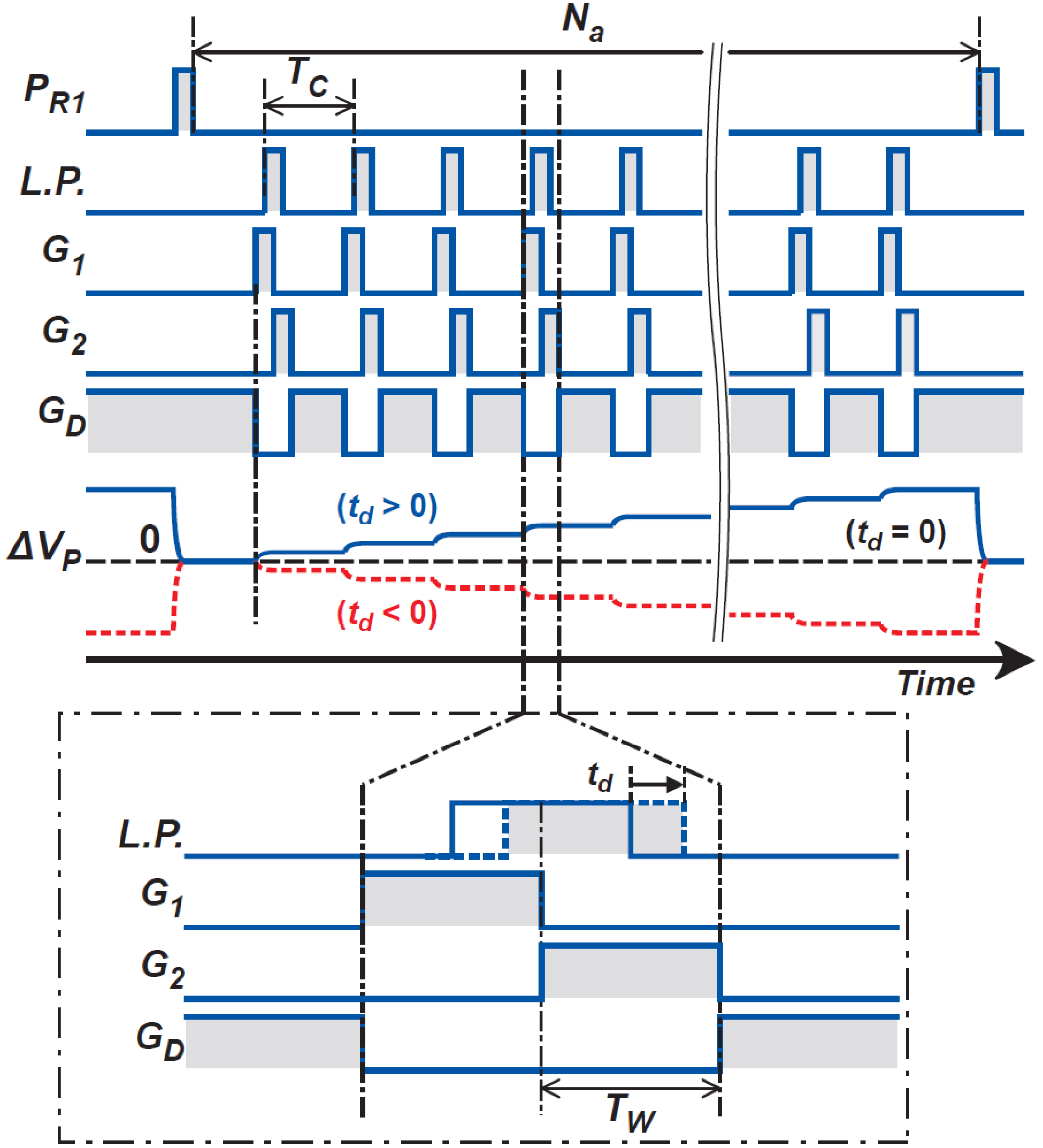
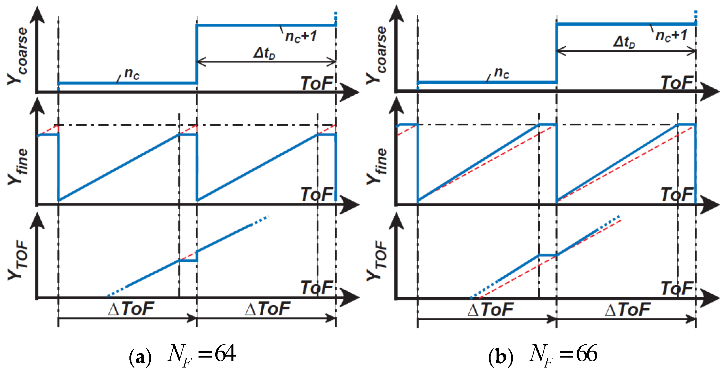
Figure 14 shows a conceptual operating waveform of
,
, and the combined output
for
of 64 (
Figure 14a) and 66 (
Figure 14b). Although
of 64 exactly corresponds to the 6-bit fine ToF-to-digital conversion, it causes time-variant errors at specific codes when the coarse and fine conversion codes are connected. This is because a discontinuous step appears in the linearity curve at the boundary of the maximum
. At this dis-continuous point, a time-variant error occurs, and this extraordinarily worsens the range resolution (or depth noise). This can be avoided by increasing
to be larger than 64. To address this issue,
of 66, corresponding to the 6
+ bits, is also evaluated for improving the depth resolution in
Figure 14b. By increasing
to be 66, the gain of
to ToF is increased by a factor of 66/64 and the linearity curve of
and the resulting
becomes as shown in
Figure 14b. The discontinuous step in the linearity curve of
disappears, and the extraordinal depth noise at the discontinuous point is also reduced at the penalty of a little worse nonlinearity.
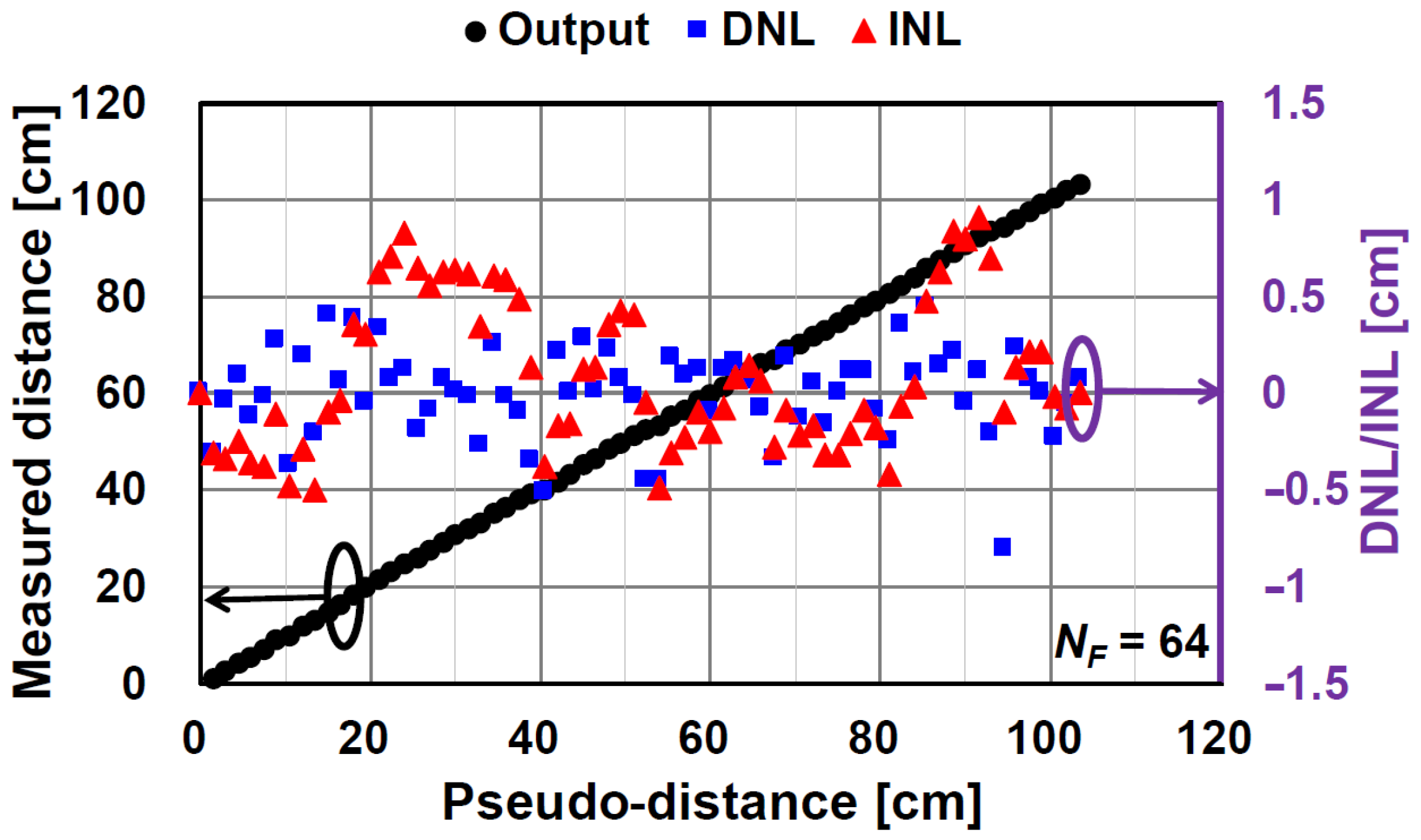
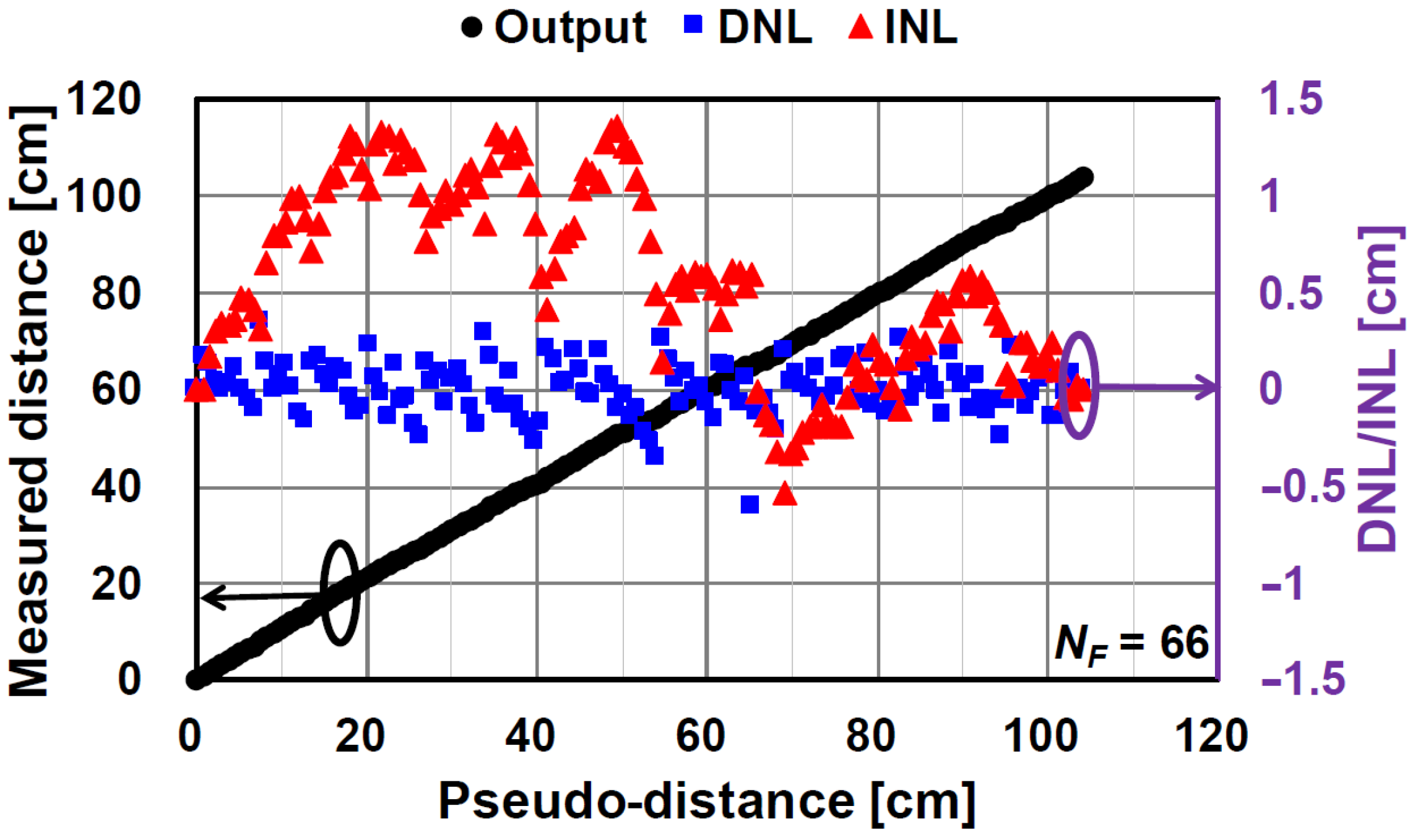
Figure 15 and
Figure 16 show the results of the measured distance, differential nonlinearity (DNL), and integral nonlinearity (INL) for
of 64 and
of 66, respectively. A good linearity is obtained without any corrections for linearity improvements. The maximum INL for the case of
of 64 is +0.9%/−0.47% (+0.94 cm/−0.49 cm) to the entire range of 105 cm. The maximum DNL for
of 64 is +0.43%/−0.76% (+0.45 cm/−0.8 cm) to the entire range of 105 cm. For the case of
= 66, which is used for improving temporal errors, the maximum INL (+1.29%/−0.51% (+1.36 cm/−0.54 cm)) is a little worse than that for
of 64 because the code resolution is not equal to 6 bits. However, the maximum DNL (+0.33%/−0.58% (+0.35 cm/−0.6 cm)) for the
of 66 is even better than
of 64 because the redundancy of the code (
of 66 corresponds to a resolution of 6.044 bits) might improve the nonlinearity at the connecting points of the coarse and fine digital codes.
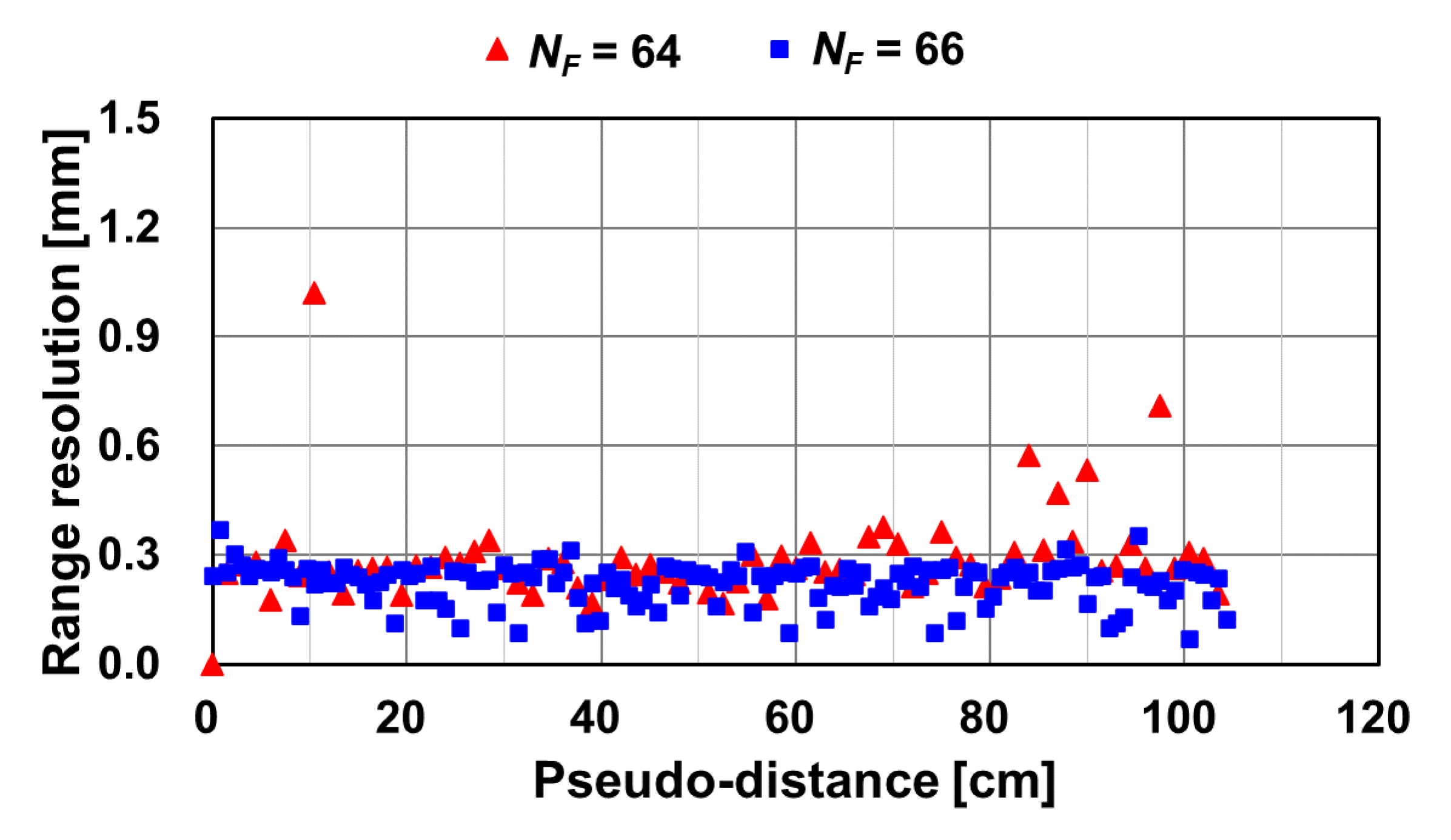
Figure 17 shows the measurement results of the depth resolution to the pseudo-distance. Two cases of fine ToF measurement setting for
of 64 and
of 66 were compared. For
= 64, the range resolution of 0.27 mm (median) is good compared with other indirect ToF sensors in
Table 1. However, at specific points, the range resolution is 3 times worse than its median, and the worst case is 1.02 mm. This extra-ordinal error is because of the temporal variation of nonlinearity at the connection points of the coarse and fine digital code. This problem is solved by increasing the effective number of bits for fine measurement using DSM. By using
of 66, the range resolution (median) is improved from 0.27 mm to 0.24 mm, and the worst value is from 1.02 mm to 0.37 mm. Therefore, the code redundancy for fine ToF measurements might improve the temporal variation of nonlinearity at the connecting points of the coarse and fine digital codes, and the resulting depth resolution is entirely good.
The performance summary of the ToF sensor of this work and a comparison to other works are shown in
Table 1. Because the implemented ToF sensor chip is a preliminary one having only 3(V) × 10(H) pixels and the design specifications are different from each other, this table is not intended for the overall chip performance comparison. With this table, however, the important feature of this work is clarified by the comparison of linearity and range resolution. In general, meeting both high linearity and high range resolution is difficult. A high range resolution needs a high-speed response of the pixel to use shorter light pulse modulation or higher modulation frequency, leading to distortions in the light-pulse waveform, photo-current waveform, and analog demodulation. The proposed technique using the time-domain negative feedback in this work is the best method for simultaneously meeting high linearity (+0.9%/−0.5%) and high range resolution (0.27 mm (median), 0.026% to full range (1.05 m)). Particularly for the comparison with Reference [
26], which demonstrated sub-100 μm resolution, the advantage of this work is the large working range while attaining a good resolution. This feature comes from the proposed coarse-to-fine ToF measurement method, where the range is digitally extended by the incremental DTC and resolved finely with the short pulse width of 5 ns and oversampled noise suppression in the delta-sigma modulation.
Table 2 shows comparison of ToF sensor architectures including this work and two other typical ToF sensor architectures. The indirect ToF sensors using CW (Continuous Wave) and SP (Short Pulse) modulation uses simple analog readout circuits like a source follower. Because of this, it is suitable for implementing large area-array (2D pixel array)-type ToF image sensors. However, the analog readout types have issues of the nonlinearity and stability due to the analog elements like a photo-demodulator and amplifier. Because the role of the indirect ToF pixel is just the demodulation of modulated photo signals, the processing for range calculation and ambient light canceling have to be done by post-processing at an external system. In contrast to the indirect ToF sensors using analog readout circuits, the readout circuits per pixel of the direct ToF sensor using the SPAD and this work are based on digital-processing techniques. Though the readout and processing circuits are relatively complicated when compared with those of the indirect ToF sensors, there is a distinct advantage in its principle for having a high accuracy (high linearity) because of the use of the digitally regulated time reference. The direct ToF sensor using time stamping and the digital ToF sensor using the time-domain feedback technique (this work) use a time-to-digital converter and digital-to-time converter, respectively, for measuring the ToF, and the accuracy (linearity) is dominated by these digital elements, whose accuracy and stability can be much better than the analog counterparts. In these direct ToF sensors, the range calculation and the ambient-light cancellation are self-contained because the digital output is just the ToF itself. The biggest advantage of the direct ToF sensor using SPAD lies in its single-photon sensitivity, and therefore the SPAD-based direct ToF sensors are becoming a key technology for long-distance (>50 m) LiDAR applications. On the other hand, its photon-based processing may cause a difficulty in treating many photons, and the dynamic range is limited by the processing speed of the time-stamping of a photon. Therefore, the SPAD-based direct ToF sensors are not always the best solution for distance measurements for a few meters and with strong signals. The per-pixel readout circuits of the digital ToF sensor using the time-domain feedback are more complicated than that of the indirect ToF sensors but less complicated than that of the SPAD-based direct ToF sensors. The ambient light canceling is done by an analog fully differential charge-sensitive amplifier (CSA) during the demodulation process. While the dynamic range is limited by the full well capacity (FWC) of the fully differential CSA, the use of oversampling done in the delta-sigma modulation is effective for extending the dynamic range and reducing the influence of shot noise, because the integration of the sampled CSA outputs in the integrator has an effect of improving the shot-noise-limited signal-to-noise ratio. As a result, high range resolution (0.27 mm @ 0–1.05 m) is attained in this work. Because of the complicated analog and digital circuits per pixel, the proposed circuits architecture is suitable only for linear-array (1D) ToF image sensors.
5. Conclusions
A high-linearity high-depth resolution ToF linear-array digital image sensor using time-domain feedback that works as incremental gating-pulse delay feedback and DSM for coarse and fine ToF measurements, respectively, has been presented. The coarse ToF measurement uses time-domain feedback using the gating-pulse delay generated by a 5-bit DTC. The fine ToF measurement uses a first-order DSM for time-domain bit-stream feedback and oversampling signal processing for attaining high piecewise linearity and low depth noise (high depth resolution).
For a demonstration of the proposed system, a prototype sensor chip was implemented with a 0.11 μm (1P4M) CIS process. The chip contains a DTC, pulse generator, demodulation pixels, APU, and multiplexer. The other necessary functional blocks, such as a comparator, the DPU, timing controller, light source, and digital delay generator, are implemented using discrete components or an FPGA. The ToF measurement system produces an 11-bit fully digital output with a measurement cycle time of 22 ms. The prototype ToF system observed good linearity of +0.9%/−0.47%. An excellent range resolution of 0.24 mm (best case) for the range of 0–1.05 m is demonstrated. The residual nonlinearity is predominantly because of the deviation of the delay elements in the implemented DTC, which will be improved by introducing a precise DTC.


