Fabrication and Characterization of a High-Performance Multi-Annular Backscattered Electron Detector for Desktop SEM †


Abstract
:1. Introduction
2. Design Concept
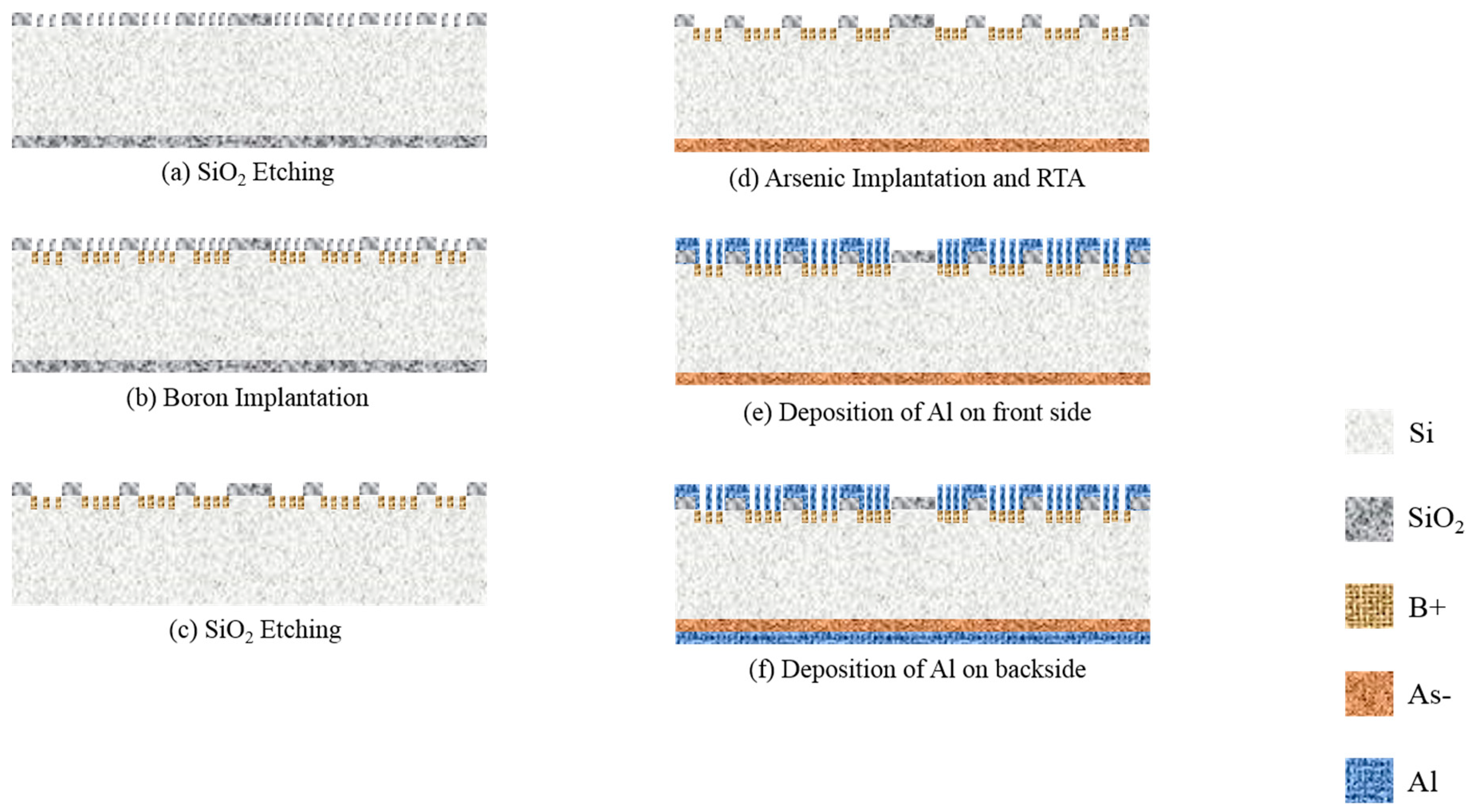
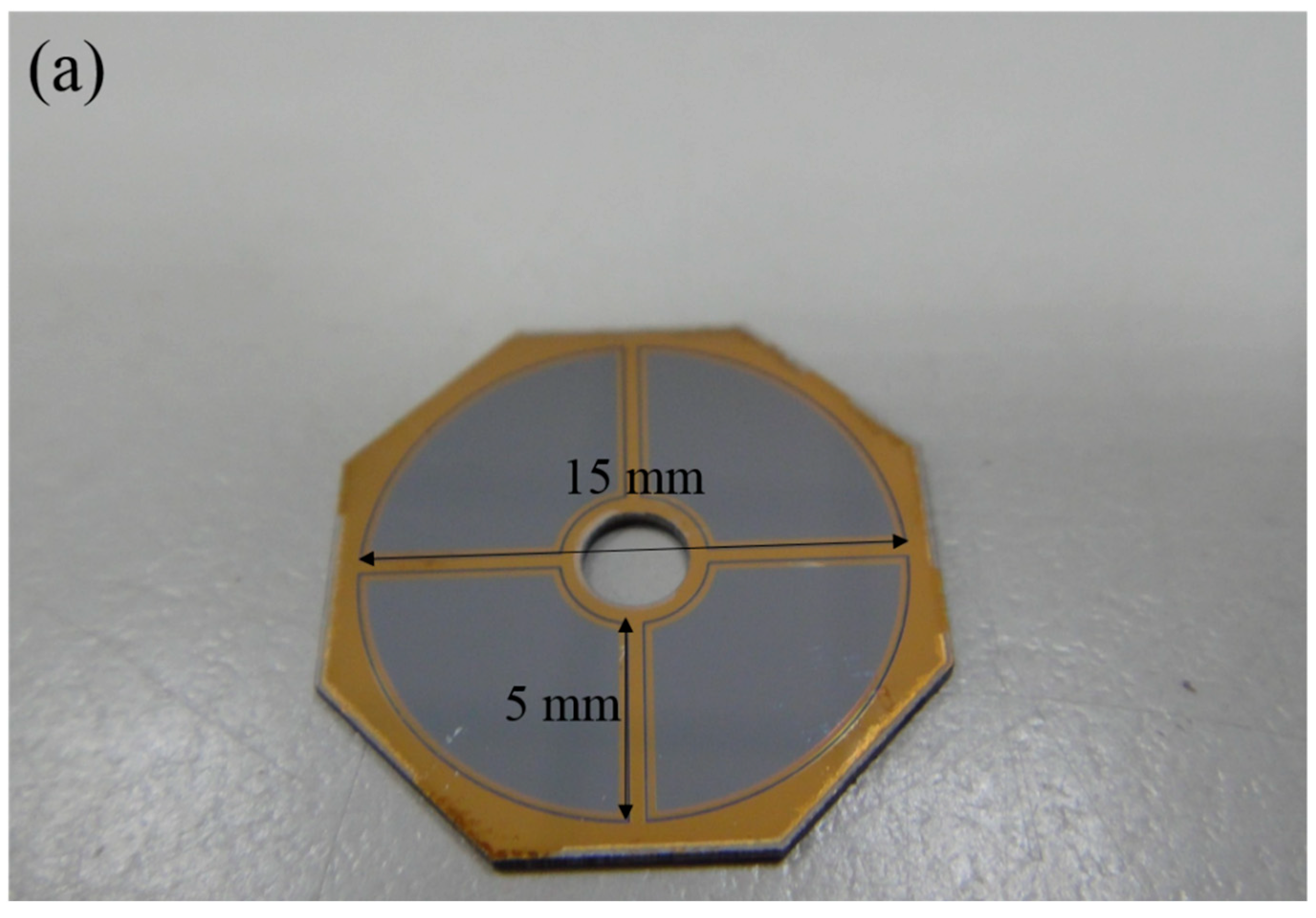
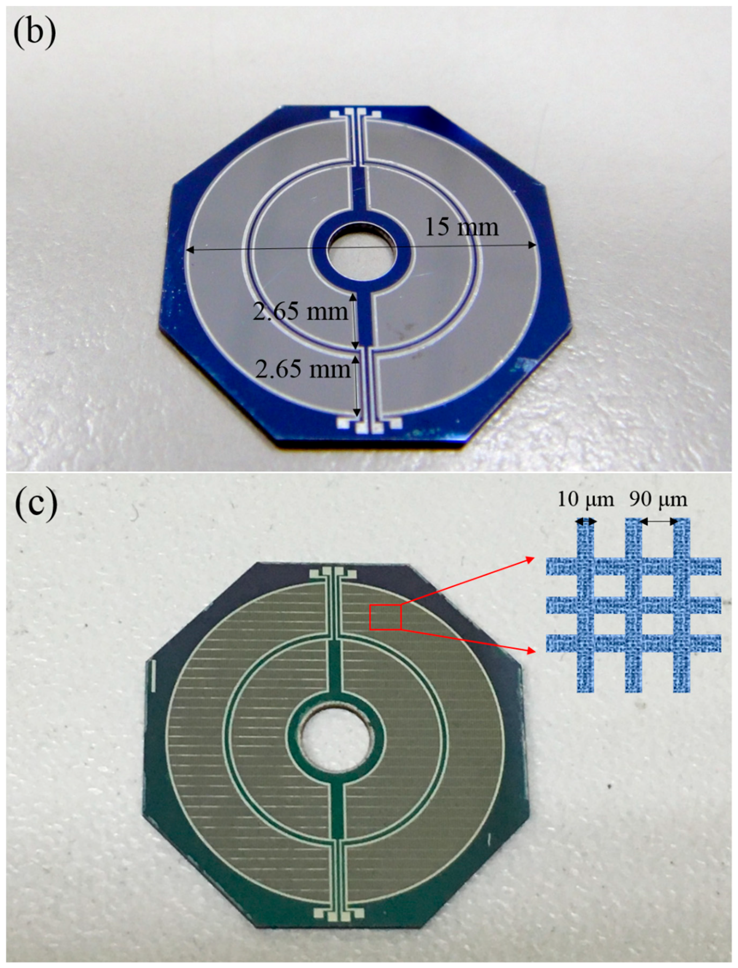
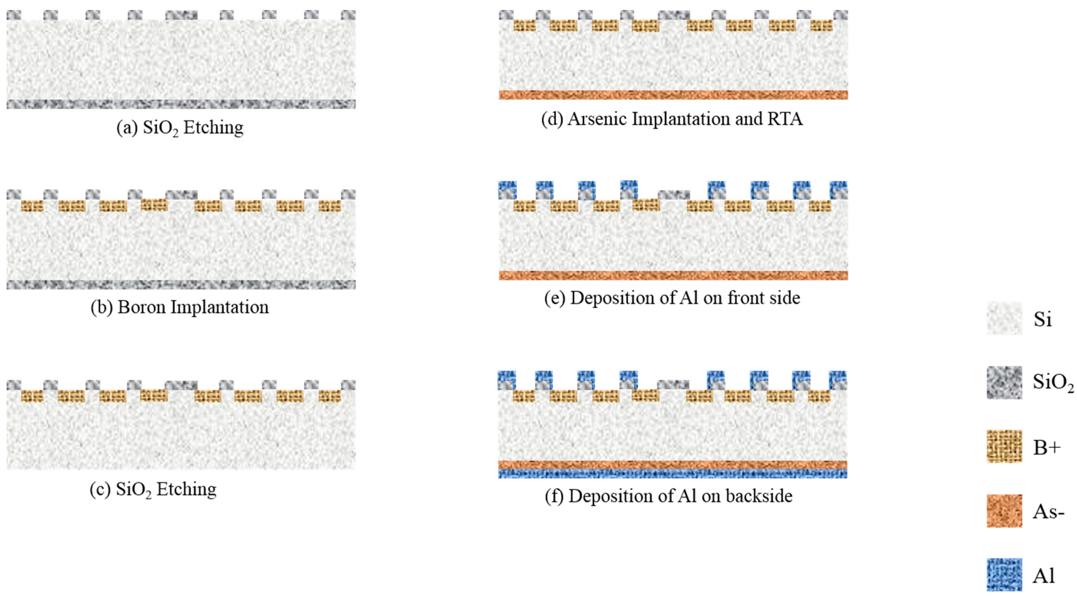
3. Fabrication
4. Results
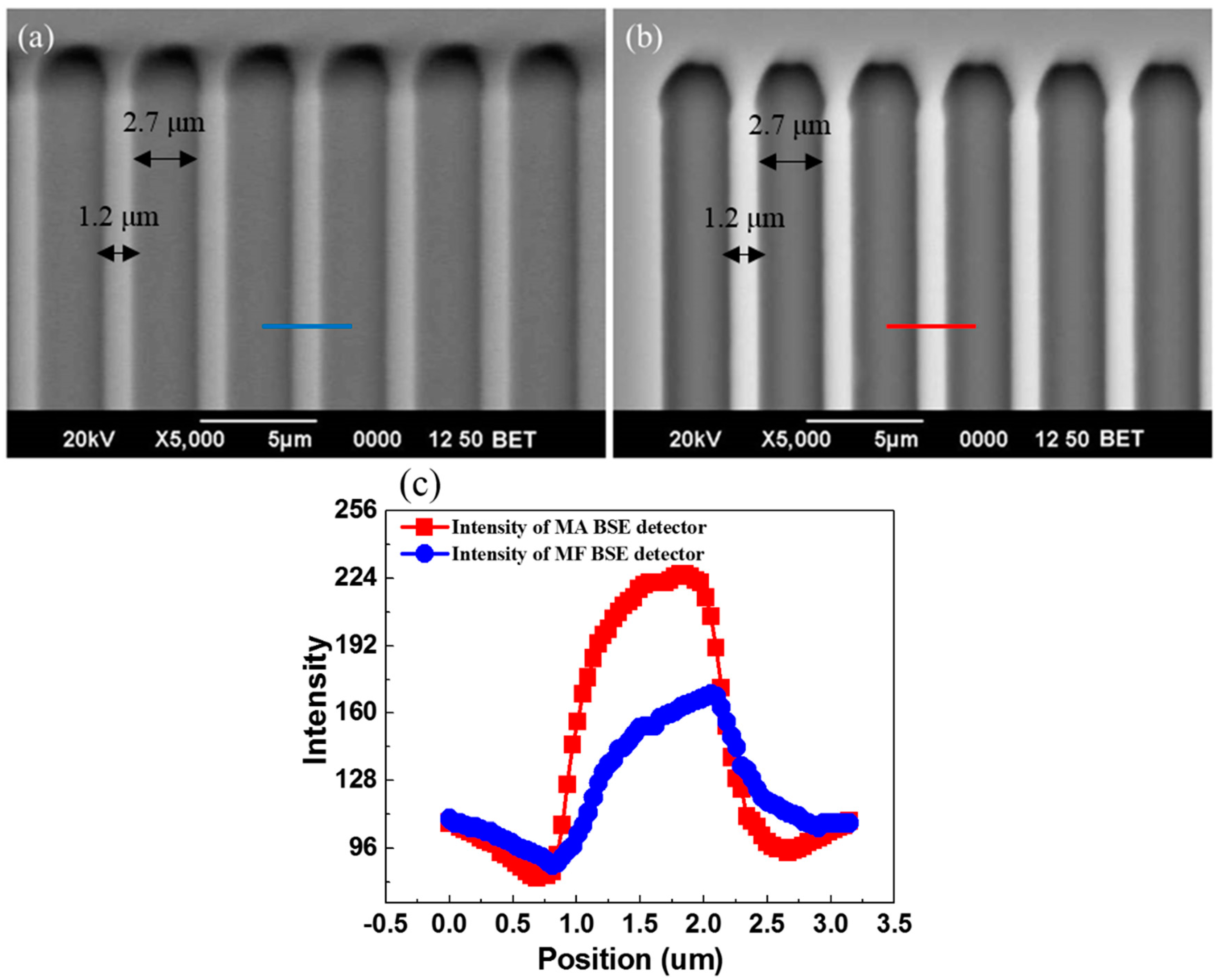
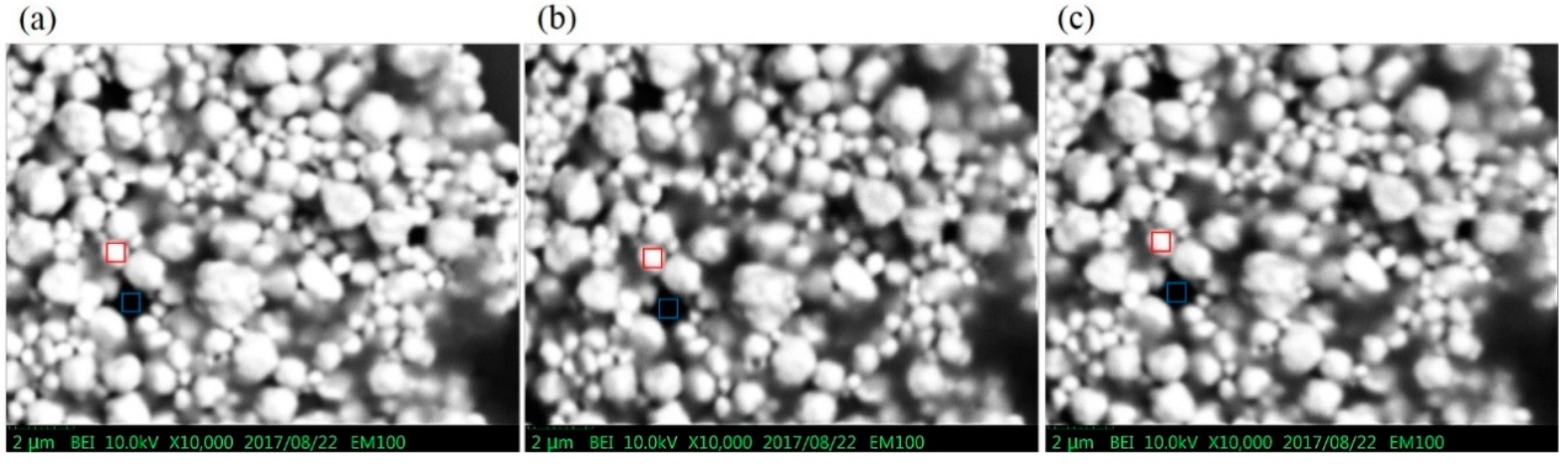
4.1. Surface Topography Contrast
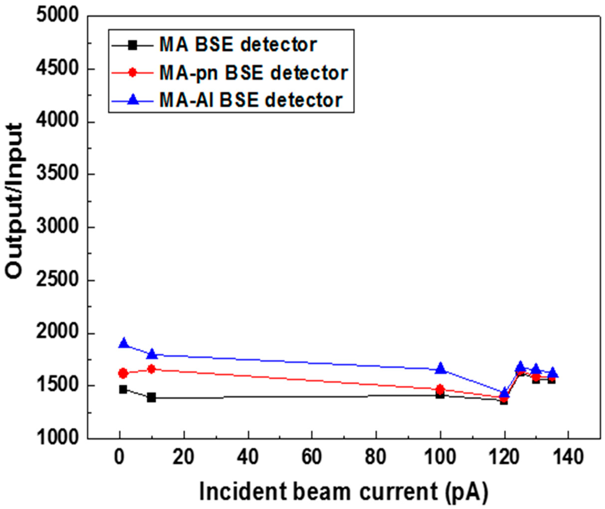
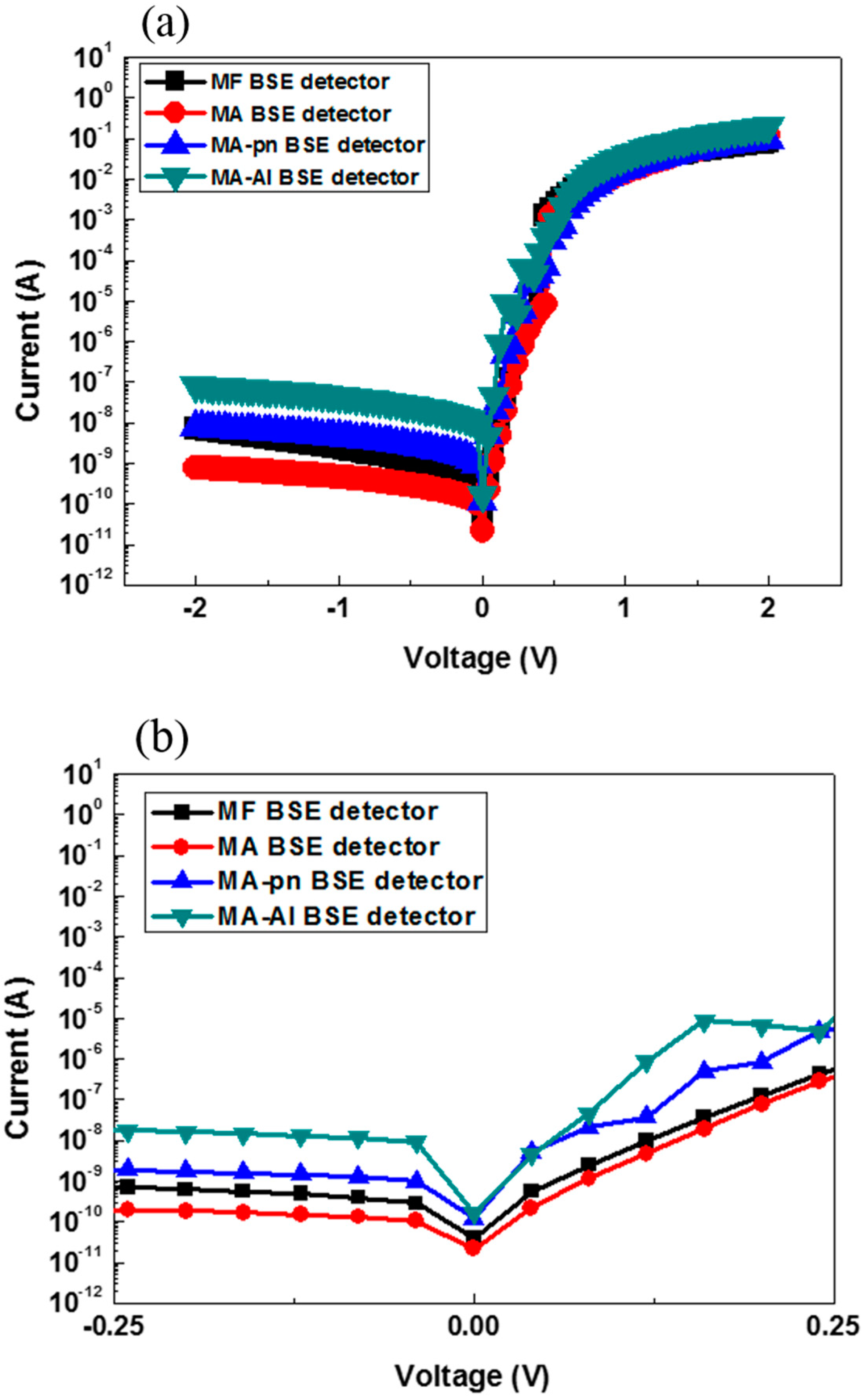
4.2. I–V Characteristics
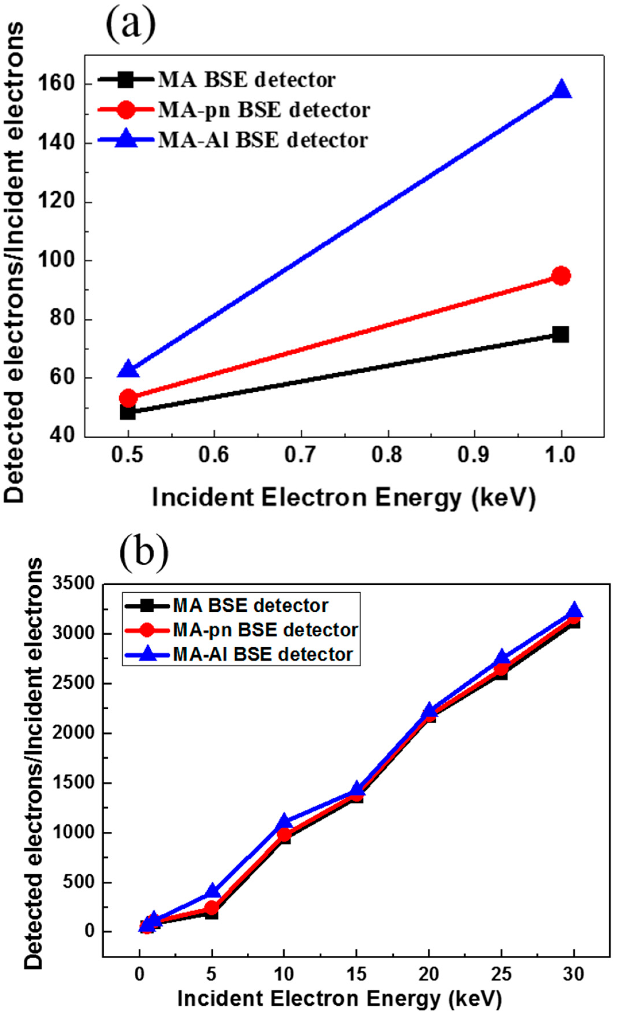
4.3. Effective Gain of Detectors for Electron Energy Lower Than 15 keV
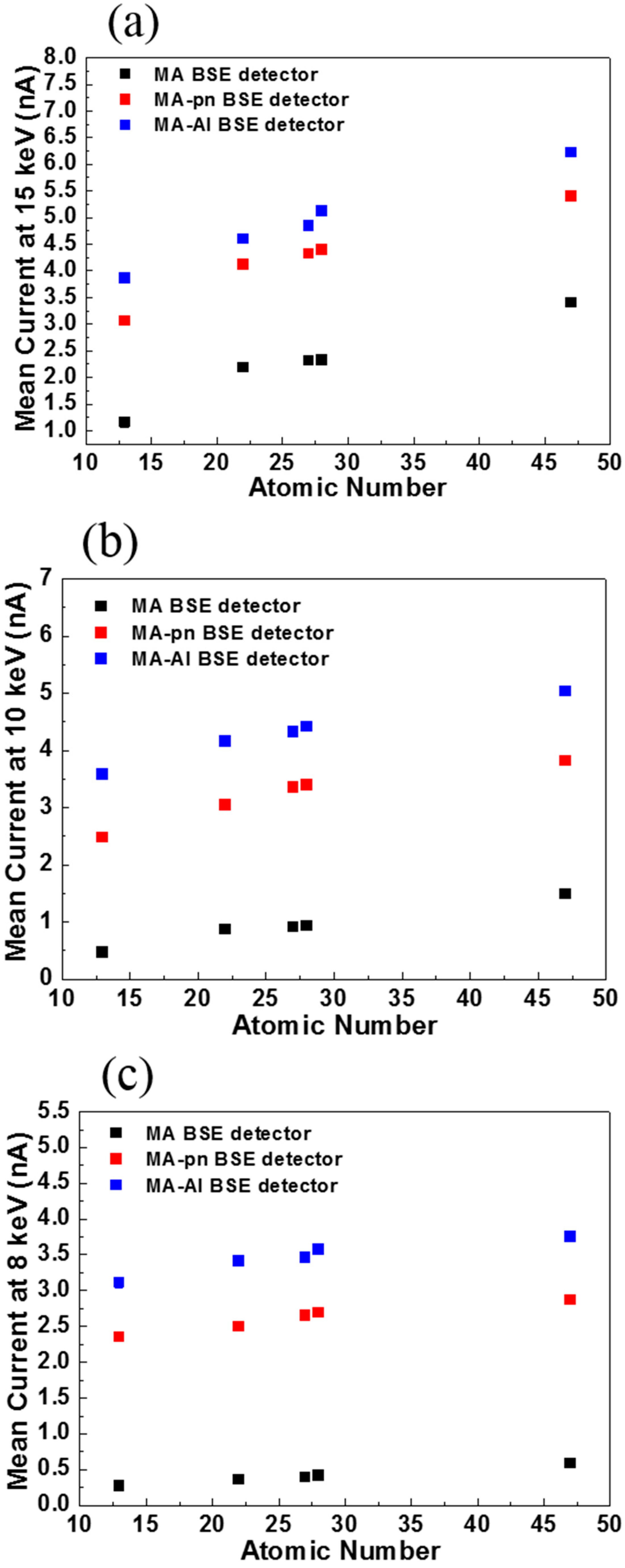
4.4. Sensitivity of Atomic Number
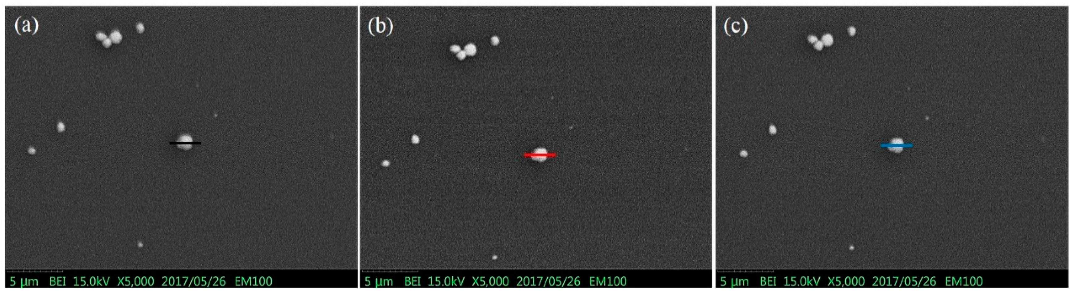
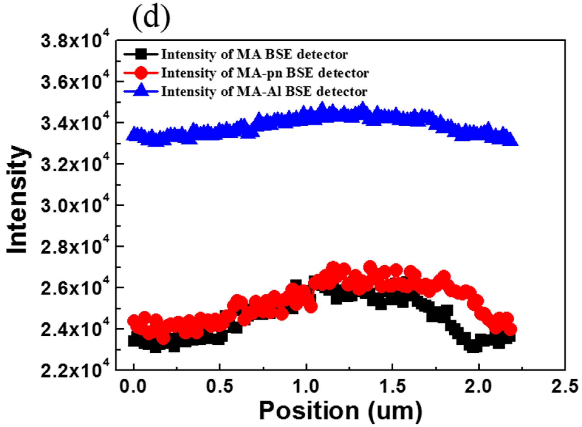
4.5. BEI Contrast
5. Conclusions
Author Contributions
Acknowledgments
Conflicts of Interest
References
- Perovic, D.D.; Castell, M.R.; Howie, A.; Lavoie, C.; Tiedje, T.; Cole, J.S.W. Field-emission SEM imaging of compositional and doping layer semiconductor superlattices. Ultramicroscopy 1995, 58, 104–113. [Google Scholar] [CrossRef]
- Zhou, W.; Wang, Z.L. Scanning Microscopy for Nanotechnology: Techniques and Applications; Springer: Berlin/Heidelberg, Germany, 2007. [Google Scholar]
- Carr, K.E. Applications of scanning electron microscopy in biology. Int. Rev. Cytol. 1971, 30, 183–255. [Google Scholar] [PubMed]
- Echlin, P. The applications of scanning electron microscopy to biological research. Philos. Trans. R. Soc. B 1971, 261, 51–59. [Google Scholar] [CrossRef]
- Buss, H. Scanning electron microscopy in pathology. Beiträge zur Pathologie 1973, 148, 315–339. [Google Scholar] [CrossRef]
- Munden, A.V.; Walker, D.Y. A silicon detector for the Stereoscan scanning electron microscope. J. Phys. E Sci. Instrum. 1973, 6, 916. [Google Scholar] [CrossRef]
- Stephen, J.; Smith, B.J.; Marshall, D.C.; Wittam, E.M. Applications of a semiconductor backscattered electron detector in a scanning electron microscope. J. Phys. E Sci. Instrum. 1975, 8, 607. [Google Scholar] [CrossRef]
- Thornton, P.R. Scanning Electron Microscopy; Chapman and Hall: London, UK, 1968; p. 85. [Google Scholar]
- Robinson, V.N.E. The construction and uses of an efficient backscattered electron detector for scanning electron microscopy. J. Phys. Instrum. 1974, 7, 650–652. [Google Scholar] [CrossRef]
- Wells, O.C. Backscattered electron image (BSI) in the scanning electron microscope (SEM). Scanning Electron Microsc. 1977, 1, 747–771. [Google Scholar]
- Reimer, L.; Tollkamp, C. Measuring the backscattering coefficient and secondary electron yield inside a scanning electron microscope. Scanning 1980, 3, 35–39. [Google Scholar] [CrossRef]
- Robinson, V.N.E. Imaging with backscattered electrons in a scanning electron microscope. Scanning 1980, 3, 15–26. [Google Scholar] [CrossRef]
- Ball, M.D.; Amor, M.P.; Lamb, H.J. The measurement of atomic number and composition in an SEM using backscattered detectors. J. Microsc. 1981, 124, 57–68. [Google Scholar] [CrossRef]
- Kaczmarek, D.; Czyżewski, Z.; Hejna, J.; Radzimski, Z. Investigation of the surface topography using backscattered electron signal. Scanning 1987, 9, 109–116. [Google Scholar] [CrossRef]
- Kaczmarek, D.; Czyzewski, Z. Signal of backscattered electrons from multiple marks in dependence on mark profile. Scanning Microsc. 1988, 2, 1273–1281. [Google Scholar]
- Kaczmarek, D. Backscattered electrons topographic mode problems in the scanning electron microscope. Scanning Microsc. 1998, 12, 161–169. [Google Scholar]
- Fritz, G.S.; Fresser, H.S.; Prins, F.E.; Kern, D.P. Lateral pn-junctions as a novel electron detector for microcolumn systems. J. Vac. Sci. Technol. B Microelectron. Nanometer Struct. 1999, 17, 2836–2839. [Google Scholar] [CrossRef]
- Sakic, A.; van Veen, G.; Kooijman, K.; Vogelsang, P.; Scholtes, T.L.; de Boer, W.B.; Derakhshandeh, J.; Wien, W.H.; Milosavljevic, S.; Nanver, L.K. High-efficiency silicon photodiode detector for sub-kev electron microscopy. IEEE Trans. Electron Devices 2012, 59, 2707–2714. [Google Scholar] [CrossRef]
- Zaluzec, N.J. Analytical formulae for calculation of X-ray detector solid angles in the scanning and scanning/transmission analytical electron microscope. Microsc. Microanal. 2014, 20, 1318–1326. [Google Scholar] [CrossRef] [PubMed]
- Reimer, L. Scanning Electron Microscopy: Physics of Image Formation and Microanalysis; Springer: Berlin/Heidelberg, Germany, 1998. [Google Scholar]
- Šakić, A.; Nanver, L.K.; Scholtes, T.L.; Heerkens, C.T.; Knežević, T.; Van Veen, G.; Kooijman, K.; Vogelsang, P. Boron-layer silicon photodiodes for high-efficiency low-energy electron detection. Solid-State Electron. 2011, 65, 38–44. [Google Scholar] [CrossRef]
- Huang, S.H.; Wang, W.J.; Chang, C.S.; Hwu, Y.K.; Tseng, F.G.; Kai, J.J.; Chen, F.R. The fabrication and application of Zernike electrostatic phase plate. J. Electron Microsc. 2006, 55, 273–280. [Google Scholar] [CrossRef] [PubMed]


© 2018 by the authors. Licensee MDPI, Basel, Switzerland. This article is an open access article distributed under the terms and conditions of the Creative Commons Attribution (CC BY) license (http://creativecommons.org/licenses/by/4.0/).
Share and Cite
Lin, W.-R.; Chuang, Y.-J.; Lee, C.-H.; Tseng, F.-G.; Chen, F.-R. Fabrication and Characterization of a High-Performance Multi-Annular Backscattered Electron Detector for Desktop SEM. Sensors 2018, 18, 3093. https://doi.org/10.3390/s18093093
Lin W-R, Chuang Y-J, Lee C-H, Tseng F-G, Chen F-R. Fabrication and Characterization of a High-Performance Multi-Annular Backscattered Electron Detector for Desktop SEM. Sensors. 2018; 18(9):3093. https://doi.org/10.3390/s18093093
Chicago/Turabian StyleLin, Wei-Ruei, Yun-Ju Chuang, Chih-Hao Lee, Fan-Gang Tseng, and Fu-Rong Chen. 2018. "Fabrication and Characterization of a High-Performance Multi-Annular Backscattered Electron Detector for Desktop SEM" Sensors 18, no. 9: 3093. https://doi.org/10.3390/s18093093
APA StyleLin, W.-R., Chuang, Y.-J., Lee, C.-H., Tseng, F.-G., & Chen, F.-R. (2018). Fabrication and Characterization of a High-Performance Multi-Annular Backscattered Electron Detector for Desktop SEM. Sensors, 18(9), 3093. https://doi.org/10.3390/s18093093