CMOS Capacitive Fingerprint Sensor Based on Differential Sensing Circuit with Noise Cancellation


Abstract
:1. Introduction
2. Capacitive Fingerprint Sensing Methods
3. Proposed Differential Sensing Technique
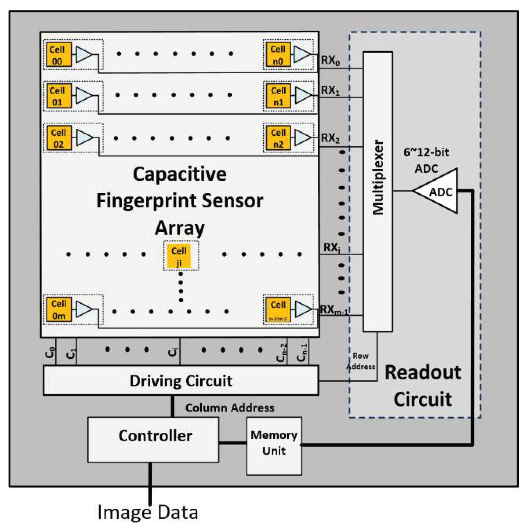
3.1. Differential Sensing Architecture
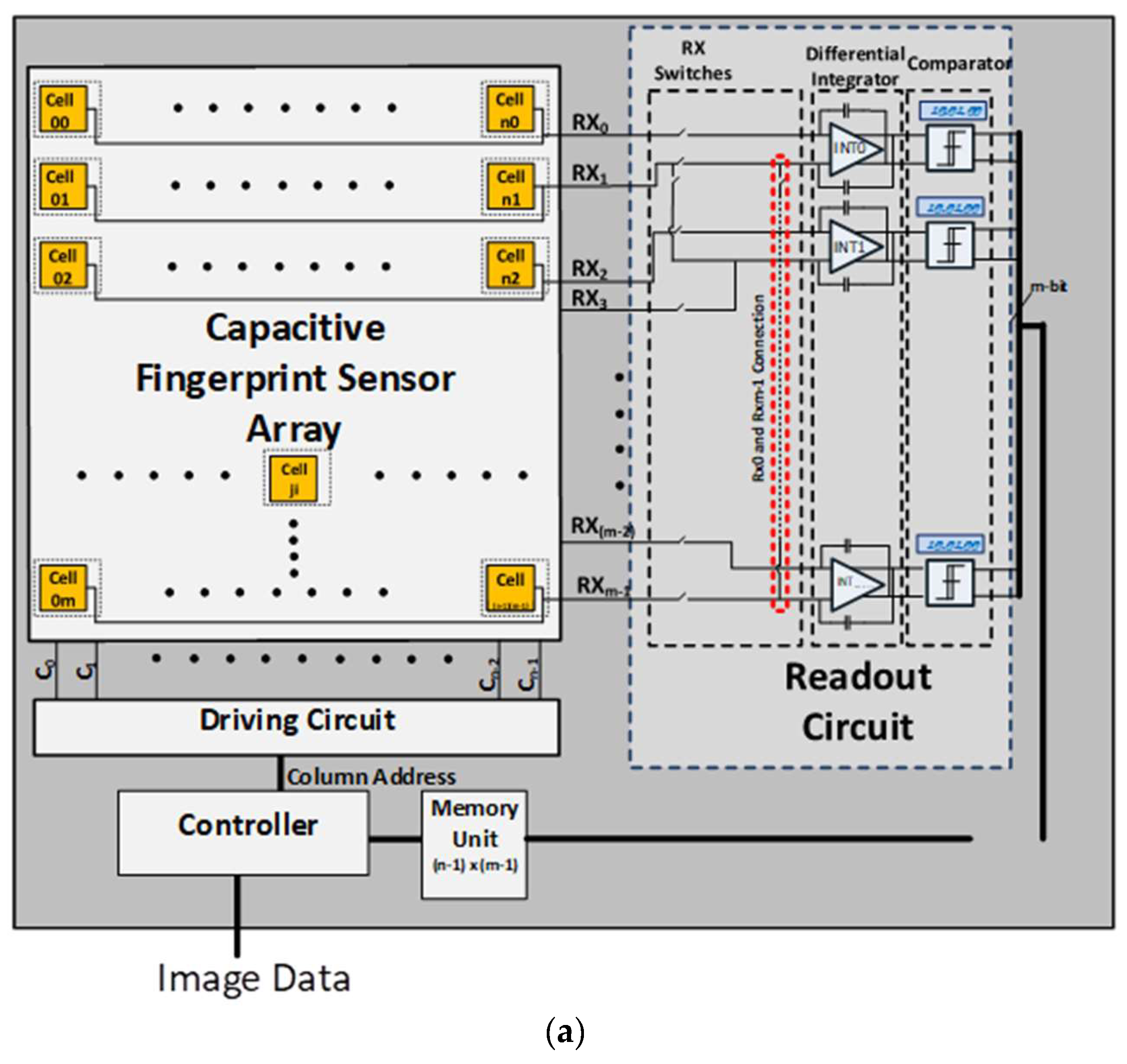
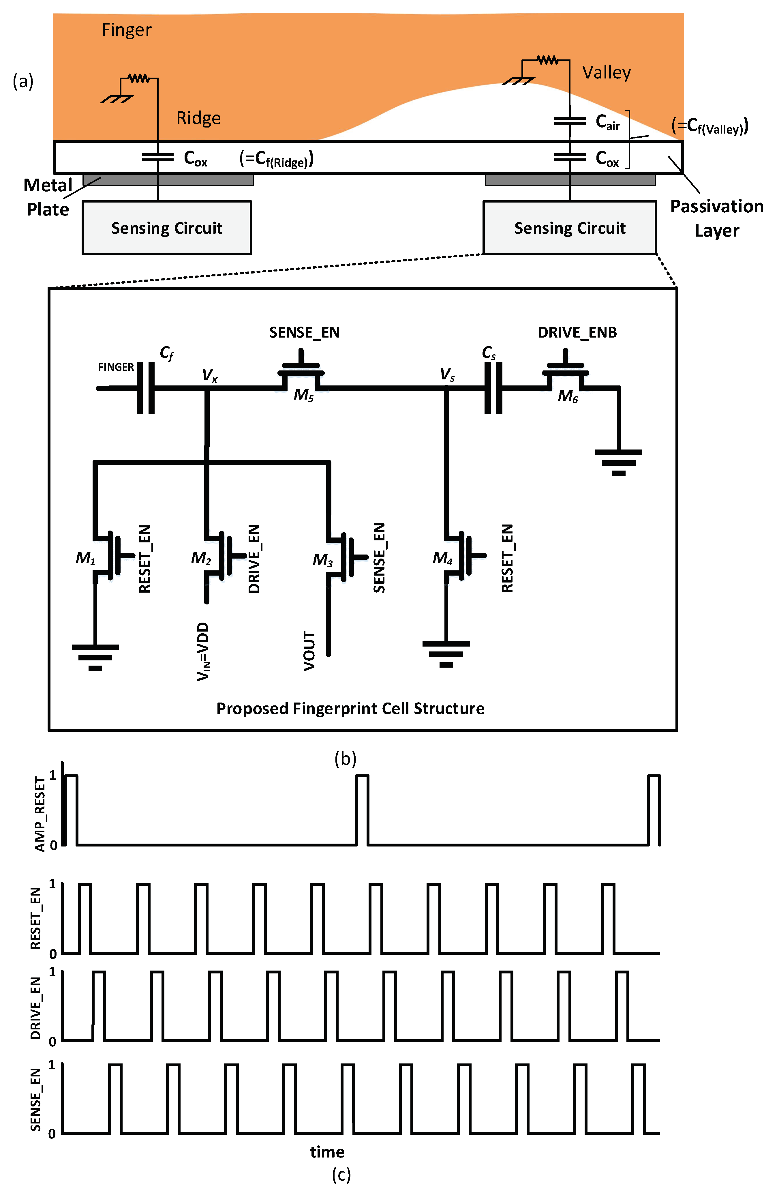
3.2. Proposed Fingerprint Cell Structure
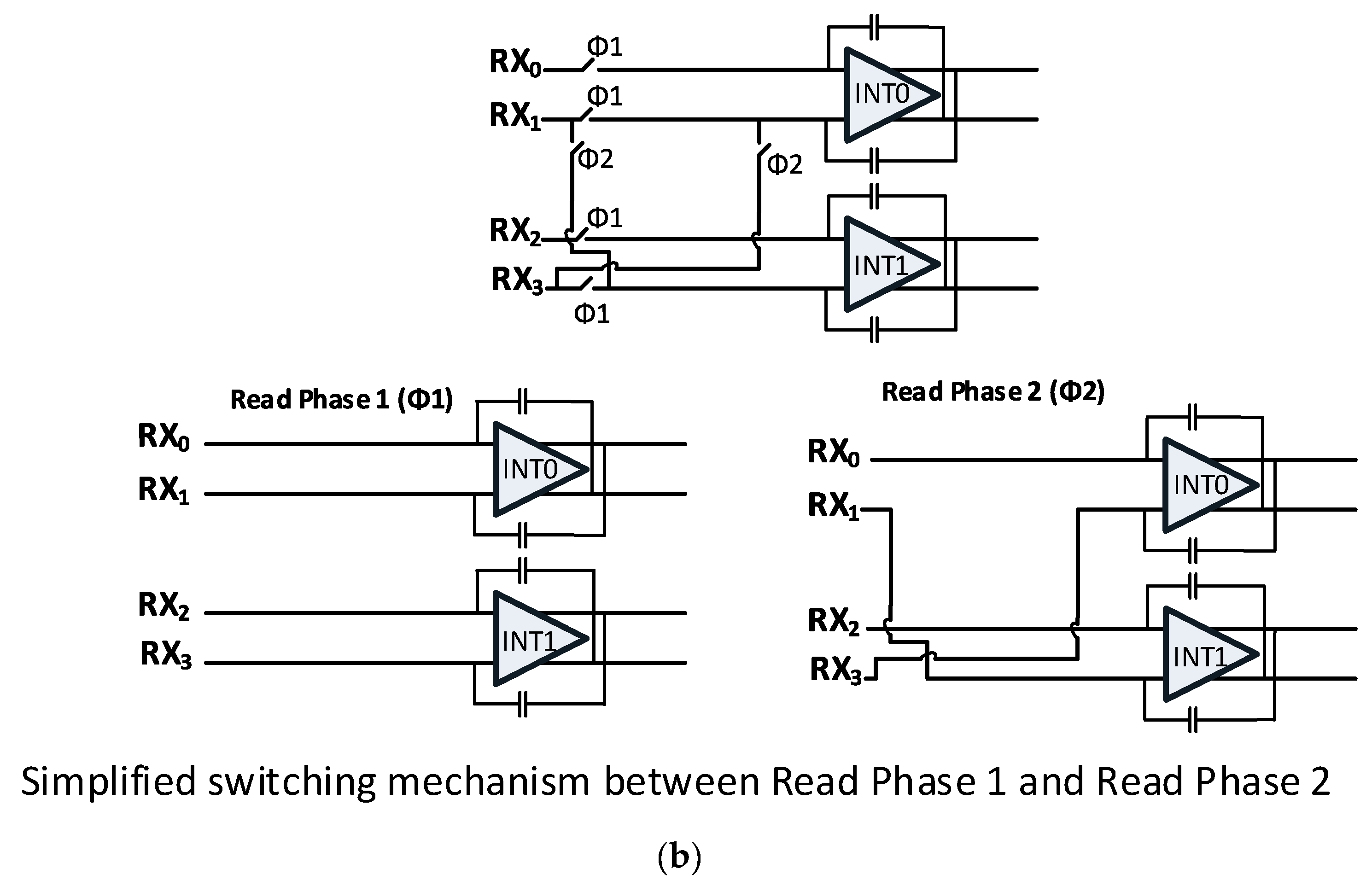
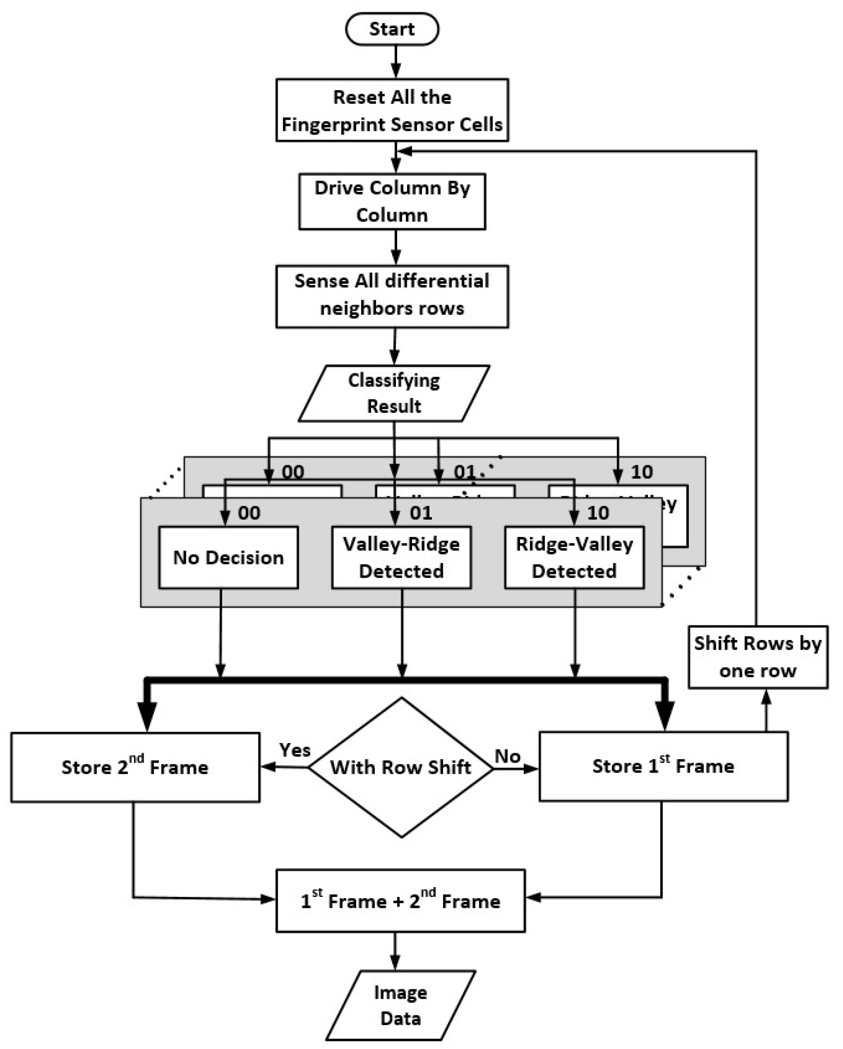
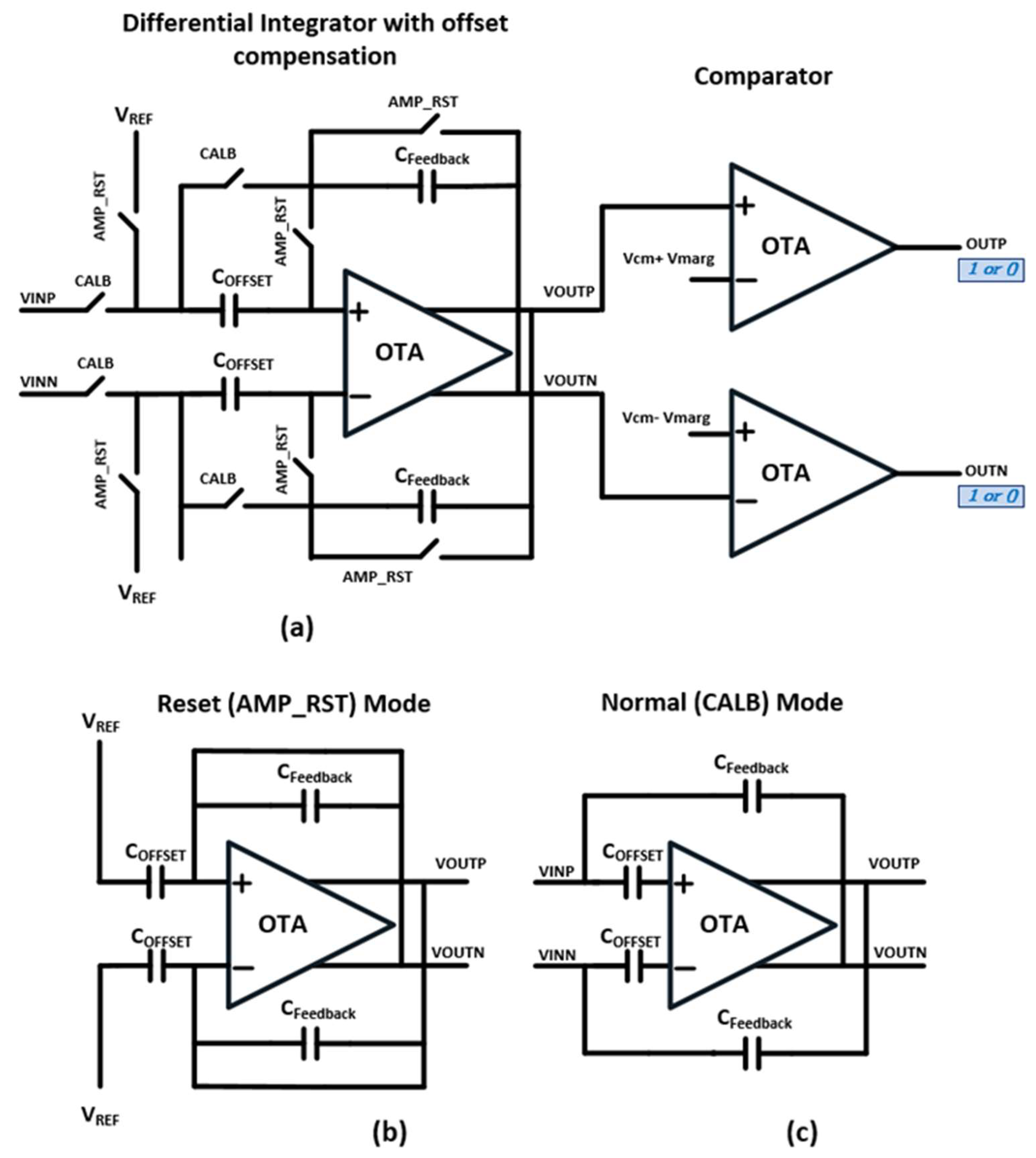
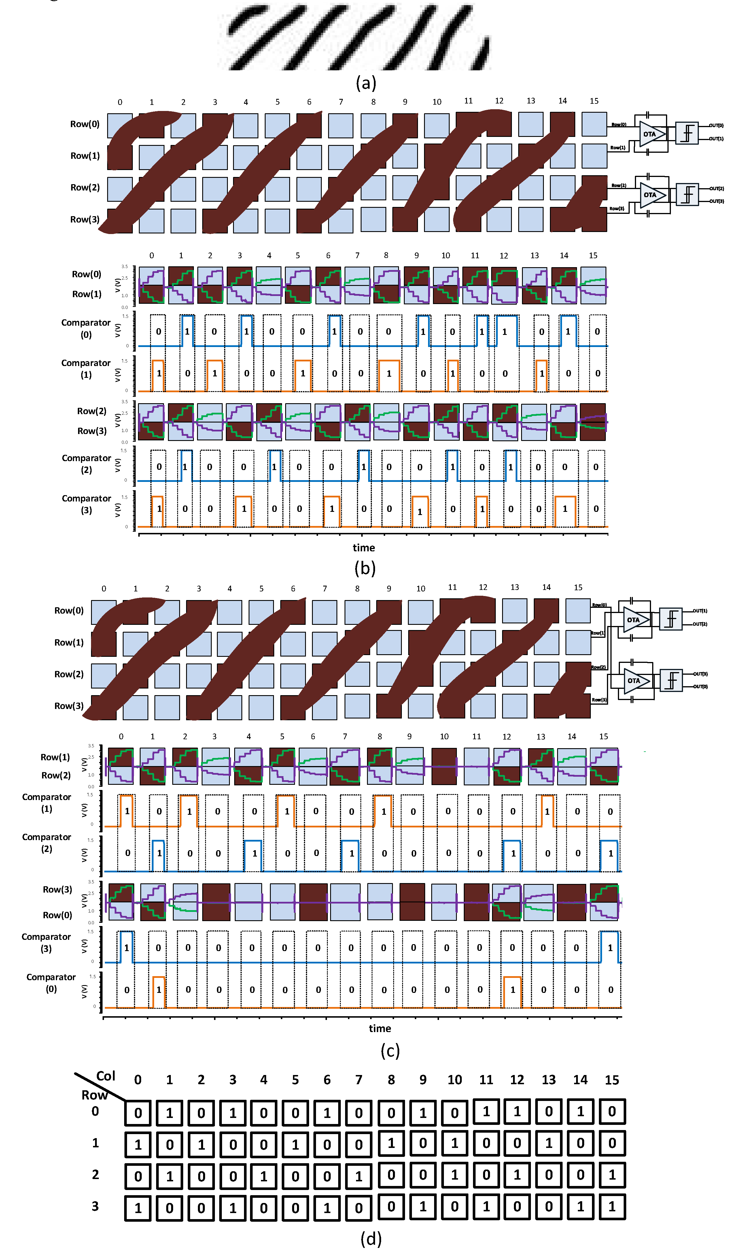
3.3. Parallel Readout Circuit Using Differential Integrators
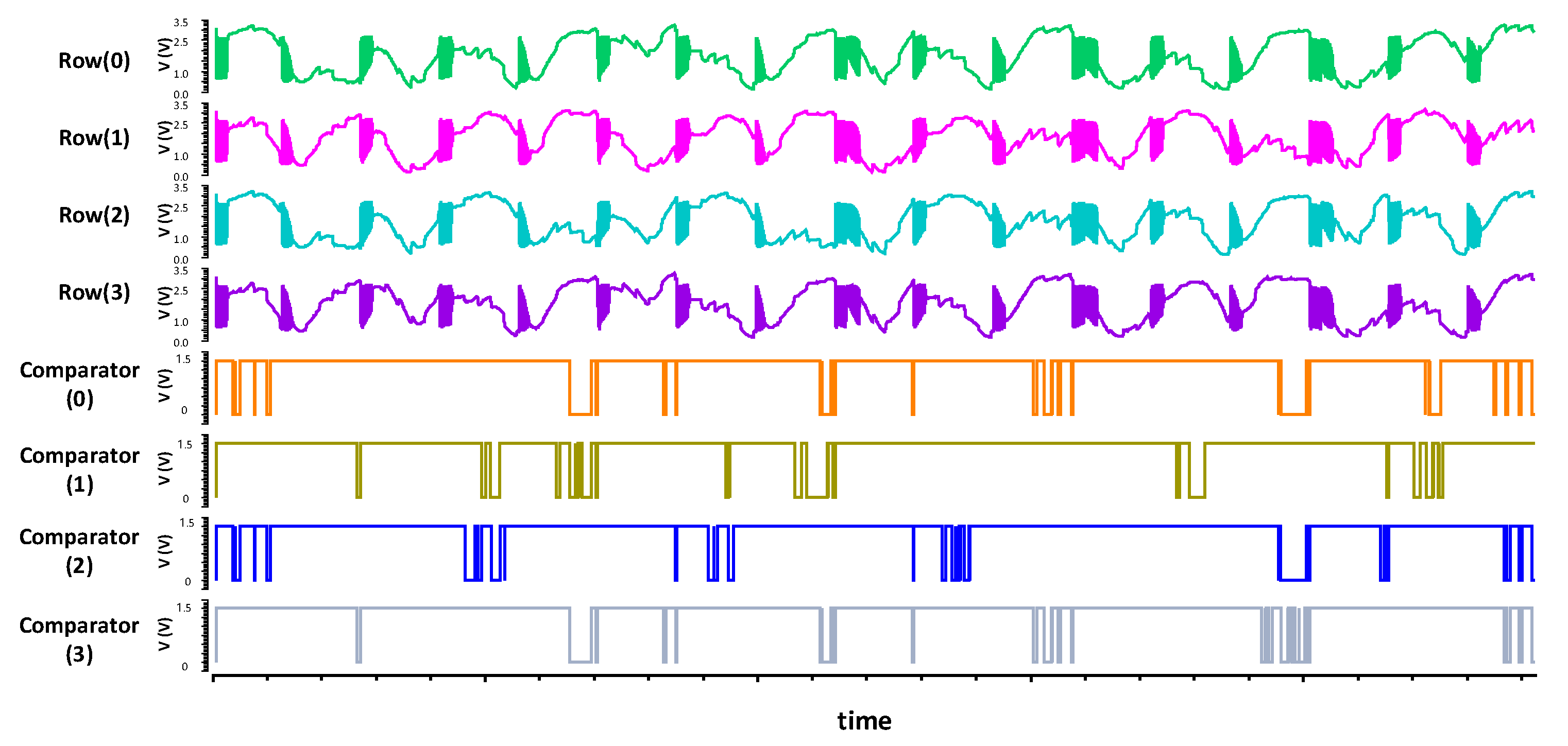
4. Experimental Results
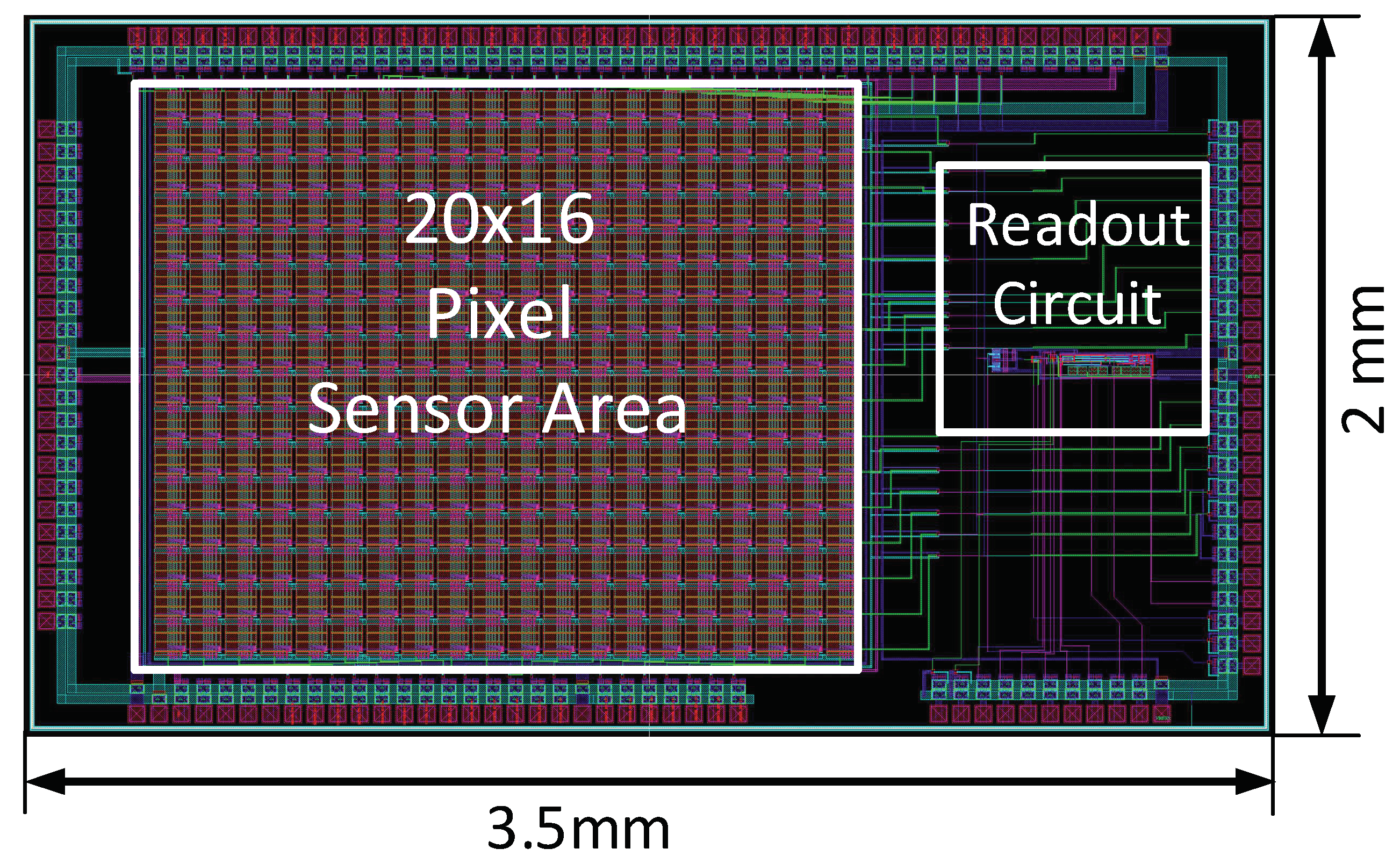
4.1. Implementation of Sensor Chip
4.2. Sensitivity Performance Comparison
5. Conclusions
Author Contributions
Funding
Conflicts of Interest
References
- Kantarci, B.; Erol-Kantarci, M.; Schuckers, S. Towards secure cloud-centric internet of biometric things. In Proceedings of the 2015 IEEE 4th International Conference on Cloud Networking (CloudNet), Niagara Falls, ON, Canada, 5–7 October 2015; pp. 81–83. [Google Scholar]
- Karimian, N.; Wortman, P.A.; Tehranipoor, F. Evolving authentication design considerations for the Internet of Biometric Things (IoBT). In Proceedings of the 2016 International Conference on Hardware/Software Codesign and System Synthesis (CODES + ISSS), Pittsburgh, PA, USA, 2–7 October 2016; pp. 1–10. [Google Scholar]
- Al-alem, F.; Alsmirat, M.A.; Al-Ayyoub, M. On the Road to the Internet of Biometric Things: A Survey of Fingerprint Acquisition Technologies and Fingerprint Databases. In Proceedings of the 2016 IEEE/ACS 13th International Conference of Computer Systems and Applications (AICCSA), Agadir, Morocco, 29 November–2 December 2016. [Google Scholar]
- Ramotowski, R. Lee and Gaensslen’s Advances in Fingerprint Technology; CRC Press: Boca Raton, FL, USA, 2012. [Google Scholar]
- Maltoni, D.; Maio, D.; Jain, A.; Prabhakar, S. Handbook of Fingerprint Recognition; Springer Science & Business Media: Berlin, Germany, 2009. [Google Scholar]
- Setlak, D. Advances in fingerprint sensors using RF imaging techniques. In Automatic Fingerprint Recognition Systems; Springer Science & Business Media: Berlin, Germany, 2007. [Google Scholar]
- Wu, C.H.; Wu, J.C. Optical Fingerprint Recognition System. U.S. Patent US20120105614A1, 3 May 2012. [Google Scholar]
- Fujieda, I.; Haga, H. Fingerprint input based on scattered-light detection. Appl. Opt. 1997, 36, 9152–9156. [Google Scholar] [CrossRef] [PubMed]
- Han, H.; Koshimoto, Y. Characteristics of thermal-type fingerprint sensor. Proc. SPIE 2008, 6944, 69440P. [Google Scholar]
- Tang, H.Y.; Lu, Y.; Jiang, X.; Ng, E.J.; Tsai, J.M.; Horsley, D.A.; Boser, B.E. 3-D Ultrasonic Fingerprint Sensor-on-a-Chip. IEEE J. Solid State Circuits 2016, 51, 2522–2533. [Google Scholar] [CrossRef]
- Shimamura, T.; Morimura, H.; Shigematsu, S.; Nakanishi, M.; Machida, K. Capacitive-Sensing Circuit Technique for Image Quality Improvement on Fingerprint Sensor LSIs. IEEE J. Solid State Circuits 2010, 45, 1080–1087. [Google Scholar] [CrossRef]
- Jung, S.-M.; Nam, J.-M.; Yang, D.-H.; Lee, M.-K. A CMOS integrated capacitive fingerprint sensor with 32-bit RISC microcontroller. IEEE J. Solid State Circuits 2005, 40, 1745–1750. [Google Scholar] [CrossRef]
- Lee, J.-W.; Min, D.-J.; Kim, J.; Kim, W. A 600-dpi capacitive fingerprint sensor chip and image-synthesis technique. IEEE J. Solid State Circuits 1999, 34, 469–475. [Google Scholar]
- Tartagni, M.; Guerrieri, R. A fingerprint sensor based on the feedback capacitive sensing scheme. IEEE J. Solid State Circuits 1998, 33, 133–142. [Google Scholar] [CrossRef]
- Morimura, H.; Shigematsu, S.; Machida, K. A novel sensor cell architecture and sensing circuit scheme for capacitive fingerprint sensors. IEEE J. Solid State Circuits 2000, 35, 724–731. [Google Scholar] [CrossRef]
- Morimura, H.; Shigematsu, S.; Shimamura, T.; Machida, K.; Kyuragi, I. A pixel-level automatic calibration circuit scheme for sensing initialization of a capacitive fingerprint sensor LSI. In Proceedings of the 2001 Symposium on VLSI Circuits. Digest of Technical Papers, Kyoto, Japan, 14–16 June 2001; pp. 171–174. [Google Scholar]
- Jiang, X.; Tang, H.-Y.; Lu, Y.; Ng, E.J.; Tsai, J.M.; Boser, B.E.; Horsley, D.A. Ultrasonic fingerprint sensor with transmit beamforming based on a PMUT array bonded to CMOS circuitry. IEEE Trans. Ultrason. Ferroelectr. Freq. Control 2017, 64, 1401–1408. [Google Scholar] [CrossRef] [PubMed]
- Buchan, N.I.; Velez, M.F.; Tseng, C.-J.; Panchawagh, H.V.; Sammoura, F.; Strohmann, J.L.; Djordjev, K.D.; Burns, D.W.; Fennell, L.E.; Aday, J.G.; et al. Fingerprint Sensor Device and Methods Thereof. U.S. Patent US20170364726A1, 21 December 2017. [Google Scholar]
- Hinger, A. Single Transducer Fingerprint System. U.S. Patent 20180046836, 15 February 2018. [Google Scholar]
- Strohmann, J.L.; Lu, Y.; Hinger, A.; Burns, D.W. Ultrasonic Biometric System with Harmonic Detection. U.S. Patent 15/804,902, 10 May 2018. [Google Scholar]
- Djordjev, K.D.; Fennell, L.E.; Buchan, N.I.; Burns, D.W.; Gupta, S.K.; Bae, S. Display with Peripherally Configured Ultrasonic Biometric Sensor. U.S. Patent US20140354596A1, 26 April 2016. [Google Scholar]
- David, J.E.V.; Jiang, X.; Rubin, A.E.; Hershenson, M.; Miao, X. Fingerprint Sensors for Mobile Devices. U.S. Patent 20170308731, 11 July 2017. [Google Scholar]
- Erhart, R.A. Integrated Fingerprint Sensor and Display. U.S. Patent 9336428, 10 May 2016. [Google Scholar]
- Jones, E.; Wickboldt, P.; Smith, P.; Lee, Y.S.; Jee, A.; Klenkler, R.A.; Mackey, B.L. Optical Fingerprint Sensor under a Display. U.S. Patent 20170220844, 3 August 2017. [Google Scholar]
- Benkley, F.G.; Geoffroy, D.J.; Satyan, P. Method and Apparatus for Fingerprint Image Reconstruction. U.S. Patent 8811688, 1 April 2012. [Google Scholar]
- Erhart, R.A.; Nelson, R.B.; Wickboldt, P. Fingerprint Sensor and Integratable Electronic Display. U.S. Patent 9274553, 1 March 2016. [Google Scholar]
- Ma, H.; Liu, Z.; Heo, S.; Lee, J.; Na, K.; Jin, H.B.; Jung, S.; Park, K.; Kim, J.J.; Bien, F. On-display transparent half-diamond pattern capacitive fingerprint sensor compatible with AMOLED display. IEEE Sens. J. 2016, 16, 8124–8131. [Google Scholar] [CrossRef]
- Choi, E.; Kim, S.; Park, K.; Bien, F.; Kim, H. Improved SNR, On-Chip Differentially Modulated TISM Signaling in HV DMOS Process for Mutual Capacitance Fingerprint Sensor. In Proceedings of the 2018 IEEE International Symposium on Circuits and Systems (ISCAS), Florence, Italy, 27–30 May 2018; pp. 1–4. [Google Scholar]
- Hwang, H.; Lee, H.; Han, M.; Kim, H.; Chae, Y. A 1.8-V 6.9-mW 120-fps 50-Channel Capacitive Touch Readout with Current Conveyor AFE and Current-Driven ΔΣ ADC. IEEE J. Solid State Circuits 2018, 53, 204–218. [Google Scholar] [CrossRef]
- Mohamed, M.G.A.; Cho, K.; Kim, H. Frequency Selection Concurrent Sensing Technique for High-Performance Touch Screens. J. Disp. Technol. 2016, 12, 1433–1443. [Google Scholar] [CrossRef]
- Mohamed, M.G.A.; Kim, H. Concurrent driving method with fast scan rate for large mutual capacitance touch screens. J. Sens. 2015, 2015, 268293. [Google Scholar] [CrossRef]
- Song, K.-H.; Choi, J.; Chun, J.-H. A Method for Enhancing the Sensing Distance of a Fingerprint Sensor. Sensors 2017, 17, 2280. [Google Scholar] [CrossRef] [PubMed]
- Ratha, N.K.; Govindaraju, V. Advances in Biometrics: Sensors, Algorithms and Systems; Springer Science & Business Media: Berlin, Germany, 2007. [Google Scholar]
- Liu, J.-C.; Hsiung, Y.-S.; Lu, M.S.-C. A CMOS micromachined capacitive sensor array for fingerprint detection. IEEE Sens. J. 2012, 12, 1004–1010. [Google Scholar] [CrossRef]
- Eom, W.-J.; Kim, S.-W.; Park, K.; Bien, F.; Kim, J.J. A Multi-Purpose Fingerprint Readout Circuit Embedding Physiological Signal Detection. J. Semicond. Technol. Sci. 2016, 16, 793–799. [Google Scholar] [CrossRef]
- Won, D.-M.; Kim, H. Enhancement of touch screen sensing based on voltage shifting differential offset compensation. Analog Integr. Circuits Signal Process. 2018, 94, 205–215. [Google Scholar] [CrossRef]
- Johns, D.; Martin, K. Analog Integrated Circuit Design; Wiley India Pvt. Limited: Darya Ganj, India, 2008. [Google Scholar]
- Jung, S. Capacitive CMOS Fingerprint Sensor with On-Chip Parallel Signal Processing; VDE-Verlag: Berlin, Germany, 2000. [Google Scholar]
- Soora, P.K. CMOS Fingerprint Sensor Electrostatic Modeling. Master’s Thesis, West Virginia University, Morgantown, WV, USA, 2002. [Google Scholar]
- Morimura, H.; Shigematsu, S.; Shimamura, T.; Machida, K.; Kyuragi, H. A pixel-level automatic calibration circuit scheme for capacitive fingerprint sensor LSIs. IEEE J. Solid State Circuits 2002, 37, 1300–1306. [Google Scholar] [CrossRef]


| Fingerprint Recognition Technology | Advantages | Disadvantages | Stand-Alone Implementation | Under or In-Display Implementation Status |
|---|---|---|---|---|
| Capacitive sensing | High-resolution with low cost and low power. | Can malfunction by external electric field and ESD. | Possible, mature, but Needs bazel. | It needs special dealing with the ITO of the touch display. There are many researches in progress to utilize fingerprint sensing. |
| Optical sensing | Relatively high resolution. | Size, high Cost, easy to spoof. | Lens and prism are required. | In the early stages to be attached under the display. First prototype by Synaptics. |
| Ultrasonic sensing | 3D recognition of fingerprint by ultrasonic distance measurement. | Sweeping method is used for size problem, high cost. | Needs complex manufacturing steps | Needs complex manufacturing steps to be attached under the display. First prototype by Qualcomm. |
| Fingerprint Pattern | Comparators’ Output |
|---|---|
| Valley-Ridge | “01” |
| Ridge-Valley | “10” |
| Valley-Valley or Ridge-Ridge | “00” |
| Parameter | Value |
|---|---|
| Process | 0.13 μm CMOS |
| Array size | 20 × 16 |
| Array Area | 2 mm × 1.6 mm |
| Pixel Size (Area) | 90 μm × 90 μm |
| Resolution | 282.2 |
| Supply | 1.5 V |
| Comparison Parameter | Readout Circuit Input | Single-Ended Integrator Output | Differential Integrator Output | |
|---|---|---|---|---|
| Fingerprint Pattern | - | Valley-Ridge or Ridge-Valley | Valley-Ridge | Ridge-Valley |
| SNR (dB) | 0.62 | 13.62 | 53.99 | 54.01 |
| SNR gain (dB) | - | 13 | 53.37 | 53.39 |
| Comparison Parameter | This Work | Refs. [11,40] | Ref. [29] | Ref. [12] | Ref. [10] |
|---|---|---|---|---|---|
| Technology (nm) | 130 | 500 | 180 | 350 | 180 + (MEMS) + wafer-bonded |
| Sensing Method | Capacitive (Stand-alone) | Capacitive (Stand-alone) | Capacitive (transparent) | Capacitive (Stand-alone) | Ultrasonic (Stand-alone) |
| Sensor Pitch (μm) | 100 | 50 | 70 × 50 | 58 | ~58 |
| Array Size | 20 × 16 | 224 × 256 | 160 × 192 | 160 × 192 | 110 × 56 |
| Sensor IC | Stand-alone | Stand-alone | Stand-alone | Stand-alone | Stand-alone |
| Fingerprint resolution | 282.2 | 508 | 500 | 423 | ~438 |
| Clock rate (MHz) | 1 | - | 40 | 40 | 14 |
| Readout circuit size (mm2) | 7 | 64.4 | 152.4 | 152.4 | ~23.7 |
| Frme Rate (Hz) | * 5000 | ~50 | 19 | - | ~380 (Fast Mode) |
| Supply (V) | 1.5 | 3.3 | 3.3 | 3 | 24 |
| SNR gain (dB) | 53.37 | - | ** 53.3 | - | - |
© 2018 by the authors. Licensee MDPI, Basel, Switzerland. This article is an open access article distributed under the terms and conditions of the Creative Commons Attribution (CC BY) license (http://creativecommons.org/licenses/by/4.0/).
Share and Cite
Hassan, H.; Kim, H.-W. CMOS Capacitive Fingerprint Sensor Based on Differential Sensing Circuit with Noise Cancellation. Sensors 2018, 18, 2200. https://doi.org/10.3390/s18072200
Hassan H, Kim H-W. CMOS Capacitive Fingerprint Sensor Based on Differential Sensing Circuit with Noise Cancellation. Sensors. 2018; 18(7):2200. https://doi.org/10.3390/s18072200
Chicago/Turabian StyleHassan, Hossam, and Hyung-Won Kim. 2018. "CMOS Capacitive Fingerprint Sensor Based on Differential Sensing Circuit with Noise Cancellation" Sensors 18, no. 7: 2200. https://doi.org/10.3390/s18072200
APA StyleHassan, H., & Kim, H.-W. (2018). CMOS Capacitive Fingerprint Sensor Based on Differential Sensing Circuit with Noise Cancellation. Sensors, 18(7), 2200. https://doi.org/10.3390/s18072200