Abstract
This paper presents an ultra-low power CMOS voltage reference which operates in the subthreshold region. Modified from the conventional 2T circuit, the proposed circuit is capable of generating higher output voltage by using the resistor subdivision. The design comprises a negative-threshold native NMOS transistor as the current generator, a high-threshold PMOS transistor as the active load and an active voltage doubling network to generate the reference voltage. Implemented in TSMC 40 nm CMOS technology, the proposed circuit operates at a minimum supply of 0.65 V and consumes 5.5 nA. Under one sample simulation, the obtained T.C. is 16.64 ppm/°C and the nominal is 489.6 mV (75.3% of ) for the temperature range from −20 °C to 80 °C. For Monte-Carlo simulation of 200 samples at room temperature, the average output voltage is 488 mV and the average T.C. is 29.6 ppm/°C whilst with the standard deviation of 13.26 ppm/°C. Finally, at room temperature, the proposed voltage reference has achieved a process sensitivity (σ/μ) of 3.9%, a line sensitivity of 0.51%/V and a power supply rejection of −45.5 dB and −76.3 dB at 100 kHz and 100 MHz. Compared to the representative prior-art works realized in the same technology and a similar supply current, the proposed circuit has offered the best 1-sampe T.C., the best average T.C. in multiple samples, the highest output voltage, the maximum output voltage per minimum supply voltage and the lowest process sensitivity in the output, .
1. Introduction
With the rapid development of the Internet of Things (IoT), the Ultra-low power IoT design attracts many research attentions. Many biomedical devices, such as the Wireless Neural Recorder [1], Smart Contact Lens [2] and MEMS Heart Rate Sensor [3] have been designed to consume a few nanowatts of power, which aims to provide a long operation time whilst utilizing limited power sources. The voltage reference is one of the key circuit building blocks in these devices. As a result, there is a growing trend to employ ultra-low power voltage references to support the design of devices.
Conventional bandgap voltage references (BGR) implemented by the bipolar junction transistors (BJT) [4] have been widely explored. This BGR combines the complementary-to-absolute temperature (CTAT) voltage and the proportional-to-absolute temperature (PTAT) voltage to achieve a zero temperature coefficient (zero-T.C.) reference voltage. CTAT voltage () is generated by the voltage across the pn junction of BJT and PTAT voltage is derived through the difference of two emitter-base voltages (Δ). The BJT voltage references have the key advantages of good precision and low temperature coefficient (T.C.). However, the voltage-mode reference voltage cannot be operated lower than 1.25 V due to the usual constraint of 0.7 V on value. As such, the supply voltage cannot be made lower than 1 V, thus limiting the ultra-low voltage capability. In order to tackle the problem, the sub-1V BGR was proposed by using current mode topology [5]. A similar approach [6] was reported to reduce the supply voltage through resistor scaling for obtaining lower so that it permitted higher headroom for low-voltage operational amplifier implementation. In general, the use of BJT devices may be difficult to push for very low-power consumption. It is mainly because of the need for optimal bias currents for BJT devices for obtaining good thermal stability since β of BJT is a function of bias current. In another low-supply low-power topology [7], it adopted the supply-doubled circuit using the x2 charge pump and the switched-capacitor network to generate appropriate coefficients for both CTAT and PTAT voltages for better temperature compensation. The price paid for that was at the expense of increasing the circuit complexity. Regarding CMOS implementation, the popular low-power topologies [8,9,10,11,12] involved the principle of I-V conversion to generate a stable voltage reference output. This was pertaining to the application of a particular current source to the active load. The active load was realized in a group of saturation transistors [8,9], a single subthreshold transistor [9] or a group of sub-threshold transistors [11,12]. However, the saturation-based active load designs [8,9] operated beyond 1 V whilst the subthreshold-based active load designs suffered from higher T.C. [10], low output reference voltages [11] or higher supply voltage and power consumption [12]. Other common methods [13] for sub-1V voltage reference realization was to replace the BJT devices by the subthreshold MOS transistors in current mode topology. Unfortunately, the employment of an operational amplifier (op-amp) might increase the T.C. due to the mismatch in circuit components and the power consumption due to the circuit complexity through additional transistors and biasing network.
The trend towards ultra-low power and ultra-low supply is the recent design agenda, particularly in the area of Internet-of-Things (IoT) applications. This leads to another particular type of voltage references [14,15,16,17] where their topological simplicity meets the design objectives. This is usually achieved by realizing the current generator with either one single transistor or one cascode-based transistor for its IV conversion. The pioneer work [14] reported such a voltage reference topology to tackle the stated requirements. It was composed of two transistors, one of which served as the diode-connected active load, whereas another transistor served as the current generator. Due to the subthreshold operation, the circuit could achieve power consumption from the nanowatt down to the picowatt level. To provide another merit, several circuits [15,16] were also proposed to improve the line sensitivity. Since the value of the output voltage was determined by the difference between the threshold voltage of the two transistors, the output voltage was low (174 mV in [14]). To overcome this drawback, the work [14] introduced a stacked structure, whereas the work [17] proposed a scalable output structure by stacking the diode-connected PMOS load. A higher output voltage was attained but at the cost of degrading the T.C., due to the increase in circuit sensitivity through the additional transistors. The motivation of this work is to devise an improved voltage reference topology for use in advanced nano-meter CMOS technology.
The paper is organized as follows. Section 2 reviews the representative prior-art works which include 2T [14], 3T [15], and 4T [16] voltage references in conjunction with other similar topologies [14,17] that offer higher output voltages. Section 3 describes the proposed topology and the circuit analysis. Section 4 presents the simulation results and discussions. This is then followed by a conclusion in Section 5.
2. Review of 2T Voltage Reference and Its Variants
The foundation topology of the 2T ultra-low power voltage reference [14] in Figure 1 was reported to consume only 2.22 pW in an ultra-low supply of 0.5 V. The circuit was made up of two NMOS transistors operating in the sub-threshold region, with using either a zero or negative device, whereas uses a high based thick-oxide IO device. In order to obtain the reference voltage, functioned as an active load in a diode-connected form whereas served as an ultra-simple current source to inject the current to for IV conversion. The circuit can be explained intuitively in the following. Although the IV characteristic for the MOS device displays an exponential relationship under the sub-threshold region, the non-linear VI characteristic of is compensated by the active load in a reversed nonlinear IV characteristic. As a result, a constant output voltage can be generated from the circuit, regardless of the nonlinear relationship between I and V parameters. As a result of the excellent innovation, the utmost simplicity in voltage reference design can lead to significant performance metrics in terms of ultra-low power consumption, low energy and small area implementation, which are particularly useful for today’s IoT integrated circuits and systems.
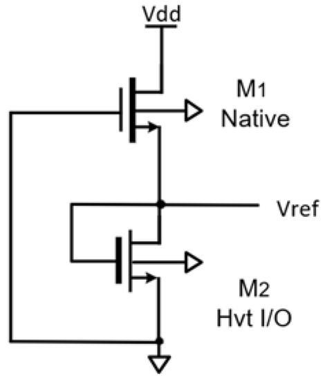
Figure 1.
Schematic of Conventional 2T Voltage Reference.
Referring to Figure 1, assume that all transistors work in the subthreshold region with > 4, and the respective drain-source current for and is approximated by
where is mobility, is oxide capacitance, is subthreshold factor ( = 1 + ) with denoted as depletion capacitance, is threshold voltage, and is thermal voltage ( = ). Since equals to , the reference voltage [18] is obtained as
When and are approximated as 1 [14], (3) can be approximated as follows
where and represent the subthreshold slope factor of and , respectively. Since has a negative T.C., it can be written as
is defined as the threshold voltage value at the reference temperature = 300 K, and is the absolute temperature coefficient of . Since displays negative T.C. while displays positive T.C., by selecting the proper width and length ratio for and , the temperature coefficient can be cancelled. The optimal transistor size that can be found to achieve zero TC is described as
By substituting (6) in (3), the temperature-compensated is written as
As particularly noted, from 49 dies, the best T.C. was 16.9 ppm/°C and the average T.C. was 62 ppm/°C, for the temperature range between −20 °C to 80 °C. Therefore, it is competitive for this type of voltage reference with respect to the conventional first-order compensated CMOS or BJT voltage references in the context of circuit simplicity and T.C. performance metric.
It can be found that the theoretical value of within zero-T.C. depends on the difference of value (Δ) between and . Therefore, the maximum is limited by the types of devices which are being employed. However, the circuit is difficult to support when a higher output reference voltage is required in the circuit design. In addition, line sensitivity depends on the relative output resistance contributed by the respective device, and . The native MOS device usually has poor output resistance when compared with that of IO device . Long channel design should often be utilized to relax the issue.
A self-regulated 3T voltage reference [15], as depicted in Figure 2, was proposed to improve the line sensitivity when the design was targeted in 65 nm CMOS technology. It is mainly because the resistance of the device is lower in the advanced technology node.
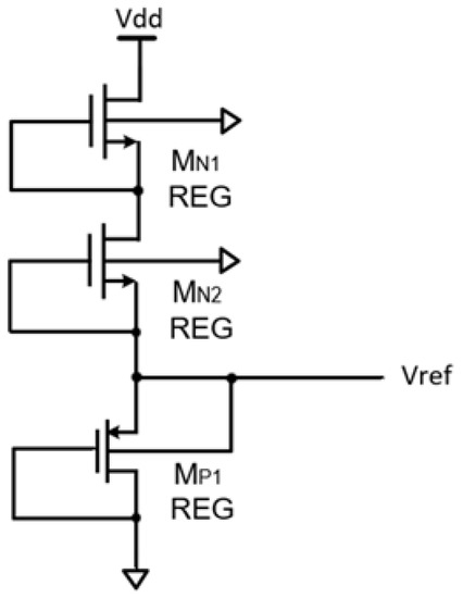
Figure 2.
Schematic of the 3T Self-regulation Voltage Reference.
The reported design involved the addition of a self-regulated transistor on top of the current generator NMOS device and the PMOS active load . As such, the equivalent impedance between the output node and the minimum supply voltage was increased while the parasitic capacitor coupling effect between them was reduced. Hence, the line sensitivity of 3T topology was improved by 3.7× when compared with that of the 2T topology in [14]. Despite the 3T topology utilizing high threshold and long channel length devices to attain fW level power consumption, the T.C. was degraded to 252.2 ppm/°C. However, the low output voltage had the same design concern as the 2T voltage reference.
Differing from the 3T voltage reference [15], a self-cascode current source and a self-cascode active load were employed to constitute a 4T voltage reference [16] as shown in Figure 3. The obtained T.C. was 81.9 ppm/°C from −40 °C to 140 °C, with 256 Monte Carlo samples.
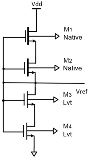
Figure 3.
Schematic of the 4T Voltage Reference.
Although the fluctuation of supply voltage was reduced, the 4T voltage reference was not able to produce a higher output voltage. As can be seen, the higher output value is merely achieved by increasing Δ between the current source and load transistors. Therefore, it is also often difficult to obtain high Δ value.
Other approaches based on the 2T based topology were proposed to yield a higher value of . The first design [14], as shown in Figure 4, made use of stacking two 2T voltage references to double the output voltage. It started with the first 2T voltage reference at the bottom level, the output of which was then used to drive the second 2T voltage reference in a cascade arrangement. The resulting output from the stacked topology would give a ×2 output voltage. The penalty paid for that was the degradation of T.C. performance due to the increase of circuit sensitivity.
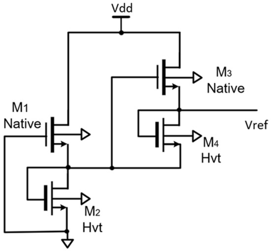
Figure 4.
Schematic of Stacked 2T Voltage References to Obtain Higher Output Voltage.
Alternatively, by employing the stacked PMOS transistors in the active load as depicted in Figure 5 [17], it was able to produce the scalable output voltage. Compared with the stacking 2T circuit [14], only one current source was used to pass the current through the series-connected PMOS diodes. As a result, it allowed both the chip area and the power consumption to be saved. Moreover, another key advantage of the topology was that the output voltage was governed by the number of added PMOS devices. There was a trade-off between the power consumption and T.C. due to the leakage current flowing through the parasitic diode formed by the n-well and p-substrate of PMOS devices. The higher the output voltage, the larger the tradeoff between circuit sensitivity and T.C. performance metric.
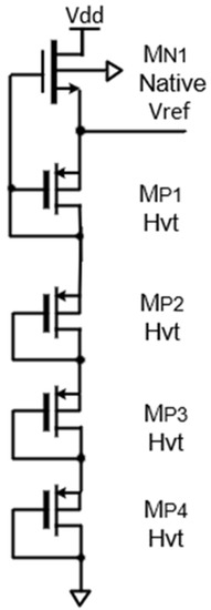
Figure 5.
Schematic of Voltage Reference with Scalable Output.
3. Modified 2T Voltage Reference with Output Voltage Doubling
The proposed voltage reference topology is depicted in Figure 6a. It is designed using 40 nm of CMOS process technology. The circuit comprises of a current source using a native NMOS transistor with negative and a diode-connected active load using a PMOS transistor with high , in conjunction with two identical resistors, and , as a resistive divider network to perform the voltage doubling function at the output of voltage reference. The reason to employ two identical resistors is to obtain the best matching characteristic. In addition, a non-dominant small current is designed to pass through the resistors so as to minimize the variation induced by resistors [19]. This can be achieved by means of a high resistance value. Unfortunately, the drawback of high resistance value is that of large chip size. Thus, the passive resistors, and , will be replaced by the identical diode-connected PMOS transistors, and , respectively. This gives the actual circuit as shown in Figure 6b. As particularly noted, the implementation of and , is based on high- PMOS transistors, taking advantage of lower mobility in p-type material. The resistive network permits the realization of a distributed RC filter by adding the capacitors, and , thus resulting in a sharp roll-off characteristic, which is particularly important for power supply rejection (PSR) at high frequencies.
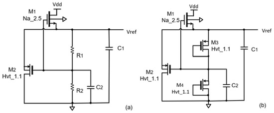
Figure 6.
(a) Schematic of Modified Voltage Reference with Resistive Divider for Output Voltage Doubling (b) Schematic of Modified Voltage Reference with Diode-connected PMOS Active Divider for Output Voltage Doubling.
For a NMOS transistor to operate in the subthreshold region, the drain-source current is expressed as
When > 4 , the term can be ignored. Hence, the drain-source current can be simplified in the form
Similarly, for a sub-threshold biased PMOS transistor, the source-drain current is expressed as
Since and are identical resistors, equals to 2 of . Then, the corresponding current flowing through the transistor , is given by
where and represent the subthreshold factor of and , respectively. and represent the effective aspect ratio of and , respectively. The current flowing through is the sum of the current passing through and the current passing through and , which is written as
where R represents the resistance value of and under identical design. The current relationship is obtained as
Using (11)–(14), the generated reference voltage is expressed as follows
where , which is the characteristic current for MOS transistor operating in subthreshold region. It can be observed that, when R is made as large as possible, the last term tends to be zero. Thus, when using large value resistors, (15) can be simplified as
As mentioned in Section 2, is a PTAT voltage, while Δ is a CTAT voltage [20]. Thus, we have
where and denote as and , respectively. It is the corresponding absolute value of temperature coefficient of threshold voltage for NMOS and PMOS device.
Thus, the rate of change of reference voltage with temperature can be obtained as
To achieve , the optimal aspect ratio for and to realize temperature compensation is given as
Substituting (20) in (16), the temperature-compensated is simplified in the form
Compared with (7) in the foundation 2T voltage reference, there is a multiplier of 2 in (21) from the proposed voltage reference. As a result of the sub-division method and identical design for resistors, and , in Figure 6a, indicates that the output voltage is doubled. In addition, and nearly equal to 1, thus it also reveals that the output voltage with temperature compensation is determined by the difference of reference threshold voltage and the difference of temperature coefficient of between and (. If and are made as large as possible, the highest output voltage value can be achieved. Here, PMOS with high is used for because of its high absolute value of threshold voltage in the process technology. In addition, a PMOS transistor also presents a relatively high temperature coefficient of threshold voltage when compared with that of a NMOS transistor. This is because the terms determining are (the metal-semiconductor work function potential difference) and (the associated band bending), which adds together in the PMOS transistor, instead of compensating each other for the NMOS transistor [21].
Moreover, higher output resistance of the current source benefits PSR. In the design, a large channel length is set for native ( = 22m) whereas a relatively smaller channel length ( = 3m) is utilized for high- . The choice of ’s channel length is to avoid the short-channel effect whilst providing good stability for transistor. For sustaining good PSR, the minimum approximated headroom of 200 mV is made for the of top transistor .
Concerning the large value of resistors and to achieve better T.C., the passive resistors are replaced by the diode-connected high- PMOS transistors, and . The dc resistance expressions for transistor and are obtained as follows:
From (22) and (23), the large resistance value is guaranteed by the small aspect ratio for each and in conjunction with the higher threshold voltages, and contributed by the high- PMOS devices.
The capacitors and and the active resistors, realized by and , serve as a distributed low-pass filter that provides a sharper roll-off characteristic. This significantly filters the high-frequency fluctuation from to the output through the devices. This improves the high-frequency PSR performance of the voltage reference. The sizes of devices in the design are listed in Table 1.

Table 1.
Sizes of Devices in the Proposed Design.
4. Results and Discussion
The proposed voltage reference is designed and implemented using TSMC 40 nm CMOS process technology. In order to compare different performance metrics of the 2T voltage reference [13] and its variants [14,15,16,17], the identical CMOS technology and similar level of current consumption is employed in each design. For filter capacitor used for PSR evaluation, identical capacitor size is adopted. In the comparative design, the supply current in each topology is set at about 5.5 nA, whereas the total capacitor size of each topology is 5 pF.
Refer to the modified topology in Figure 6b and other representative reported designs in Figure 7; all the component sizes and their responding values are listed in the corresponding Table 1 and Table 2.
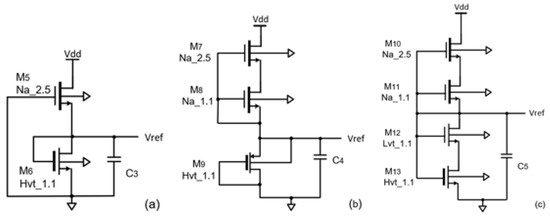
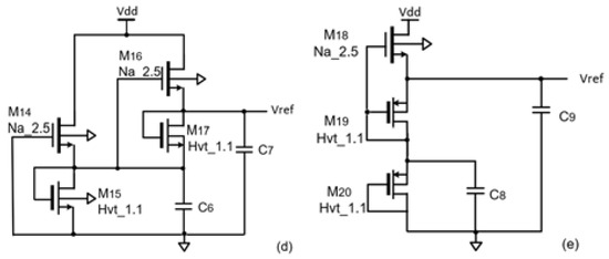
Figure 7.
Schematic of Voltage References in 40 nm Process Technology (a) 2T Design (b) 3T Design (c) 4T Design (d) Stacked 2T Design (e) Scalable Output Design.
Table 2.
Sizes of devices at different voltage reference designs in Figure 7.
Regarding the performance of modified 2T topology, the obtained T.C. from one sample simulation is 16.64 ppm/°C for the temperature range from −20 °C to 80 °C shown in Figure 8. This yields 0.815 mV variation at the nominal of 489.63 mV. Consider 200 samples of Monte-Carlo simulation results that comprises within-die (WID) variation and die-to-die (D2D) variation as depicted in Figure 9; the average T.C. of the proposed work is 29.6 ppm/°C and the standard deviation of T.C. is 13.26 ppm/°C. From the T.C. performance metric comparison, although the 2T and its stacked topologies offer lower standard derivation of T.C., with 8.19 ppm/°C and 9.1 ppm/°C, respectively, they display relatively higher values in average T.C., with 42.06 ppm/°C and 49.71 ppm/°C, respectively. For 3T and 4T circuits, the topologies suffer from an even higher average T.C., with corresponding 71.43 ppm/°C and 91.01 ppm/°C. The same goes for their standard derivation of T.C., with 41.79 ppm/°C and 53.45 ppm/°C, respectively. Finally, the scalable output topology offers 10.27 ppm/°C in the standard derivation of T.C. and 40.8 ppm/°C in the average T.C.
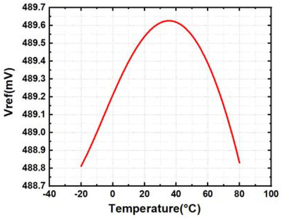
Figure 8.
against Temperature for 1 Sample.
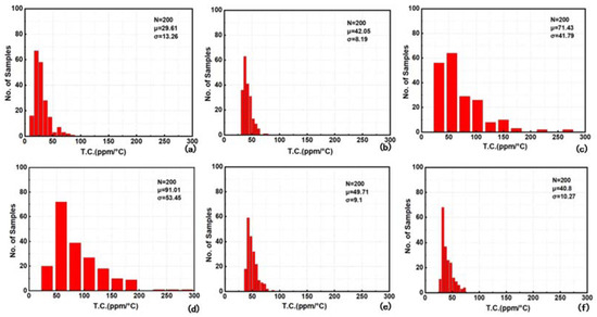
Figure 9.
Monte-Carlo Simulation of T.C. of (a) Modified 2T with Output Voltage Doubling Topology (b) 2T Topology (c) 3T Topology (d) 4T Topology (e) Stacked 2T Topology (f) Scalable Output Topology.
Through the comparison with those of prior-art topologies, it is suggested that proposed topology displays the best value for one-sample T.C. and the average T.C. under Monte-Carlo simulation with multiple samples. The standard derivation of T.C. is considered moderate and acceptable.
In order to evaluate the variation of among different topologies, the Monte-Carlo simulations are conducted for 200 samples, which take into account the WID variation and the D2D variation at a temperature of 27 °C, −20 °C and 80 °C in Figure 10, Figure 11 and Figure 12, respectively. Refer to the simulation results at a nominal temperature of 27 °C in Figure 10; the average of the proposed work is 488 mV. As can be observed, the obtained output voltage is higher than those of 2T, 3T and 4T, stacked 2T and scalable output circuits. The process sensitivity of the proposed work gives σ/μ = 3.9%. It is the lowest value with respect to those having 4.66%, 6.1%, 9.3%, 4.9% and 4.2% for 2T, 3T, 4T, stacked 2T and scalable output circuits, respectively. When operating at corner temperatures of 20 °C and 80 °C in Figure 11 and Figure 12, respectively, it can be observed that all the topologies have no significant change on the performance parameters. This has demonstrated that 2T based voltage references together with the variants are robust in nature. The stems from the topological simplicity in this category of voltage reference.
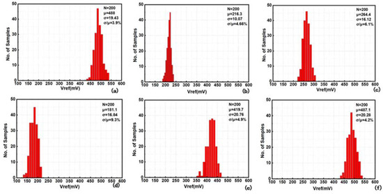
Figure 10.
Monte-Carlo Simulation of @27 °C (a) Modified 2T with Output Voltage Doubling Topology (b) 2T Topology (c) 3T Topology (d) 4T Topology (e) Stacked 2T Topology (f) Scalable Output Topology.
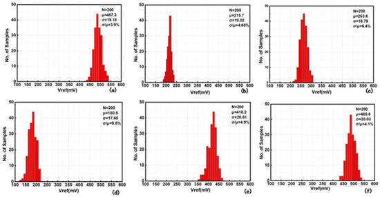
Figure 11.
Monte-Carlo Simulation of @−20 °C (a) Modified 2T with Output Voltage Doubling Topology (b) 2T Topology (c) 3T Topology (d) 4T Topology (e) Stacked 2T Topology (f) Scalable Output Topology.
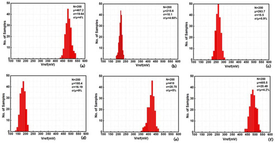
Figure 12.
Monte-Carlo Simulation of @80 °C (a) Modified 2T with Output Voltage Doubling Topology (b) 2T Topology (c) 3T Topology (d) 4T Topology (e) Stacked 2T Topology (f) Scalable Output Topology.
Figure 13 presents the PSR plot of the proposed work and its comparison with other topologies. As can be observed, the 3T and 4T circuits exhibit high lower frequency PSR values. This is due to the cascode arrangement for the top transistor. The rest of the other circuits, including the proposed work, offer medium values for low-frequency PSR. This is due to the finite device’s output resistance contributed by the 40 nm technology node. In this work, the obtained PSR is −45.5 dB at low frequency (100 kHz) and −76.3 dB at high frequency (100 MHz). The high frequency PSR is comparable with a majority of topologies. This is adequate for many analog circuit applications. Finally, all the simulation results pertaining to temperature of 27 °C, −20 °C and 80 °C are summarized and compared in Table 3, Table 4 and Table 5, respectively. The 2T circuit displays the lowest operation supply voltage among all the topologies, which is considered the key advantage. Regarding the proposed work, it has the disadvantage of a slight increase in minimum supply voltage, which is similar to the scalable output voltage topology. However, the proposed work offers the best 1-sample T.C., the best average T.C. under multiple samples, the highest output voltage as well as the maximum output voltage per minimum supply voltage. Additionally, it also gives low process sensitivity to because it keeps the property of simplicity similar to that of conventional 2T topology. Although the T.C. process sensitivity is in moderate value, it is still acceptable because low average T.C. is achieved in the proposed topology. The line sensitivity of the current work is reasonable. The slight degradation is due to the voltage headroom consumed by the PMOS diodes for the resistive divider. Nevertheless, the proposed work is a useful voltage reference block which offers balanced and comparable performance metrics.
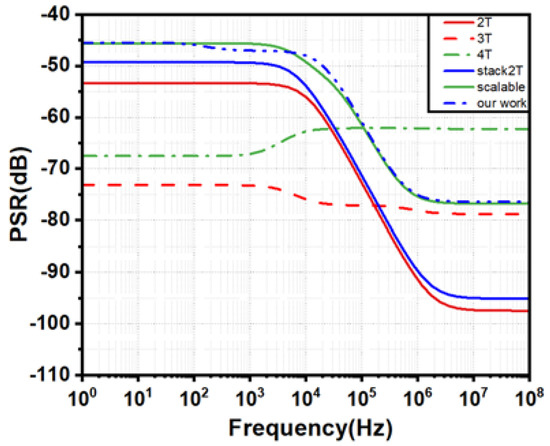
Figure 13.
PSR of the Proposed Voltage Reference and its Comparison with Other Designs.
Table 3.
Performance Comparison of the Simulation Results at 27 °C.
Table 4.
Performance Comparison of the Simulation Results at −20 °C.
Table 5.
Performance Comparison of the Simulation Results at 80 °C.
5. Conclusions
An improved voltage reference topology which is modified on the basis of the conventional 2T circuit is proposed in this work. Under the design at identical 40 nm CMOS technology and similar level of supply current consumption, the comparative simulation results have shown that the proposed circuit exhibits the best 1-sample T.C. and 200-sample average T.C. and the lowest process sensitivity with respect to that of the representative topologies such as 2T, 3T, 4T, stacked-2T and scalable output topologies. Additionally, the generated reference output voltage is also higher than 2T, 3T, 4T, stacked-2T and scalable output circuits, yielding maximum output voltage per minimum supply voltage. Finally, the proposed circuit provides balanced and comparable performance metrics in terms of line sensitivity and PSR. The voltage reference is very useful for the ultra-low power IoT applications.
Author Contributions
Conceptualization: J.L., P.K.C.; Validation: J.L. and P.K.C.; Writing: J.L.; Review and Editing: P.K.C. All authors have read and agreed to the published version of the manuscript.
Funding
This research received no external funding.
Institutional Review Board Statement
Not applicable.
Informed Consent Statement
Not applicable.
Data Availability Statement
Not applicable.
Conflicts of Interest
The authors declare no conflict of interest.
References
- Lim, J.; Lee, J.; Moon, E.; Barrow, M.; Atzeni, G.; Letner, J.G.; Costello, J.T.; Nason, S.R.; Patel, P.R.; Sun, Y.; et al. A Light-Tolerant Wireless Neural Recording IC for Motor Prediction with Near-Infrared-Based Power and Data Telemetry. IEEE J. Solid-State Circuits 2022, 57, 1061–1074. [Google Scholar] [CrossRef] [PubMed]
- Jeon, C.; Sim, J.-Y. A 2.5-NW Radio Platform With an Internal Wake-Up Receiver for Smart Contact Lens Using a Single Loop Antenna. IEEE J. Solid-State Circuits 2021, 56, 2668–2679. [Google Scholar] [CrossRef]
- Neshatvar, N.; Schormans, M.; Jiang, D.; Schmitt, S.; Detemple, P.; Demosthenous, A. An Implantable Phase Locked Loop MEMS-Based Readout System for Heart Transplantation. IEEE Trans. Circuits Syst. II Express Briefs 2022, 10, 4168–4172. [Google Scholar] [CrossRef]
- Kuijk, K.E. A Precision Reference Voltage Source. IEEE J. Solid-State Circuits 1973, 8, 222–226. [Google Scholar] [CrossRef]
- Banba, H.; Shiga, H.; Umezawa, A.; Miyaba, T.; Tanzawa, T.; Atsumi, S.; Sakui, K. A CMOS Bandgap Reference Circuit with Sub-1-V Operation. IEEE J. Solid-State Circuits 1999, 34, 670–674. [Google Scholar] [CrossRef]
- Leung, K.N.; Mok, P.K.T. A Sub-1-V 15-Ppm//Spl Deg/C CMOS Bandgap Voltage Reference without Requiring Low Threshold Voltage Device. IEEE J. Solid-State Circuits 2002, 37, 526–530. [Google Scholar] [CrossRef]
- Shrivastava, A.; Craig, K.; Roberts, N.E.; Wentzloff, D.D.; Calhoun, B.H. 5.4 A 32nW Bandgap Reference Voltage Operational from 0.5V Supply for Ultra-Low Power Systems. In Proceedings of the 2015 IEEE International Solid-State Circuits Conference-(ISSCC) Digest of Technical Papers, San Francisco, CA, USA, 22–26 February 2015; pp. 1–3. [Google Scholar]
- De Vita, G.; Iannaccone, G. An Ultra-Low-Power, Temperature Compensated Voltage Reference Generator. In Proceedings of the Proceedings of the IEEE 2005 Custom Integrated Circuits Conference, San Jose, CA, USA, 21–21 September 2005; pp. 751–754. [Google Scholar]
- De Vita, G.; Iannaccone, G.; Andreani, P. A 300 NW, 12 Ppm//Spl Deg/C Voltage Reference in a Digital 0.35 /Spl Mu/m CMOS Process. In Proceedings of the 2006 Symposium on VLSI Circuits, Honolulu, HI, USA, 15–17 June 2006; pp. 81–82. [Google Scholar]
- Magnelli, L.; Crupi, F.; Corsonello, P.; Pace, C.; Iannaccone, G. A 2.6 NW, 0.45 V Temperature-Compensated Subthreshold CMOS Voltage Reference. IEEE J. Solid-State Circuits 2011, 46, 465–474. [Google Scholar] [CrossRef]
- Yan, W.; Li, W.; Liu, R. Nanopower CMOS Sub-Bandgap Reference with 11 Ppm/°C Temperature Coefficient. Electron. Lett. 2009, 45, 627–629. [Google Scholar] [CrossRef]
- Ma, K.; Cao, Y.; Zhao, X. A Compact 65nm CMOS Sub-1-V All-MOSFET Voltage Reference with Low Average Temperature Coefficient of 13.9 ppm/°C. In Proceedings of the 2018 IEEE 61st International Midwest Symposium on Circuits and Systems (MWSCAS), Windsor, ON, Canada, 5–8 August 2018; pp. 186–189. [Google Scholar]
- Shihabudheen, T.; Babu, V.S.; Baiju, M.R. A Low Power Sub 1V 3.5-Ppm/°C Voltage Reference Featuring Subthreshold MOSFETs. In Proceedings of the 2008 15th IEEE International Conference on Electronics, Circuits and Systems, St. Julian’s, Malta, 31 August–3 September 2008; pp. 442–445. [Google Scholar]
- Seok, M.; Kim, G.; Blaauw, D.; Sylvester, D. A Portable 2-Transistor Picowatt Temperature-Compensated Voltage Reference Operating at 0.5 V. IEEE J. Solid-State Circuits 2012, 47, 2534–2545. [Google Scholar] [CrossRef]
- Wang, H.; Mercier, P.P. A 420 FW Self-Regulated 3T Voltage Reference Generator Achieving 0.47%/V Line Regulation from 0.4-to-1.2 V. In Proceedings of the ESSCIRC 2017—43rd IEEE European Solid State Circuits Conference, Leuven, Belgium, 11–14 September 2017; pp. 15–18. [Google Scholar]
- Gan, P.; Wu, Y.; Cao, Y.; Zhao, X. A Highly-Reliable and Energy-Efficient Physical Unclonable Function Based on 4T All-MOSFET Subthreshold Voltage Reference. In Proceedings of the 2019 Asian Hardware Oriented Security and Trust Symposium (AsianHOST), Xi’an, China, 16–17 December 2019; pp. 1–6. [Google Scholar]
- Lee, I.; Sylvester, D.; Blaauw, D. A Subthreshold Voltage Reference with Scalable Output Voltage for Low-Power IoT Systems. IEEE J. Solid-State Circuits 2017, 52, 1443–1449. [Google Scholar] [CrossRef]
- Alea, M.D.; Alarcon, L.P.; Hizon, J.R. A modified class of Seok ultra-low power voltage references for wireless sensor nodes. In Proceedings of the TENCON 2015—2015 IEEE Region 10 Conference, Macao, China, 1–4 November 2015; pp. 1–4. [Google Scholar]
- Norton, P.; Brandt, J. Temperature Coefficient of Resistance for P- and n-Type Silicon: P. Norton and J. Brandt. Solid-St. Microelectron. Reliab. 1978, 18, 411. [Google Scholar]
- Filanovsky, I.M.; Allam, A. Mutual Compensation of Mobility and Threshold Voltage Temperature Effects with Applications in CMOS Circuits. IEEE Trans. Circuits Syst. Part I Fundam. Theory Appl. 2001, 48, 876–884. [Google Scholar] [CrossRef]
- Klaassen, F.M.; Hes, W. On the Temperature Coefficient of the MOSFET Threshold Voltage. Solid State Electron. 1986, 29, 787–789. [Google Scholar] [CrossRef]
Publisher’s Note: MDPI stays neutral with regard to jurisdictional claims in published maps and institutional affiliations. |
© 2022 by the authors. Licensee MDPI, Basel, Switzerland. This article is an open access article distributed under the terms and conditions of the Creative Commons Attribution (CC BY) license (https://creativecommons.org/licenses/by/4.0/).