1. Introduction
The simple and well-known static inverter is the basis and starting design point of the several common CMOS digital logic gates [
1]. Despite its intrinsic simplicity and its wide usage in the digital domain, it is much more versatile than it looks and can be used in many analog applications, ranging from high-speed signal processing [
2,
3] under typical supply voltages to ultra-low voltage domain as seen within the analog–digital converter designs [
4,
5,
6,
7], and biomedical instrumentation amplifiers [
8]. The performance of such inverter-based dependent systems not only relies on their own topologies but is also dependent on the underlying Operational Transconductance Amplifiers (OTA) schematics [
9,
10,
11,
12,
13,
14,
15,
16]. If such a system’s basic analog blocks can be improved in any aspect, the whole system can benefit from it. Unfortunately, not all the performance characteristics can be improved simultaneously, as there are always trade-offs that must be considered and decided during the OTA design. In addition to that, a fair comparison between inverter-based OTA designs using the same CMOS technology is no longer easily found in the literature.
In this context, for the first time, this work presents a review of the existing basic single-stage inverter-based OTAs found in the current literature and compares their strengths and weaknesses for all circuits designed at the same PDK. The inverter-based topologies used here are the Nauta (N), Barthelemy (B), Vieru (V), and Mafredini (M) OTAs. Their main difference is the common-mode rejection techniques they employ, at which, in the end, there are trade-offs between their power consumption, area usage, complexity, and output voltage excursion. Furthermore, those can be mixed to make hybrid OTA topologies, which are proposed and presented here. The proposed hybrid OTA topologies are Barthelemy/Nauta (B/N), Barthelemy/Manfredini (B/M), Barthelemy/Manfredini (B/M), Manfredini/Vieru (M/V) OTAs. They are also designed with the same technology and compared with the basic single-stage ones.
The paper is organized as follows. Within
Section 2, the paper presents a CMOS inverter cell, its biasing circuit, and its optimal operation point for maximum linearity. Later, in
Section 3, the four basic inverter-based OTA topologies [
2,
3,
10,
11] are discussed. In
Section 4, five combinations of the previous OTA topologies, and how active frequency compensation [
17] can be used in the design of two-stage OTAs while improving common-mode rejection are presented.
Section 5 shows a fair comparison of each topology, using designs made with the same inverter cells, the same gain-bandwidth performance, and simulated with the same operating conditions. Finally,
Section 6 concludes this work.
2. CMOS Inverter
The CMOS inverter is the key building block used to create the OTAs proposed in this work. Consequently, the inverter-based OTAs performance characteristics, such as transconductance, gain-bandwidth, power consumption, common-mode rejection ratio (CMRR), and power-supply rejection ratio (PSRR), depends on the quality of the CMOS inverter design. Its properties, such as large and small-signal parameters, process variability, temperature, and supply voltage dependence, are thoroughly explained in [
18,
19].
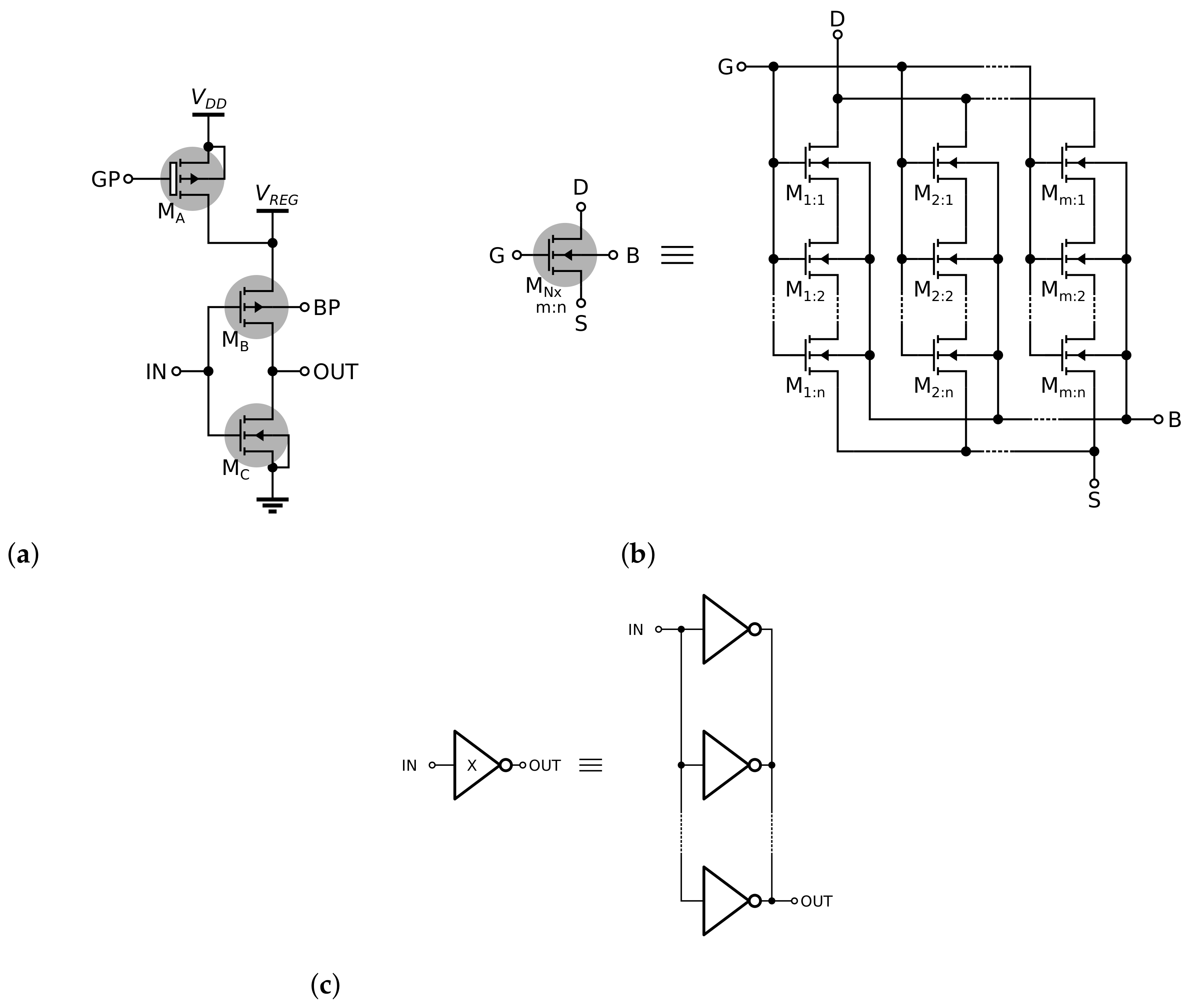
Figure 1a illustrates a custom CMOS inverter circuit diagram, which differs from the conventional CMOS inverter logic gate as it explicitly shows a dedicated driver transistor to control its supply voltage, and its PMOS transistor’s bulk terminal availability for body-biasing. Each transistor in this cell is, in fact, a rectangular transistor array [
20], made of a
m by
n matrix of single transistors, as shown in
Figure 1b. This inverter cell schematic, in particular, includes a third transistor and has two supplies: a higher supply voltage
and a regulated supply voltage
. Transistor M
A is made of thick oxide devices, and its function is to control
by properly biasing its gate voltage, which is connected to node GP. Transistors M
B and M
C compose the main CMOS inverter structure, and are made of thin oxide devices. Another custom modification is that the PMOS device bulk terminal is available for body-biasing, and it is connected to node BP, instead of
. Additionally, an inverter cell, as shown in
Figure 1c, is made of multiple cells in parallel with shared power supplies, input and output terminals, so its total small-signal transconductance
is a
X-folded the single inverter cell transconductance
.
A single inverter cell’s transconductance changes following Process, Supply Voltage, and Temperature (PVT) variations. For this reason, an OTA made of inverter cells must be biased by an external reference circuit, otherwise, the inverter-based OTA would suffer from large PVT variations jeopardizing the OTA functioning. An OTA’s transconductance can be tuned by varying its supply voltage [
2] or using body-biasing [
19,
21,
22,
23]. This work proposes a combination of both methods, using two different circuits.
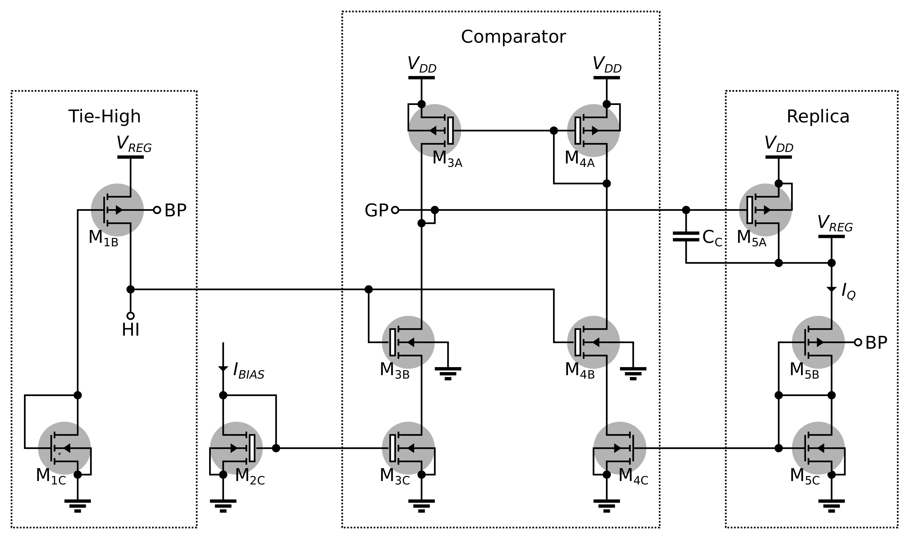
The first circuit, shown in
Figure 2, controls the OTA’s regulated supply voltage
; however, instead of setting
proportionally to a reference voltage, it is a function of a reference biasing current
. This circuit’s main goal is to make the replica inverter cell quiescent current
, also known as its short-circuit current, to follow the
. The circuit mirrors those currents, compares them, and controls the voltage at node GP, closing the negative feedback loop. This circuit considers that there is a supply voltage
higher than the desired
. Most commercial fabrication processes have thick and thin oxide devices available for different purposes in the same chip, rated for different maximum voltage drops. The proposed circuit has an additional circuit that prevents transistor M
4C’s drain-to-source voltage reaching voltages higher than
, using the protection think oxide transistor M
4B. To avoid connecting its gate terminal directly to
, and possibly incurring in antenna design rule violations, it is connected to node HI, from the tie-high circuit.
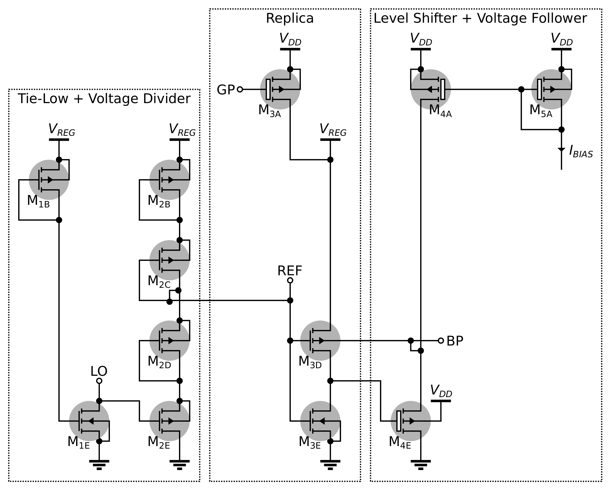
The second circuit is the quiescent voltage (also known as inverter trip-point or threshold voltage) biasing circuit, shown in
Figure 3. Its final goal is to set a fully differential inverter-based OTA’s output common-mode voltage to half supply, regardless of process variations [
19]. The REF node voltage is equal to half the regulated supply voltage
. Other body-bias circuits use resistor voltage dividers to achieve the same reference voltage [
10,
21,
24]; however, we are using diode-connected PMOS devices. Similar to the previous circuit, to avoid antenna design rule violations, transistor M
2E gate terminal is connected to the tie-lo output LO node, instead of being connected directly to the ground. Another difference from this circuit to the one proposed in [
19] is, since it has access to voltages higher than
, the PMOS devices can also be reverse-body-biased, which increases the body-biasing range. This happens because the voltage follower, made of the common-drain buffer stage, also works as a voltage level shifter.
As an example of the biasing circuit operation,
Figure 4a shows the resulting regulated supply voltage
as a function of the reference biasing current
for process corners TT, SS, and FF, for a constant supply voltage
at 5 V, and at room temperature. As expected, for the same
, different corners have different results. Nevertheless, as can be seen in
Figure 4b, an inverter cell biased this way, has almost identical transconductance curves as function of
, independently of the process corner.
The inverter quiescent voltage is a function of the supply voltage, the transistor model parameters, such as threshold voltage and charge mobility [
19], and transistor’s dimensions such as width (W) and length (L). For a typical process and operation conditions it should be designed to be close to the half voltage supply but without the expense of the inverter transconductance linearity, so the PMOS and NMOS contributions to the total transconductance would be as equal and symmetrical as possible. Since the PMOS device transconductance is relatively lower than the NMOS’ ones due to the inferior charge mobility of the holes compared to electrons, the PMOS transistor aspect ratio S = W/L must be larger. For this reason, all single inverter cells used in this work have PMOS transistors with aspect ratios about 3.33 times larger than their NMOS counterparts. Additionally, the PMOS devices are basically made of parallel transistor arrays while the NMOS are made of series transistor arrays, so their active areas are also similar. The inverter transistor dimensions is summarized in
Table 1.
Moreover, every CMOS inverter is sized to operate in the optimal operation condition for transconductance linearity [
22]. This behavior is depicted in
Figure 5a, which shows the inverter cell output current for a varying input voltage around the quiescent voltage, under a constant output voltage. As can be seen, the output current
has a different curvature for different supply voltages
, which directly affects the inverter transconductance, as shown in
Figure 5b. This effect is easier to observe by normalizing those the same curves as illustrated in
Figure 5c,d, respectively.
3. Basic Inverter-Based OTAs
The first inverter-based OTA was proposed by Nauta in 1989 [
2,
9].
Figure 6 shows its schematic. It is made of six inverters, has only four nodes, and is completely symmetrical. It is composed of two parts: the transconductor itself (inverters A) which is responsible for the OTA transconductance, and the common-mode rejection circuit, made of inverters B and C. This topology is essentially an attenuated positive feedback that works differently for differential and common-mode signals. Inverters C are cross-coupled and result in positive feedback for differential signals attenuated by inverters B, which are connected as loads. For common-mode signals, both inverters B and C are seen as loads by inverters A.
The small-signal low-frequency (DC) differential
and common-mode
voltage gains are functions of the inverters transconductances
and output conductances
Considering that the equivalent transconductance (output conductance)
of parallel inverter cells is proportional to the transconductance (output conductance) of a single inverter cell
and the inverter cell voltage small-signal voltage gain is equal to
, then for the special case where the inverter cell multipliers
,
Ideally,
should be designed to be slightly larger than
, so that we would have
and infinite differential voltage gain. To achieve this, inverters B and C could be designed with different sizes or biased independently [
2,
21]. However, as seen in
Figure 5b, the inverter transconductance is not linear and voltage gain would be only infinite for a point in the curve. Even if the inverter transconductances were perfectly linear, any variation due to PVT or local mismatch would decrease voltage gain or lead to hysteresis. For this reason, voltage gain improvement by this positive feedback technique is limited by a few dB, even using automatic biasing circuits [
24].
As an alternative to the Nauta OTA,
Figure 7a shows another inverter-based OTA based on the CM input feedforward rejection technique [
3]. This OTA topology main advantage is its output voltage headroom, as the Nauta topology greatly reduces it, even considering that the inverter cell output voltage headroom is almost rail-to-rail.
In this circuit, the common-mode input signal is extracted from the differential signals using inverters B and C. Then, this signal is fed forward to each output with inverted polarity, thus canceling the common-mode component of which is also amplified by inverter A, leaving the remaining input output differential signal. However, this common-mode cancelation is not perfect, as it is limited by the finite inverter voltage gain.
Applying the same reasoning was used for the Nauta OTA topology, for the special case, where
In this case, the common-mode voltage gain in the intermediate node is also unity. Other inverter multiplier ratios can be used but this one was selected so that it can have the same differential and common-mode voltage gain as the (N) OTA. Additionally, this OTA could be designed with for maximum power efficiency as it does not affect either and . However, this could lead to severe voltage offset problems due to transistor local mismatch.
A variant of Barthelemy OTA is the Vieru OTA as depicted in
Figure 7b. It is composed of the same number of cells and nodes, but the common-mode signal path direction is reverted so that the CM signal is fed back to the input. This topology is not advantageous alone, once it depends on the OTA input load. However, it can be useful as a cascaded two-stage OTAs [
10].
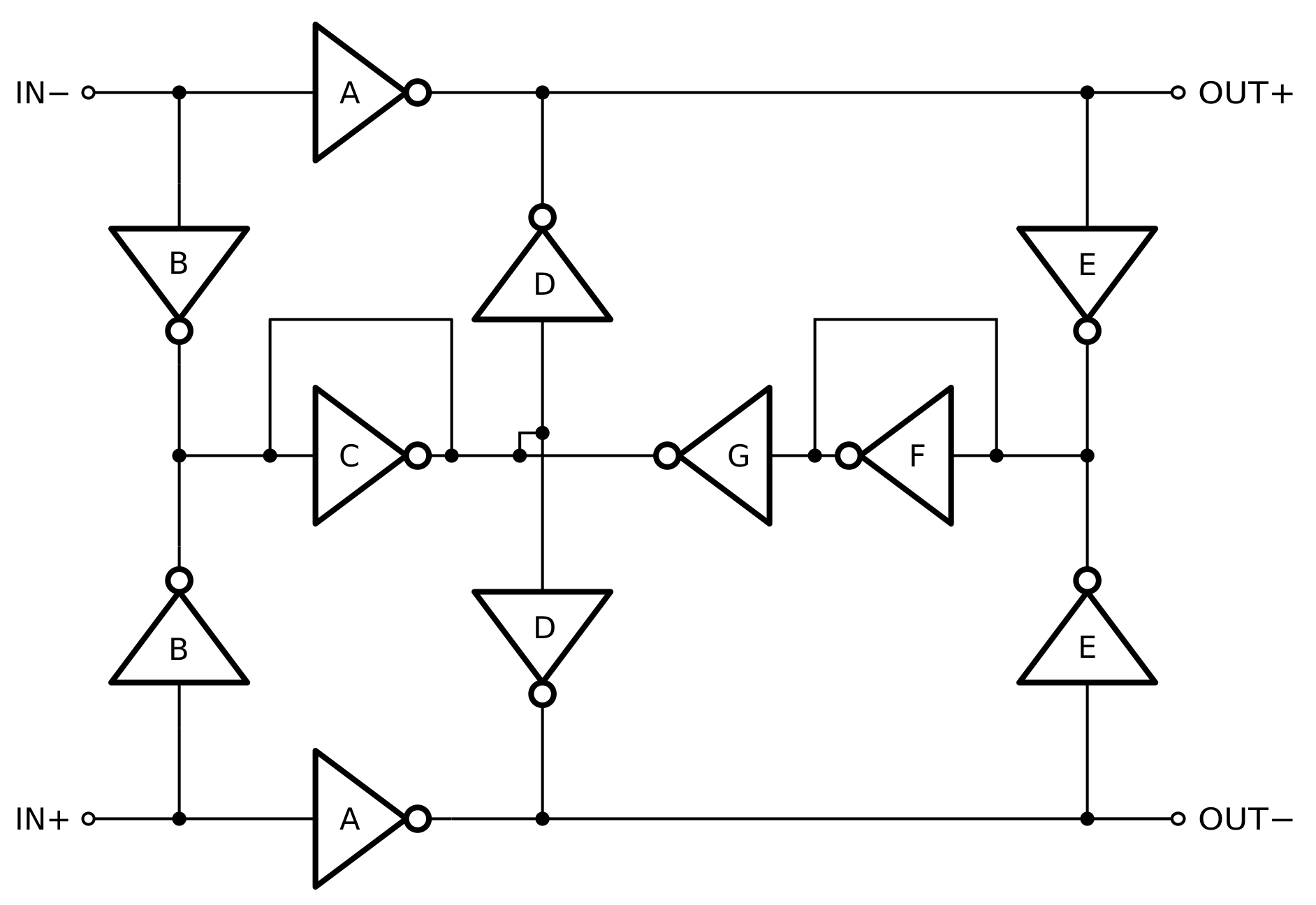
Another approach is to adopt a CM feedback technique which can be used in a standalone single-stage amplifier, as proposed in Mafredini [
11] by adding another node so that the output CM signal is fed back to the output nodes without going through the input nodes as done in the Vieru OTA topology.
Figure 8 shows the Manfredini OTA. As in the Nauta OTA the output signal is fed back to itself but without positive feedback. As in the Vieru OTA, the output common signal is extracted from the differential output signals by inverters B and C. Inverters D and E invert the common-mode signal polarity, and inverters F feed the common-mode signal back to the output canceling it. For differential signals, the circuit is ideally transparent. This common-mode technique is limited by the inverter cell low-frequency voltage gain, as shown in the small-signal analysis
For the special case where
,
the small-signal differential and common-mode voltage gains are similar to the previous topologies, once the common-mode path voltage gain is unity. Other inverter multipliers could be used to improve either the common-mode rejection or power efficiency, but this would result in the detriment of other OTA performance.
4. Proposed Hybrid Inverter-Based Amplifier Topologies
The previously presented OTA topologies can be merged to create hybrid versions. The OTA shown in
Figure 9 combines the common-mode feedforward and attenuated positive feedback techniques from Barthelemy and Nauta OTAs. The Barthelemy/Nauta (B/N) small-signal low-frequency voltage gains are
For the special case, where
and
As result, in this proposed B/N OTA, the common-mode voltage signal is further attenuated by a factor proportional to the inverter voltage gain. This is great for applications that need high common-mode rejection such as instrumental and biomedical signal amplifiers. However, B/N OTA suffers from the same drawback seen in the Nauta OTA; the output voltage excursion reduction.
A solution to keep the high common-mode rejection while having a reasonable output voltage signal headroom is to combine the Barthelemy and Manfredini (B/M) OTA topologies.
Figure 10 shows the second hybrid topology, which uses both CM input feedforward and output feedback techniques, by sharing the CM signal path to save area and power. Then, the B/M small-signal low-frequency voltage gains are
For the special case where
As seen in B/N, in B/M OTA the common-mode signal is attenuated by approximately the inverter voltage gain. This topology has the same number of intermediate nodes as the Manfredini OTA; however, it needs extra inverters, increasing this way its power consumption and the silicon area.
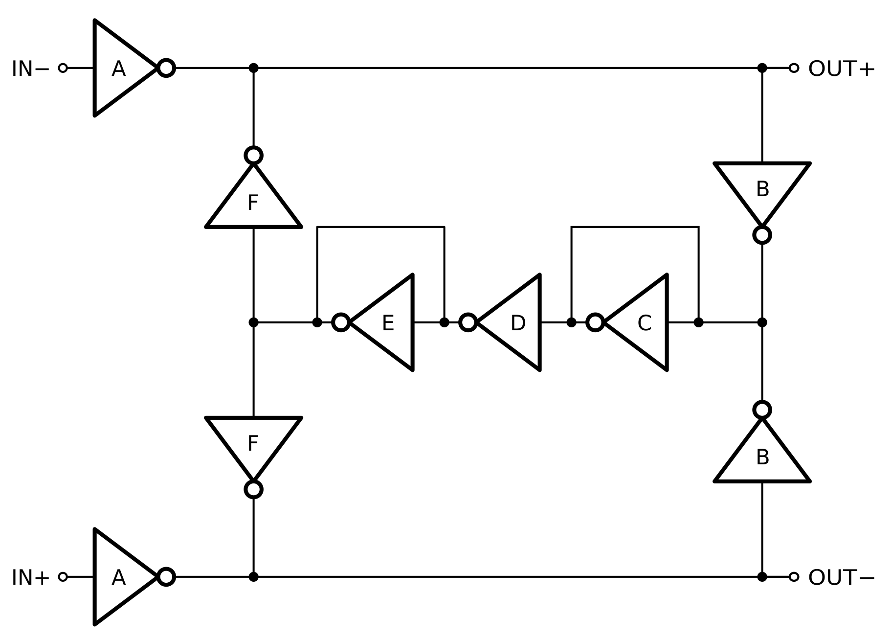
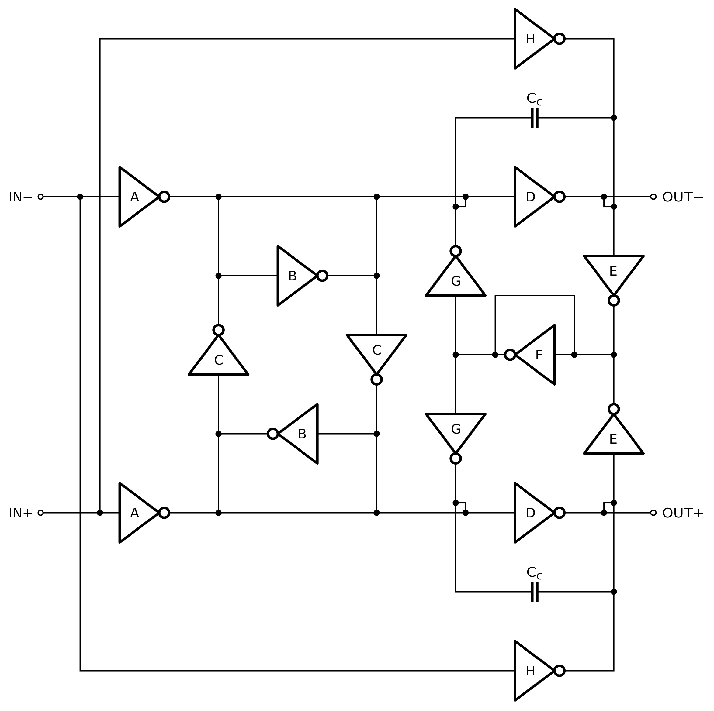
The basic and hybrid single-stage inverter-based OTAs seen so far are inherently stable once they do not have intermediate nodes in their differential signal path and there is no voltage gain in their common-mode signal path. Multi-stage amplifiers, on the other hand, need a frequency compensation circuit, if they are used within negative feedback networks. One of the simplest frequency compensation circuits is the Miller compensation capacitor, which implements the pole-splitting technique, which is normally followed by a zero-cancelation technique, mostly implemented with resistors. Another alternative is to use the so-called Nested Transconductance-Capacitance Compensation technique (NGCC) [
17], which is an approach that replaces the zero-canceling resistor with an active transconductance, and can be adapted to fully differential two-stage OTAs, as shown in
Figure 11.
Equation (
21) shows the open-loop transfer function for the number of stages
.
where
and
are the transconductance,
and
are the equivalent conductance of the first and second nodes across the Miller capacitor
, respectively.
Figure 12 depicts a two-stage amplifier [
6] comprised of two distinct Nauta stages with different strengths, and a Gm-C feedforward compensation path as described by Equation (
21) and in the
Figure 11. Given that all the design requirements to keep the circuit stable are considered according to Equation (
21), then the Nauta/Nauta (N/N) low-frequency small-signal gains are
and, for the special case where
,
, and
therefore, the differential voltage gain is proportional to two cascaded amplifiers, and the common-mode voltage gain is further attenuated as an effect of the feedforward path used for frequency compensation. However, the N/N OTA also suffers from the same degraded output voltage excursion of standalone N OTA.
Variants of N/N are also herein proposed considering the current advances in inverter-based OTA designs. Therefore, The N/N second stage can be replaced by the Vieru OTA from
Figure 7b, which implements output common-mode feedback to the inner nodes, as shown in
Figure 13. Considering the circuit is stable, the Nauta/Vieru (N/V) OTA have
as low-frequency gains for the differential and common-mode signals, respectively.
For
,
, and
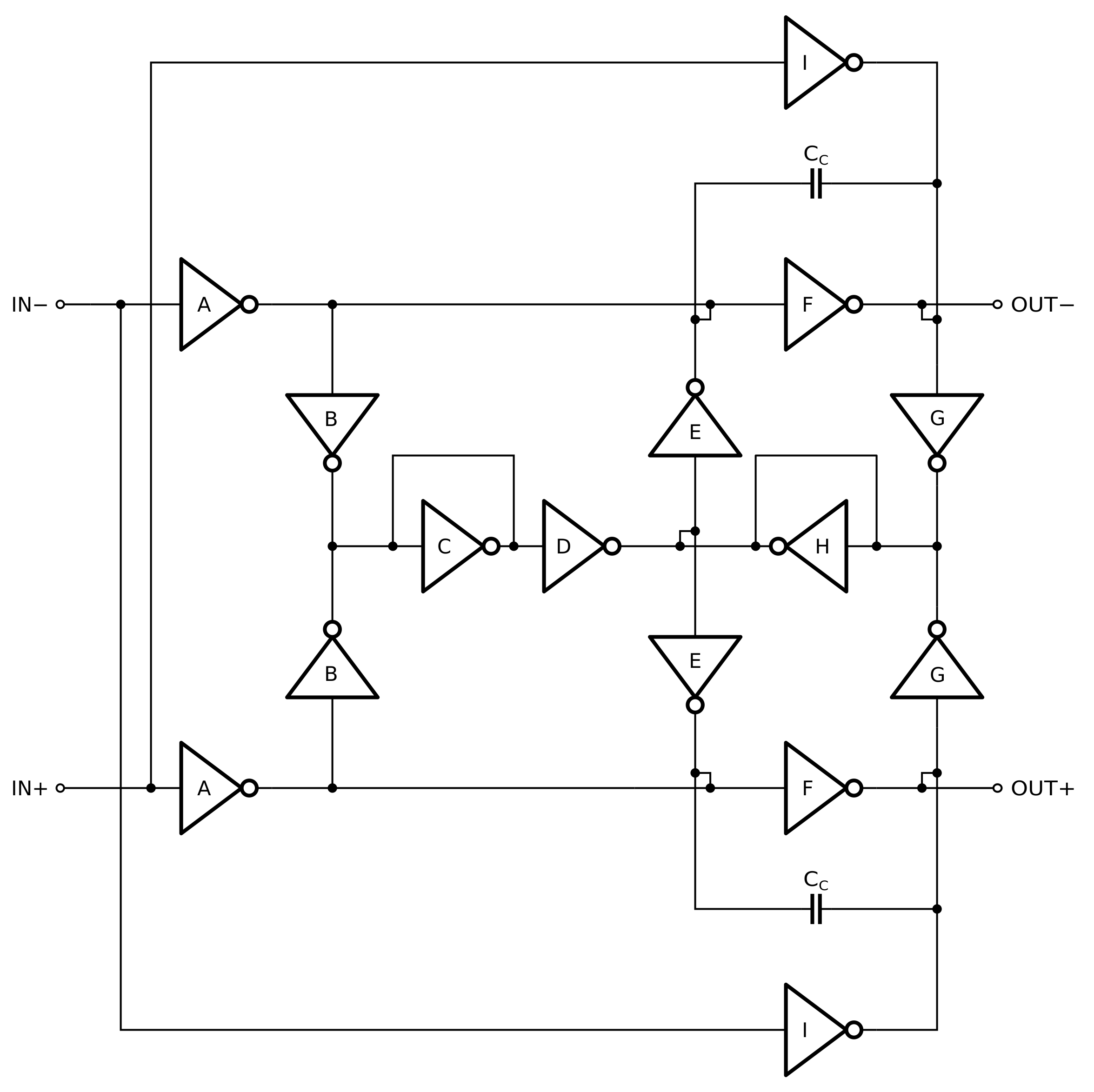
Another possibility is to further replace the first stage with a Manfredini stage of the
Figure 8, implement self-output common-mode feedback, and share the same path, as shown in
Figure 14. Making the same small-signal analysis and applying
,
,
and
, the Manfredini/Vieru (M/V) hybrid OTA has
as low-frequency gains for the differential and common-mode signals, respectively.
5. Simulation Results
All OTAs have been designed and simulated using Global Foundries 180 nm open-source PDK [
25] and open-source tools (ngspice simulator [
26] and Magic VLSI layout tool [
27]), and their spice netlists and results are available at [
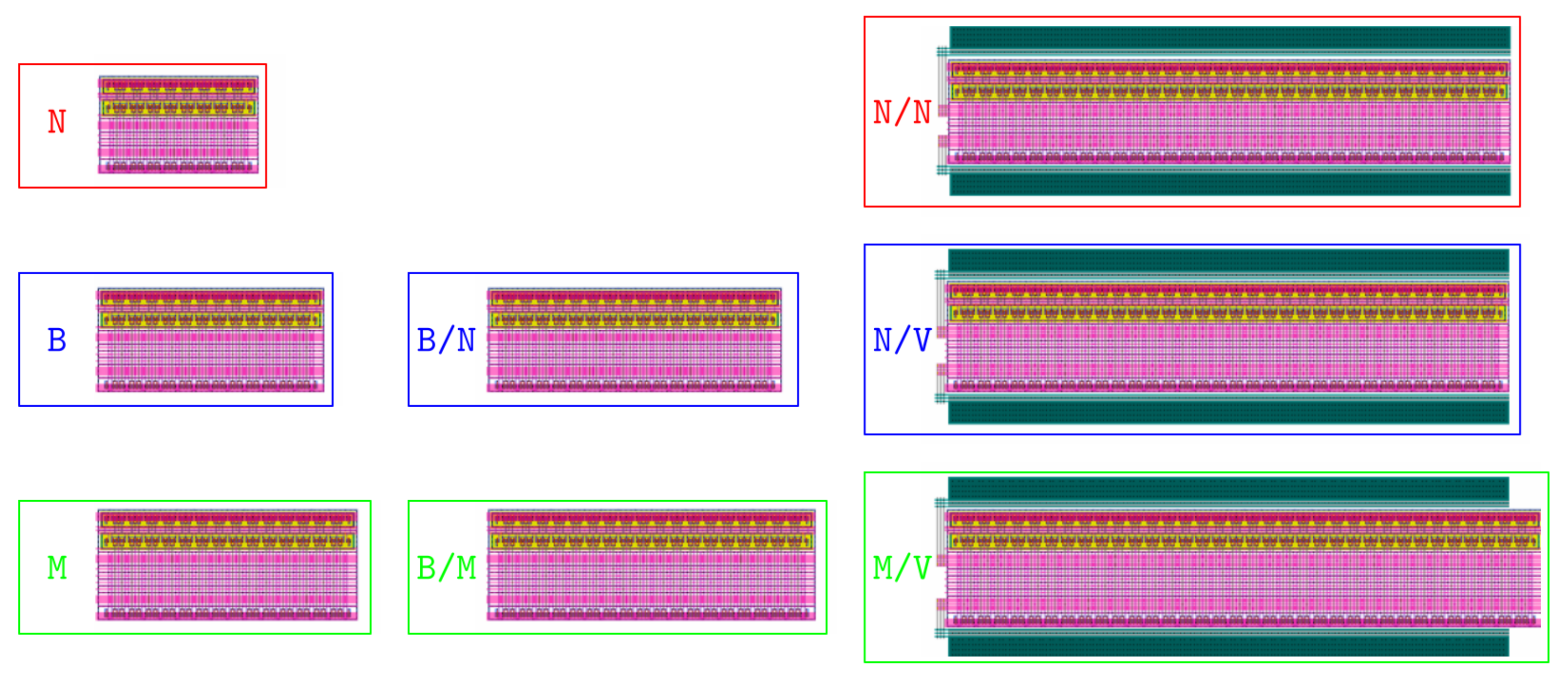
28]. All inverter cells are identical, and the number of parallel cells in each OTA individual inverter and total area is defined as in
Table 2. The OTA’s layouts are shown in
Figure 15.
5.1. Performance under Nominal Conditions
The post-layout simulations have used as parameters typical process corner, 3.0 V as supply voltage at room temperature and a 10 pF as capacitive load ().
As all single-stage OTAs have identical A inverters, they have almost identical differential AC output voltage gain (
), gain-bandwidth-product (GBW) and phase except for the B/N OTA, which has a slightly smaller low-frequency voltage gain, as shown in
Figure 16. The main difference is the common-mode voltage gain (
) as the B OTA has a shorter CMR bandwidth and both single-stage hybrid OTAs B/N and B/M OTAs have much lower CM voltage gain.
The small-signal power-supply common-mode voltage gain () at the output is negative, which implies that any fluctuation at the voltage supply is attenuated at the output. This is a direct result of the biasing circuit operation, as it works as a low dropout regulator, so the regulated supply voltage is tolerant to variations. Additionally, the hybrid OTA topologies have a slightly higher power-supply rejection than the basic ones.
The DC simulation results, depicted in
Figure 17, show the biggest difference between the basic Nauta, the Barthelemy, and Manfredini OTAs. As the N OTA has a lower output voltage swing, consequently, all hybrid OTAs which use this technique suffer from the same penalty. For this reason, the B/M hybrid OTA despite being larger and a bit more complex than the B/N hybrid OTA has a much larger output voltage swing while keeping a similar common-mode rejection.
Both Barthelemy and Manfredini OTAs have similar output voltage excursions however, they do not have rail-to-rail output, as it is limited by the transistor saturation region. This problem is solved using two-stage OTAs, as the first stage still contributes to voltage gain, even if the transistors connected to the output are operating in the low-gain linear region.
The two-stage OTAs have a much larger differential voltage gain and lower phase margin (PM), as expected. The feedforward frequency compensation technique also decreases common-mode voltage gain as a side-effect, so they have common-mode rejection results similar to the single-stage hybrid OTAs. Additionally, as the designs grow more complex and use more total transistors, not only their area, but their total current consumption () increases, so their power-efficiency Figure of Merit (FoM) decreases as well.
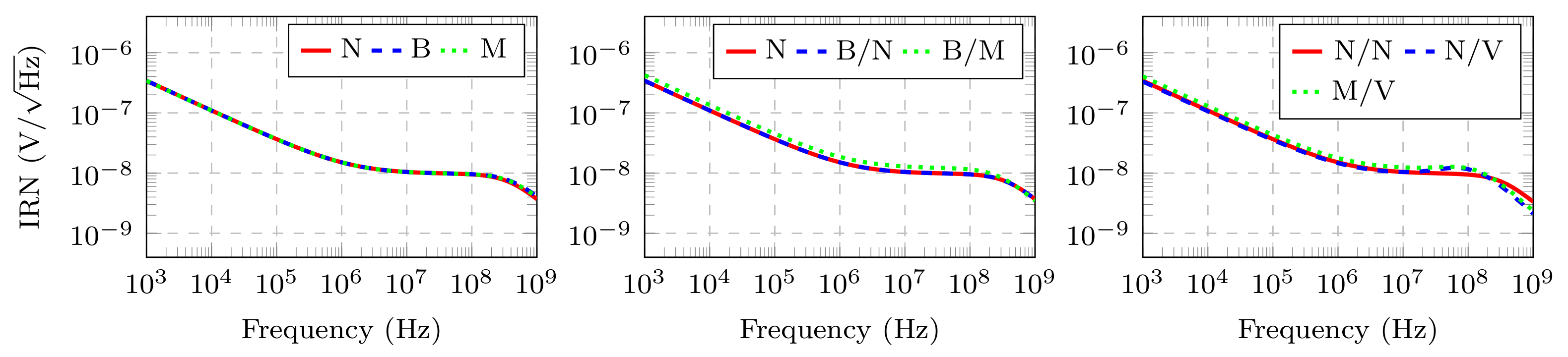
Figure 18 shows the noise simulation results. All OTAs have similar results, as they have the same number of inverter cells connected to their outputs, which results in the same voltage gain and transconductance. The two-stage OTAs also have similar results, as the first-stage output noise is dominant.
5.2. Process Variations and Monte Carlo Analysis
All OTAs have been simulated under process variations. For PVT corner simulations, the process corners TT, FF, and SS at 27, 70 and 0 °C were chosen and their results are summarized in
Table 3. As expected, since it is biased with an ideal current reference, current consumption variation is practically null, but the regulated supply voltage
varies accordingly, as a direct result of the biasing circuit operation. Voltage gain and GBW is slightly lower for higher temperatures as the OTA inverter transconductance must be decreasing with temperature for this operation point.
Monte Carlo simulations have also been run for every OTA, considering a 5 V supply voltage, and room temperature, for local mismatch only (Mis.), global mismatch only (Proc.), and both local and global mismatch enabled (All). A total of 100 runs were simulated for each case and its result summary is shown in
Table 4. As expected, there is an input voltage offset (
) resulting only from the local mismatch, and it is negligible for global mismatch, since the OTAs are symmetrical.
The output common-mode is calculated as the deviation from the expected value, which should be calculated as . Again, for global mismatch, all OTAs have similar results, as they are made of the same inverter cells and biased with the same circuit. However, for local mismatch, the Barthelemy OTA is an outlier, as its standard deviation is about 3.5 times larger than the others. As an absolute value, 36.5 mV is relatively small, considering a typical at 2.4 V. However, for ultra-low-voltage supplies at the range of a few hundred mV, this variation could be unacceptable.
The differential voltage gain variation is slightly larger for Nauta and its hybrid OTAs due to local mismatch, as there is positive feedback which can decrease or increase voltage gain. This effect can create outlier results, which can dramatically increase standard deviation, as seen in the Nauta/Nauta OTA.
6. Conclusions
Using 180 nm open-source PDK and open-source tools, this paper has described and compared in post-layout simulations, for the first time, the design of eight inverter-based OTAs: Nauta (N), Barthelemy (B), Mafredini (M), Barthelemy/Nauta (B/N), Barthelemy/Manfredini (B/M), Nauta/Nauta (N/N), Nauta/Vieru (N/V), and Manfredini/Vieru (M/V) OTAs. Based on simulation results without doubt the Nauta inverter-based OTA topology is the most power-efficient one, but its drawbacks are lower output swing. The other basic topologies, proposed by Barthelemy and Manfredini solve that by increasing the OTA complexity. Barthelemy and Manfredini OTAs have similar voltage excursions; however, the Barthelemy OTA output common voltage is intolerant to local mismatch, which should be a problem for lower supply voltages. Hybrid topologies merge those techniques and share paths, to save power and area while retaining the output swing of those alternative basic topologies. Using both Barthelemy and Nauta techniques increases the common-mode rejection; however, it also decreases the output voltage excursion, which is not a problem for the Barthelemy/Manfredini hybrid OTA. Single-stage inverter-based OTAs output voltage excursion does not include the supply voltages, but their multi-stage counterparts have rail-to-rail output voltage excursion. Finally, feedforward active frequency compensation makes two-stage amplifiers stable, and as a bonus, it can also improve common-mode rejection.


