Abstract
Graphene has attracted considerable interest as a prospective material for future electronics and opto-electronics. Here, the synthesis process of large area few layers graphene by Atmospheric Pressure Chemical Vapor Deposition (APCVD) technique is demonstrated. Quality assessments of graphene are performed and confirmed by Raman analysis and optical spectroscopy. Next, graphene was transferred on Polyethylene Terephthalate (PET) substrates and implemented as transparent conductive electrode in flexible Polymer Dispersed Liquid Crystal (PDLC) devices. Their electro-optical properties, such as voltage-dependent transmittance and flexibility behavior are measured and discussed. The stability of the sheet resistance after 1200 bending tests of graphene/PET structure is demonstrated. The obtained results open a great potential of graphene integration into the next generation Indium Tin Oxide (ITO) free flexible and stretchable optoelectronics.
1. Introduction
Graphene, an atomically thin two-dimensional material, is already proved to be very potential material for versatile applications in different areas of science and modern technologies. The enormous interest is motivated by the graphene’s distinctive properties as excellent optical transparency, ultra-high carrier mobility, elasticity, high mechanical strength, thermal and chemical stability, etc., which are successfully utilized in flexible and bendable optoelectronics, energy harvesting structures and biomedical sensors [1,2,3]. Moreover, graphene is regarded as the perfect optically transparent conductor to replace the currently widely used ITO [1]. Furthermore, graphene enables fabrication of curved surfaces and transformed shapes and shows high potential in flexible displays, foldable touch screens, paper-like displays, curved and flexible solid-state lighting devices and so on [4,5,6,7].
Among such extensively used methods to synthesize graphene as mechanical exfoliation, liquid-phase exfoliation, chemical synthesis and epitaxial growth on silicon carbide, the Chemical Vapor Deposition (CVD) technique has become the most popular and promising way for scalable graphene production [8,9,10,11,12,13,14]. Recent advances of CVD growth on metal substrates (Cu, Ni, Pt, Pd, Ir, Fe) led to the availability of large-scale and high-quality graphene, with controllable number of layers, limited defects and the best performance of graphene as transparent conductive films.
Typically, CVD processes involve two steps: the activation of gaseous reactants and a chemical reaction to form a stable solid deposit over the metal substrate. Generally, CVD can be divided into two types of process: (I) thermal assisted CVD and (II) plasma-enhanced CVD. The thermal CVD itself can be realized under low pressure (LPCVD) method or atmospheric pressure (APCVD) method commonly used for production of single, bi-layer or multilayer graphene. Although CVD growth of single layer graphene, due to its superior electrical transport properties, is highly anticipated despite being real challenging, the importance of multilayer graphene has rapidly grown because of its unique advantages for flexible optoelectronics providing ultra-flexible and transparent electrical contacts [11,12,13,14,15,16,17]. In this aspect, synthesis of multilayer graphene is important issue; moreover, it can provide superior electrical properties with the minor trade-off with optical transmittance reduction. For example, the roll-to-roll large area production [18] makes graphene a realistic candidate to be used in mass-produced flexible optoelectronic devices, organic and solid state solar cells, super capacitors, etc.
Recently, Polymer-Dispersed Liquid Crystals devices become very attractive for applications as outdoor displays, switchable privacy glasses, energy saving windows, light shutters, projection displays and so on [19,20]. In principle, PDLC are composite mixture of liquid crystal (LC) molecules randomly dispersed in a solid polymer matrix and due to the refractive index mismatch between the polymer matrix and the LC molecules. PDLC are naturally opaque (scatter the light at the initial state). PDLC can be switched from the light-scattering to the transparent state by application of an external electric field, which support the refractive indices match between the LC molecules and the polymer, and this functionality determines the unique behavior of PDLC devices.
In this study, the optical and electrical properties of multilayer graphene grown by APCVD were determined and the application of graphene films as transparent electrodes in flexible PDLC devices have been addressed.
2. Experimental
In this work, graphene was synthesized by APCVD method using copper foil (Alfa Aesar 99.8% purity, 25 µm thickness) in a set up shown in Figure 1a. A preliminary surface cleaning of the Cu foil was performed by sonication in acetone and propanol followed by deionized (DI) water rinsing and dry blowing with nitrogen. Before loading into the CVD tube reactor, the Cu foil was treated with acetic acid to remove the superficial copper oxide. First, the Cu foil was annealed at 1030 °C for 30 min in argon (Ar) and hydrogen (H2) atmosphere. After that, CH4 gas flow was introduced and the growing process continue in the gas mixture ratio of Ar:H2:CH4 = 450:50:10 cm3/min. The CH4 served as a carbon feedstock gas and was used only during the growth process. Finally, when the growth process completed the reactor tube was rapidly cooled to room temperature with a speed of 50 °C/min (Figure 1b). By following the above procedure continuous large area of graphene on Cu foil surface was synthesized.
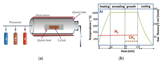
Figure 1.
(a) APCVD experimental set-up and (b) temperature/time diagram of growing multilayer graphene.
The graphene film was transferred on 100 micrometer thick PET substrates by spin coating of poly(methyl-methacrylate) PMMA (4% in anisole) on the top of graphene/Cu sheets. The PMMA/graphene/Cu foil was floated on Fe (NO3)3·9H2O solution to etch the Cu foil. The resultant film with PMMA and graphene was transferred to PET substrates, followed by removal of the PMMA by using substrates heating at 80 °C in acetone.
Raman spectroscopy was used to analyze the quality of the graphene layers and confirming multi-layer graphene structure. The Raman equipment consists of a 488 nm DPSS laser, spectrometer (HORIBA, Lab RAM HR) and CCD. An objective lens (100×, N.A = 0.9) was used to focus the laser with a resolution of ~1 μm at the laser intensity at 10 mW.
The optical transmittance spectrum of graphene/PET was measured at room temperature using an Ultraviolet-Visible-Near-infrared (UV-VIS-NIR) spectrophotometer Shimadzu UV–3600. The same measurement was performed on PET substrate for comparison.
The sheet resistance was measured using a four-point probe technique on an Ossila apparatus. Computerized home-built bending setup with an ESP301 control platform to stimulate bending at different radius was used for bending test of the graphene/PET samples. The sheet resistance of the samples was measured in the interval of up to 1200 bending cycles.
Based on the above characteristics, several graphene/PET substrates have been selected for PDLC devices fabrication. First, empty cells were assembled by composing graphene/PET substrates with the graphene layer facing each to other, separated with Mylar spacer (12 μm) in order to keep the uniform thickness. Then, PDLC mixture was made using UV-curable monomer NOA65 and E7 nematic liquid crystal at 30:70 wt.% ratio. Next, the LC/monomer mixture was injected into an empty cell and exposed with ultraviolet light (λ = 365 nm) for 15 min to polymerize NOA65. As a result of a phase separation, formation of randomly dispersed LC droplets in a polymer matrix appears.
The electro-optical characteristics of graphene/PET supported PDLC devices were measured by using a He-Ne laser as light source and applied alternating current (AC) voltage at 1 kHz frequency.
3. Results and Discussions
Figure 2a shows the Raman spectrum of graphene grown on Cu foil, characterized with very strong G-peak, located at ~1582 cm−1 and 2D-peak, located at ~2718 cm−1 with an intensity ratio I(2D)/I(G) of ~0.474. The D-peak (located at 1350 cm−1), which is a result of the defects and inhomogeneity in the sample, has moderate intensity, indicating the formation of good quality multilayer (4 to 5 layers) graphene [21].
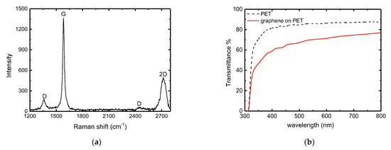
Figure 2.
(a) Raman spectrum of graphene grown on Cu foil and (b) Optical transmittance spectra of graphene on PET and PET substrate at UV-VIS spectral range.
The optical transmittance spectrum of graphene/PET at visible and near infrared spectral range is shown at Figure 2b. A comparison with the transmittance of blank PET is also presented for reference.
The sheet resistance dependence on the number of bending cycles was tested by using home-built bending setup shown at Figure 3. Multilayer graphene demonstrates excellent bending ability for more than 1200 times of cycling as shown in Figure 3c. Hence, by controlling the number of graphene layers, optical and electrical properties can meet the up-to-date standard requirements for ITO-free optoelectronics with acceptable sheet resistance and optical transparency values [22].
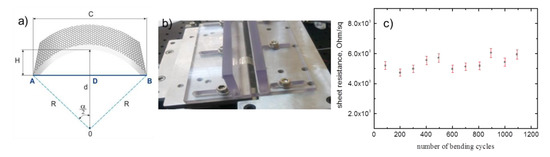
Figure 3.
(a) Schematic diagram for bending radius (R) calculation, (b) part of bending test set-up and (c) sheet resistance dependence of the number of bending cycles at 2.5 mm bending radius.
The remarkable sheet resistance stability under bending of graphene opens many opportunities for applications in flexible, stretchable and bendable optoelectronics.
Based on the above performed characteristics, an application of multilayer graphene on PET as transparent conductive layer in flexible PDLC devices is demonstrated.
Figure 4a shows the schematic structure of PDLC device using the graphene films as electrodes. The transmittance behavior was monitored as a function of applied voltage and it is shown at Figure 4b. We measured the threshold voltage Vth (defined as an applied voltage value to reach 10% of the maximum transmittance T10) for turning on the PDLC device of ~20 V and saturation voltage Vsat (defined as a value of applied voltage to reach 90% of maximum transmittance T) of ~70 V. As a result, by the application of an appropriate electric field the intensity of the transmitted light throughout the structure can be controlled.
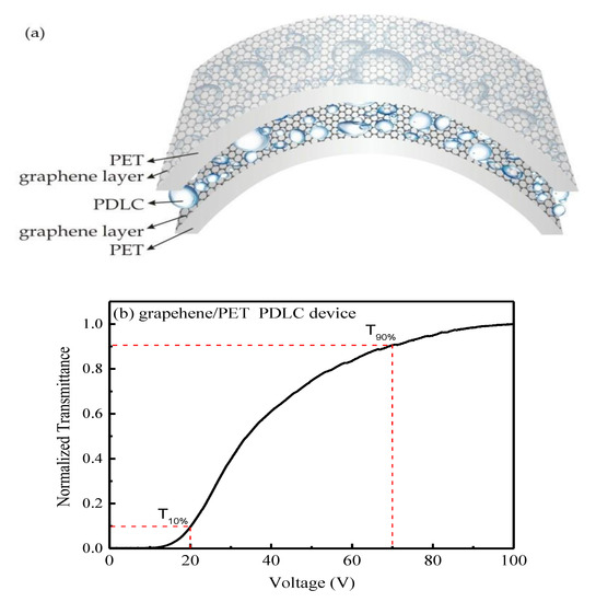
Figure 4.
(a) Schematic structure of PDLC flexible device (b) Voltage-transmittance characteristics demonstrating “on” and “off” states of the device.
4. Conclusions
This work demonstrates the growth, characterizations and applications of multilayer graphene as transparent conductive electrode for flexible display devices. Multilayer graphene was synthesized using the Chemical Vapor Deposition technique and its optical and electro-optic characteristics were measured. Multilayer graphene on a flexible PET substrate demonstrates excellent bending ability with almost constant sheet resistance values over 1200 times of bending. The demonstration of flexible PDLC device opens a great potential of graphene integration into the next generation flexible and stretchable ITO-free optoelectronics.
Supplementary Materials
The following are available online at https://www.mdpi.com/article/10.3390/IOCN2020-07900/s1.
Author Contributions
Conceptualization, V.M., D.D., K.-Y.H. and S.-H.L.; methodology V.M., S.P., D.P., D.D. and S.Y.L.; software S.P., B.N. and Y.M.; formal analysis, S.P., B.N., Y.M. and D.P.; resources V.M., D.D. and S.-H.L.; writing—original draft preparation, V.M., D.P., D.D. and S.-H.L.; writing—review and editing V.M., D.P., D.D., K.-Y.H. and S.-H.L.; visualization, V.M., S.P., B.N., J.M., D.P., D.D. and S.-H.L.; supervision V.M., D.P., D.D., K.-Y.H. and S.-H.L.; funding acquisition V.M., D.D. and S.-H.L. All authors have read and agreed to the published version of the manuscript.
Funding
This work is supported by the Bulgarian National Science Fund project # DFNI КП-06-H-28/8 and Ministry of Science and Technology (MOST), Taiwan under the contract’s numbers MOST 107-2221-E-009-120-MY3 and MOST 109-2927-I-009-507 (Bulgaria -Taiwan PPP project). We are also grateful for the support from the Higher Education Sprout Project of the National Chiao Tung University and Ministry of Education (MOE), Taiwan. Research equipment of Distributed Research Infrastructure INFRAMAT, part of Bulgarian National Roadmap for Research Infrastructures, supported by Bulgarian Ministry of Education and Science was used in this investigation.
Institutional Review Board Statement
Not applicable.
Informed Consent Statement
Not applicable.
Data Availability Statement
Data sharing is not applicable to this article.
Conflicts of Interest
The authors declare no conflict of interest.
References
- Woo, Y.S. Transparent Conductive Electrodes Based on Graphene-Related Materials. Micromachines 2019, 10, 13. [Google Scholar] [CrossRef] [PubMed]
- Zheng, Q.; Kim, J.K. Graphene for Transparent Conductors Synthesis, Properties and Applications; Springer: Berlin/Heidelberg, Germany, 2015. [Google Scholar]
- Xu, Y.; Liu, J. Graphene as Transparent Electrodes: Fabrication and New Emerging Applications. Small 2016, 12, 1400–1419. [Google Scholar] [CrossRef] [PubMed]
- Polat, E.O.; Balci, O.; Kakenov, N.; Uzlu, H.B.; Kocabas, C.; Dahiya, R. Synthesis of large area graphene for high performance in flexible optoelectronic devices. Sci. Rep. 2015, 5, 16744. [Google Scholar] [CrossRef] [PubMed]
- Akinwande, D.; Huyghebaert, C.; Wang, C.H.; Serna, M.I.; Goossens, S.; Li, L.J.; Wong, H.S.P.; Koppens, F.H.L. Graphene and two-dimensional materials for silicon technology. Nature 2019, 573, 508–518. [Google Scholar] [CrossRef] [PubMed]
- Randviir, E.P.; Brownson, D.A.C.; Banks, C.E. A decade of graphene research: Production, applications and outlook. Mater. Today 2014, 17, 426–432. [Google Scholar] [CrossRef]
- Marinova, V.; Lin, S.H.; Petrov, S.; Chen, M.S.; Lin, Y.H.; Hsu, K.Y. Graphene-based spatial light modulator operating at near infrared spectral range. Appl. Surf. Sci. 2019, 472, 2–9. [Google Scholar] [CrossRef]
- Wang, C.; Vinodgopal, K.; Dai, G.P. Large-Area Synthesis and Growth Mechanism of Graphene by Chemical Vapor Deposition. Chem. Vap. Depos. Nanotechnol. 2018, 5, 97–113. [Google Scholar]
- Arco, L.G.; Zhang, Y.; Kumar, A.; Zhou, C. Synthesis, Transfer, and Devices of Single- and Few-Layer Graphene by Chemical Vapor Deposition. IEEE Trans. Nanotechnol. 2009, 8, 135–138. [Google Scholar] [CrossRef]
- Yao, Y.; Li, Z.; Lin, Z.; Moon, K.-S.; Agar, J.; Wong, C. Controlled Growth of Multilayer, Few-Layer, and Single-Layer Graphene on Metal Substrates. J. Phys. Chem. 2011, C 115, 5232–5238. [Google Scholar] [CrossRef]
- Muñoz, R.; Gómez-Aleixandre, C. Review of CVD Synthesis of Graphene. Chem. Vap. Depos. 2013, 19, 297–322. [Google Scholar] [CrossRef]
- Kasap, S.; Khaksaran, H.; Çelik, S.; Ozkaya, H.; Ismet, C.Y.; Kay, I. Controlled growth of large area multilayer graphene on copper by chemical vapour deposition. Phys. Chem. Chem. Phys. 2015, 17, 23081–23087. [Google Scholar] [CrossRef] [PubMed]
- Ullah, Z.; Riaz, S.; Li, Q.; Atiq, S.; Saleem, M.; Azhar, M.; Naseem, S.; Liu, L. A comparative study of graphene growth by APCVD, LPCVD and PECVD. Mater. Res. Express 2018, 5, 035606. [Google Scholar] [CrossRef]
- Lai, Y.C.; Yu, S.C.; Rafailov, P.M.; Vlaikova, E.; Valkov, S.; Petrov, S.; Koprinarova, J.; Terziyska, P.; Marinova, V.; Lin, S.H.; et al. Chemical vapour deposition growth of graphene layers on metal substrates. J. Phys. 2016, 558, 01205. [Google Scholar] [CrossRef]
- Lai, Y.C.; Rafailov, P.M.; Vlaikova, E.; Marinova, V.; Lin, S.H.; Yu, P.; Chi, G.C.; Dimitrov, D.; Sveshtarov, P.; Mehandjiev, V.; et al. Chemical vapour deposition growth and Raman characterization of graphene layers and carbon nanotubes. J. Phys. 2016, 682, 012009. [Google Scholar] [CrossRef]
- Petrov, S.; Rafailov, P.M.; Marinova, V.; Lin, S.H.; Lai, Y.C.; Yu, P.; Chi, G.C.; Dimitrov, D.Z.; Karashanova, D.; Gospodinov, M. Chemical vapor deposition growth of bilayer graphene via altering gas flux geometry. Thin Solid Films 2019, 60, 137521. [Google Scholar] [CrossRef]
- Pham, P.V. Atmospheric Pressure Chemical Vapor Deposition of Graphene. Chem. Vap. Depos. Nanotechnol. 2018, 6, 115–134. [Google Scholar]
- Bae, S.; Kim, H.; Lee, Y.; Xu, X.; Park, J.-S.; Zheng, Y.; Balakrishnan, J.; Lei, T.; Kim, H.R.; Song, Y.I.; et al. Roll-to-roll production of 30-inch graphene films for transparent electrodes. Nat. Nanotechnol. 2010, 5, 574–578. [Google Scholar] [CrossRef]
- Coates, D. Polymer-dispersed liquid crystals. J. Mater. Chem. 1995, 5, 2063–2072. [Google Scholar] [CrossRef]
- Ahmad, F.; Jeon, Y.J.; Jamil, M. Graphene-based polymer dispersed liquid crystals display—An overview. J. Mol. Cryst. Liq. Cryst. 2018, 669, 46–60. [Google Scholar] [CrossRef]
- Ferrari, C.; Meyer, J.C.; Scardaci, V.; Asiraghi, C.C.; Lazzeri, M.; Mauri, F.; Piscanec, S.; Diang, J.; Novoselov, K.S.; Roth, S.; et al. Raman Spectrum of Graphene and Graphene Layers. Phys. Rev. Lett. 2007, 97, 187401. [Google Scholar] [CrossRef]
- De, S.; Coleman, J.N. Are There Fundamental Limitations on the Sheet Resistance and Transmittance of Thin Graphene Films. Nano Lett. 2009, 9, 4359–4363. [Google Scholar] [CrossRef] [PubMed]
Publisher’s Note: MDPI stays neutral with regard to jurisdictional claims in published maps and institutional affiliations. |
© 2020 by the authors. Licensee MDPI, Basel, Switzerland. This article is an open access article distributed under the terms and conditions of the Creative Commons Attribution (CC BY) license (https://creativecommons.org/licenses/by/4.0/).