Abstract
We report the characterization of back-gated field-effect transistors fabricated using platinum diselenide () ultrathin films as a channel. We perform a detailed study of the electrical conduction as well as of the photoconductivity. From the gate modulation of the channel current, we obtain the signature of p-type semiconducting conduction with carrier mobility of about 30 cm2 V−1 s−1. More interestingly, devices exposed to light, either in air and in vacuum, exhibit negative photoconductivity, which we explain by a photogating effect due to charge trapping in the gate dielectric and light-induced desorption of adsorbates.
1. Introduction
Two-dimensional (2D) transition-metal dichalcogenides (TMDs) have been widely investigated for their interesting properties and applications [1,2,3,4]. More recently, TMDs based on group-10 transition metals such as ad have attracted growing attention [5,6,7]. These materials crystallize in an octahedral lattice structure where the transition metal atoms are coordinated with six chalcogens. The presence of d-electrons in the group-10 transition metals gives rise to additional semiconductor bands making the electrical and optical properties largely tunable by the number of layers [8]. Monolayer has an indirect bandgap of ~1.2 eV, which is expected to reduce to 0.3 eV for the bilayer and vanish for the bulk [9].
The bandgap of covers the spectral range that is important for telecommunications and solar energy harvesting [10], and the carrier mobility (theoretically predicted up to 4000 [11] and experimentally found to be around [12]), competitive with black phosphorus, can enable fast electronic devices [13].
In this paper, we study the electrical properties of field-effect transistor realized using 3 nm-thick film. We report semiconducting p-type conduction, and relatively high hole mobility.
Interestingly, we report photoconduction measurements that demonstrate that the devices show negative photoconductivity, which we explain by a photogating effect due to charge trapping in the gate dielectric and light-induced desorption of adsorbates.
2. Experimental Section
film, obtained by direct selenization of 0.7 nm thick Pt film (fabrication details in ref. [14]), is transferred on /p-Si substrate and it is etched by SF6-based inductively coupled plasma process. The patterned (6 layers thick) is then contacted by Ni(20 nm)/Au(150 nm) metal leads. A schematic of the FET is shown in Figure 1a.
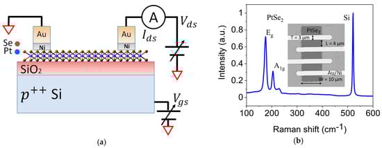
Figure 1.
(a) Schematic of back-gated FET and measurement configuration; (b) Raman characterization of sheet, showing Eg peak at 176 cm−1 and A1g peak at 205 cm−1. Inset: SEM image of the device.
In Figure 1b, we show the Raman spectrum for the sample, in which we observe the peak at and the peak at that give an indication of multilayer [15]. In the inset, an SEM image of the device is shown. The transistors were characterized inside a cryogenic Janis ST-500 Probe Station, working at variable temperature and pressure, by connecting the probes to a Keytley 4200 source-measurement unit. The photoconductivity measurements were performed by using a super-continuous white light source (NKT Photonics, Super Compact, DK-3460 Birkerød, Denmark) with wavelength ranging from 450 nm to 2400 nm and 100 mW/cm2 maximum intensity.
3. Results and Discussion
3.1. Electrical Characterization
We initially applied two- and a four-probe configuration to measure the channel characteristics. Figure 2a shows that the two techniques yield the same result, indicating that the device has good ohmic contacts with low resistance. Therefore, we decided to use the simplest two-probe setup for further electrical characterization.
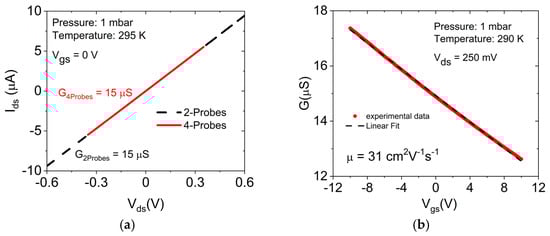
Figure 2.
(a) output curves measured in two- and four-probe configurations. (b) transfer curve showing p-type behaviour and field-effect mobility of 31 .
Figure 2b, shows an increasing conductance G when the temperature T is raised from 100 K to 400 K revealing the semiconducting nature of the nanosheet. The transfer characteristics, where is the channel conductance at fixed drain voltage, reported in Figure 2b confirm the semiconducting nature of the channel and reveals that it has a p-type behavior, as the channel conductance decreases for positively increasing gate voltage. The p-type doping of the PtSe2 channel can be attributed to O2 adsorbates [6,16,17,18] as well as to Pt vacancies [19]. Furthermore, the use of Ni as the contact material facilitates hole injection as the Ni Fermi level aligns to the top of the valence band of PtSe2.
We evaluated the field-effect mobility as (and are the drain current and voltage, is the capacitance per area, and are the channel length and width). The value of at room temperature is higher than that measured in differently fabricated PtSe2 devices [5,12] or in similar devices with other TMDs such as, or [16,20,21].
3.2. Photoresponse
The effect of light on nanosheets was investigated by illuminating the device with a supercontinuous white laser (450–2400 nm), with light pulses of given time duration and intensity. Figure 3a,b show the device channel current under fixed bias conditions for switching light at the intensity of 30 , in air at room pressure and at 1 mbar, respectively.
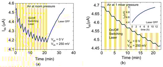
Figure 3.
(a) drain current subjected to switching light pulses (30 mW/cm2), monitored in air at room pressure. (b) drain current subjected to switching light pulses (30 mW/cm2), monitored in air at mbar pressure.
After a sequence of 12 pulses, 2 min long, the laser is switched off and the current is monitored in dark. Surprisingly, each laser pulse provokes a reduction of the current. Such behavior, which is referred to as negative photoconductivity, is opposite to the current increase normally observed under the light as an effect of electron–hole (e-h) pair photo-generation [22,23,24]. We point out that current reduction is a reversible phenomenon as the device returns slowly to the pre-irradiation state when the light source is turned off, with recovery significantly faster in air at room pressure.
The negative photoconductivity could be caused by a photogating effect due to charge trapping in the layer and light-induced oxygen desorption [25,26].
Holes photogenerated in the Si substrate and in the channel can be trapped in the gate dielectric and act as a positive gate that lowers the channel conductance of the p-type transistor. Simultaneously, electrons in (and perhaps ) molecules adsorbed over the channel can be excited by light into the channel. The neutralized molecules can be easily desorbed causing a decrease of the channel doping, hence of its conductivity. Both charge trapping and desorption decrease the current by a mechanism that is reversible with characteristic time depending on hole detrapping and adsortpion. Obviously, oxygen adsorption is facilitated at room pressure, thus explaining the faster recovery in air at room pressure.
4. Conclusions
In conclusion, we investigated the electrical transport in layers used as the channel of back-gated field-effect transistors. The transistor transfer characteristic indicated p-type conduction with mobility up to at room temperature. Exposure to light showed a dominant photogating effect, due to charge storage in the SiO2 dielectric and light-induced desorption of adsorbates that cause negative photoconductivity.
Author Contributions
Conceptualization, A.D.B. and P.K.H.; methodology, A.D.B., F.G., N.M.; software, A.P., A.G. and F.G.; validation, A.D.B. and F.G.; formal analysis, F.U., E.F. and F.G.; investigation, F.U., A.P., A.G., E.F. and F.G.; resources, A.D.B. and P.K.H.; data curation, F.U., F.G., N.M., A.G., A.P. and E.F.; writing—original draft preparation, A.D.B.; writing—review and editing, A.D.B., F.G.; sample fabrication, F.G. and N.M.; supervision, A.D.B.; project administration, A.D.B., F.G. and P.K.H.; funding acquisition, P.K.H., N.M., F.G. and A.D.B. All authors have read and agreed to the published version of the manuscript.
Funding
This work was partially funded by MIUR, projects Pico & Pro ARS01_01061 and RINASCIMENTO ARS01_01088. Science Foundation Ireland (SFI) through grants 15/IA/3131 and 12/RC/2278 and 15/SIRG/3329, 12/RC/2278_P2.
Conflicts of Interest
The authors declare no conflict of interest.
References
- Huang, J.; Yang, L.; Liu, D.; Chen, J.; Fu, Q.; Xiong, Y.; Lin, F.; Xiang, B. Large-area synthesis of monolayer WSe2 on a SiO2/Si substrate and its device applications. Nanoscale 2015, 7, 4193–4198. [Google Scholar] [CrossRef] [PubMed]
- Urban, F.; Passacantando, M.; Giubileo, F.; Iemmo, L.; Di Bartolomeo, A. Transport and Field Emission Properties of MoS2 Bilayers. Nanomaterials 2018, 8, 151. [Google Scholar] [CrossRef] [PubMed]
- Iemmo, L.; Urban, F.; Giubileo, F.; Passacantando, M.; Di Bartolomeo, A. Nanotip Contacts for Electric Transport and Field Emission Characterization of Ultrathin MoS2 Flakes. Nanomaterials 2020, 10, 106. [Google Scholar] [CrossRef] [PubMed]
- Di Bartolomeo, A.; Urban, F.; Passacantando, M.; McEvoy, N.; Peters, L.; Iemmo, L.; Luongo, G.; Romeo, F.; Giubileo, F. A WSe2 vertical field emission transistor. Nanoscale 2019, 11, 1538. [Google Scholar] [CrossRef]
- Yim, C.; Passi, V.; Lemme, M.C.; Duesberg, G.S.; Ó Coileáin, C.; Pallecchi, E.; Fadil, D.; McEvoy, N. Electrical devices from top-down structured platinum diselenide films. npj 2D Mater. Appl. 2018, 2, 5. [Google Scholar] [CrossRef]
- Di Bartolomeo, A.; Pelella, A.; Liu, X.; Miao, F.; Passacantando, M.; Giubileo, F.; Grillo, A.; Iemmo, L.; Urban, F.; Liang, S.-J. Pressure-Tunable Ambipolar Conduction and Hysteresis in Thin Palladium Diselenide Field Effect Transistors. Adv. Funct. Mater. 2019, 29, 1902483. [Google Scholar] [CrossRef]
- Di Bartolomeo, A.; Urban, F.; Pelella, A.; Grillo, A.; Passacantando, M.; Liu, X.; Giubileo, F. Electron irradiation of multilayer PdSe2 field effect transistors. Nanotechnology 2020, 31, 375204. [Google Scholar] [CrossRef] [PubMed]
- Guo, G.Y.; Liang, W.Y. The electronic structures of platinum dichalcogenides: PtS2, PtSe2 and PtTe2. J. Phys. C Solid State Phys. 1986, 19, 995–1008. [Google Scholar] [CrossRef]
- Fang, L.; Liang, W.; Feng, Q.; Luo, S.-N. Structural engineering of bilayer PtSe 2 thin films: A first-principles study. J. Phys. Condens. Matter 2019, 31, 455001. [Google Scholar] [CrossRef]
- Yim, C.; McEvoy, N.; Riazimehr, S.; Schneider, D.S.; Gity, F.; Monaghan, S.; Hurley, P.K.; Lemme, M.C.; Duesberg, G.S. Wide Spectral Photoresponse of Layered Platinum Diselenide-Based Photodiodes. Nano Lett. 2018, 18, 1794–1800. [Google Scholar] [CrossRef]
- Huang, Z.; Zhang, W.; Zhang, W. Computational Search for Two-Dimensional MX2 Semiconductors with Possible High Electron Mobility at Room Temperature. Materials 2016, 9, 716. [Google Scholar] [CrossRef] [PubMed]
- Jiang, W.; Wang, X.; Chen, Y.; Wu, G.; Ba, K.; Xuan, N.; Sun, Y.; Gong, P.; Bao, J.; Shen, H.; et al. Large-area high quality PtSe2 thin film with versatile polarity. InfoMat 2019, 1, 260–267. [Google Scholar] [CrossRef]
- Zhao, Y.; Qiao, J.; Yu, Z.; Yu, P.; Xu, K.; Lau, S.P.; Zhou, W.; Liu, Z.; Wang, X.; Ji, W.; et al. High-Electron-Mobility and Air-STable 2D Layered PtSe2 FETs. Adv. Mater. 2017, 29, 1604230. [Google Scholar] [CrossRef] [PubMed]
- Yim, C.; Lee, K.; McEvoy, N.; O’Brien, M.; Riazimehr, S.; Berner, N.C.; Cullen, C.P.; Kotakoski, J.; Meyer, J.C.; Lemme, M.C.; et al. High-Performance Hybrid Electronic Devices from Layered PtSe 2 Films Grown at Low Temperature. ACS Nano 2016, 10, 9550–9558. [Google Scholar] [CrossRef]
- O’Brien, M.; McEvoy, N.; Motta, C.; Zheng, J.-Y.; Berner, N.C.; Kotakoski, J.; Elibol, K.; Pennycook, T.J.; Meyer, J.C.; Yim, C.; et al. Raman characterization of platinum diselenide thin films. 2D Mater. 2016, 3, 021004. [Google Scholar] [CrossRef]
- Urban, F.; Martucciello, N.; Peters, L.; McEvoy, N.; Di Bartolomeo, A. Environmental Effects on the Electrical Characteristics of Back-Gated WSe2 Field-Effect Transistors. Nanomaterials 2018, 8, 901. [Google Scholar] [CrossRef]
- Giubileo, F.; Grillo, A.; Iemmo, L.; Luongo, G.; Urban, F.; Passacantando, M.; Di Bartolomeo, A. Environmental effects on transport properties of PdSe2 field effect transistors. Mater. Today Proc. 2020, 20, 50–53. [Google Scholar] [CrossRef]
- Bartolomeo, A.D.; Giubileo, F.; Romeo, F.; Sabatino, P.; Carapella, G.; Iemmo, L.; Schroeder, T.; Lupina, G. Graphene field effect transistors with niobium contacts and asymmetric transfer characteristics. Nanotechnology 2015, 26, 475202. [Google Scholar] [CrossRef]
- Ansari, L.; Monaghan, S.; McEvoy, N.; Coileáin, C.Ó.; Cullen, C.P.; Lin, J.; Siris, R.; Stimpel-Lindner, T.; Burke, K.F.; Mirabelli, G.; et al. Quantum confinement-induced semimetal-to-semiconductor evolution in large-area ultra-thin PtSe2 films grown at 400 °C. npj 2D Mater. Appl. 2019, 3, 33. [Google Scholar] [CrossRef]
- Pelella, A.; Kharsah, O.; Grillo, A.; Urban, F.; Passacantando, M.; Giubileo, F.; Iemmo, L.; Sleziona, S.; Pollmann, E.; Madauß, L.; et al. Electron Irradiation of Metal Contacts in Monolayer MoS2 Field-Effect Transistors. ACS Appl. Mater. Interfaces 2020, acsami.0c11933. [Google Scholar] [CrossRef]
- Di Bartolomeo, A.; Urban, F.; Pelella, A.; Grillo, A.; Iemmo, L.; Faella, E.; Giubileo, F. Electrical transport in two-dimensional PdSe2 and Mos2 nanosheets. In Proceedings of the 2020 IEEE 20th International Conference on Nanotechnology (IEEE-NANO), Montreal, QC, Canada, 29–31 July 2020; IEEE: Piscataway, NJ, USA, 2020; pp. 276–281. [Google Scholar]
- Zeng, L.-H.; Lin, S.-H.; Li, Z.-J.; Zhang, Z.-X.; Zhang, T.-F.; Xie, C.; Mak, C.-H.; Chai, Y.; Lau, S.P.; Luo, L.-B.; et al. Fast, Self-Driven, Air-Stable, and Broadband Photodetector Based on Vertically Aligned PtSe2/GaAs Heterojunction. Adv. Funct. Mater. 2018, 28, 1705970. [Google Scholar] [CrossRef]
- Di Bartolomeo, A.; Luongo, G.; Iemmo, L.; Urban, F.; Giubileo, F. Giubileo Graphene–Silicon Schottky Diodes for Photodetection. IEEE Trans. Nanotechnol. 2018, 17, 1133–1137. [Google Scholar] [CrossRef]
- Liu, G.Z.; Zhao, R.; Qiu, J.; Jiang, Y.C.; Gao, J. Negative photoconductivity under visible light illumination in LaAlO3/SrTiO3 heterostructures. J. Phys. D Appl. Phys. 2019, 52, 095302. [Google Scholar] [CrossRef]
- Francinelli, A.; Tonneau, D.; Clément, N.; Abed, H.; Jandard, F.; Nitsche, S.; Dallaporta, H.; Safarov, V.; Gautier, J. Light-induced reversible conductivity changes in silicon-on-insulator nanowires. Appl. Phys. Lett. 2004, 85, 5272–5274. [Google Scholar] [CrossRef]
- Cadiz, F.; Robert, C.; Wang, G.; Kong, W.; Fan, X.; Blei, M.; Lagarde, D.; Gay, M.; Manca, M.; Taniguchi, T.; et al. Ultra-low power threshold for laser induced changes in optical properties of 2D molybdenum dichalcogenides. 2D Mater. 2016, 3, 045008. [Google Scholar] [CrossRef]
Publisher’s Note: MDPI stays neutral with regard to jurisdictional claims in published maps and institutional affiliations. |
© 2020 by the authors. Licensee MDPI, Basel, Switzerland. This article is an open access article distributed under the terms and conditions of the Creative Commons Attribution (CC BY) license (https://creativecommons.org/licenses/by/4.0/).