Abstract
Nowadays, the development of efficient water treatment processes is increasingly driven by the need to provide solutions for contaminants of emerging concern. Electrochemical advanced oxidation processes (EAOPs) based on diamond electrodes can be part of innovative removal concepts. However, expensive substrates, energy-intensive chemical vapor deposition (CVD) of diamond, and market availability complicate matters for diamond electrodes to gain traction in the water treatment sector. In addition, it has to be stated that the mining and complex processing of necessary substrates like Si, Ti, Nb, or Ta need a significant amount of fresh water, which counteracts the need for more sustainability in the field of EAOPs. In this context, a ceramic-based boron-doped diamond (BDD) electrode is presented, which addresses this dilemma. The presented concept of the so-called interdigitated double diamond electrode (iDDE) consumes 14–46% less energy in batch-mode experiments to degrade an organic model molecule compared to standard BDD technology in a poorly conductive electrolyte (κ < 350 µS/cm). Laser-induced micro-structuring of the BDD layer reduces the interelectrode spacing (IES) of the iDDE to below 50 µm. The structuring approach at the micrometer scale enables the treatment of electrically low-conductivity electrolytes more energy efficiently, while reducing the need for a supporting electrolyte or a proton exchange membrane. Degradation experiments and Raman measurements reveal different properties of an iDDE compared to standard BDD technology. The iDDE concept highlights the need to understand the significance of non-uniform current density distributions on the general electrochemical activity of BDD electrodes.
1. Introduction
In recent years, it has become apparent that conventional water treatment processes are no longer sufficient for removing pollutants from wastewater. Increasing anthropogenic pollution and the partially permanent environmental impact have become a major threat to mankind. The widespread detection of drug residues, multi-resistant germs, and polyfluorinated compounds, so-called “forever chemicals” in surface waters, emphasizes this challenge [,,]. Standardized physicochemical and biological treatments often cannot ensure the removal of such contaminants. Therefore, an additional cleaning process becomes necessary. Advanced oxidation processes (AOPs) are one approach to face those challenges [].
In electrochemical advanced oxidation processes (EAOPs), highly oxidative species are produced due to advanced water electrolysis. In addition to the classical electrolysis products, hydrogen and oxygen, hydroxyl radicals (•OH) form. Electrode materials with high overpotentials for oxygen evolution are capable of producing physiosorbed •OH on the anodic surface, facilitating complete mineralization of organic compounds. Only a few so-called “non-active” electrode materials show this behavior, like PbO2 and SnO2-Sb-doped or boron-doped diamond (BDD) []. In the case of non-active electrodes, the discharge of the water molecule into a •OH is characterized by a weak interaction between the anode surface and •OH. This allows the •OH to be available for the combustion of organic compounds [,,]. In the past decade, BDD electrodes have experienced increasing interest from all kinds of fields, like anodic wastewater treatment, electrochemical sensing, or cathodic CO2 reduction []. However, the energy-intensive production combined with the use of conflictual and expensive substrates like niobium or tantalum makes their use extremely controversial []. A new generation of BDD electrodes could pave the way to establish BDD technology in the field of water purification.
In general, electrode systems are based on two parallel-arranged conductive plates or meshes with an interelectrode spacing (IES) in the range of 500 µm up to several centimeters. To receive a specific current and, therefore, a defined electrode activity, the applied voltage heavily depends on the electrical conductivity of the chosen electrolyte and IES. As the IES decreases, the influence of the electrolyte conductivity on the electrode activity becomes negligible. This assumption is also utilized in proton exchange membrane electrolysis, where the membrane defines the distance between the anode and the cathode and functions as an ionic charge carrier [,]. Electrically conductive diamond coatings are typically deposited on carbide-forming metallic substrates or doped silicon, where the electron conduction primarily occurs in the substrate. In the literature, electrically non-conductive substrates for BDD electrodes are rarely studied; however, these BDD electrodes can also be used as sensors or, in the form of macroporous electrodes, for wastewater treatment based on alumina [,]. This work features a novel electrode design based on a BDD coating produced by chemical vapor deposition (CVD) on a non-conductive ceramic substrate. Both anode and cathode are made of BDD and are less than 50 µm apart, with no need for an ion exchange membrane due to a micro-structuring approach. The degradation experiments are based on the oxidation of the ring molecule glucose, which serves as an organic model molecule to investigate the capability to decrease the chemical oxygen demand (COD). The innovative electrode concept of this study could significantly reduce the production and operating cost of BDD electrodes for specific applications, increase their availability, and limit their environmental footprint, leading to new opportunities for diamond electrodes in the field of advanced water treatment technologies.
2. Materials and Methods
2.1. Fabrication of Ceramic-Based Planar Diamond Electrodes
The BDD layer was deposited in a custom-built hot-filament CVD (HFCVD) coating machine. The ceramic substrate (5 cm × 5 cm × 0.25 cm with 4 × Ø4 mm holes in the corners for electrical contacting, kaolinite–cordierite mass, Fly for Design 1 GmbH, Schönwald, Germany) is aligned between two parallel rows of filaments. The filament arrays are 30 mm apart, and the samples are placed in between. Up to 18 samples can be coated at once with the used coating setup (42 cm × 22 cm), ensuring comparability of multiple samples. The deposition temperature was regulated at 850 ± 10 °C with the filament-induced (10 W/cm2) activation of the hydrogen-based (1000 mL/min) reactive gas phase consisting of methane (12 mL/min) and trimethylborate (0.15 mL/min) at a pressure of 3.3 mbar. To ensure good layer adhesion and homogeneous diamond growth, the ceramic substrates were particle-blasted in advance (SiC-F150, 4 bar), ultrasonically cleaned in ethanol, and seeded with nano-diamond (Carbodeon, uDiamond Hydrogen-D, Vantaa, Finland, 1:500 in ethanol). To produce a diamond layer thickness of around 7 µm with a microcrystalline morphology with crystal facets larger than 1 µm, a 42 h-long coating time was chosen, which resulted in a growth rate of 0.17 µm/h.
To manufacture the new electrode design, a selective removal of the coated BDD layer was conducted with an infrared structuring laser (Rofin 100D, Coherent Corp., Saxonburg, Pennsylvania, λ = 1064 µm, 100 W, F240, 10 kHz, 60 mm/s). The total structural length of the laser-structured path was 233.8 cm for each sample side, and the IES was around 50 µm. The detailed structuring design is shown in S1 of the Supporting Information. After laser-structuring, the electrically separated areas were electrochemically anodized at 10 V in distilled water for 2 min to remove potential sp2 carbon residues within the laser-structured gap. For comparison and characterization, another iDDE with an IES of 20 µm was structured by Novanta Photonics (Artos laser, Wackersdorf, Germany, λ = 1064 µm).
2.2. Characterization of the BDD Electrode
Scanning electron microscopy (SEM), laser-scanning microscopy (LSM), Raman spectroscopy, X-ray diffraction (XRD), and stereographic imaging were used to characterize the BDD and its substrate. Refer to Supporting Information S2 for details.
2.3. Electrochemical Testing Setup
All chemicals (NaCl, CuSO4 ∙ 5H2O, and C6H12O6) used for testing were of practical grade from Carl Roth GmbH + Co. KG (Karlsruhe, Germany). Electrochemical degradation experiments were carried out in batch mode, with an electrolyte volume of 250 mL, while constantly homogenized with a magnetic stirrer (150 rpm) at 20 ± 1.5 °C within a water bath. Ultra-purified water (κ = 0.05 µS/cm, 18.2 MΩ cm) with 20 mg/L chloride and 1 g/L glucose functioned as base electrolyte. The degradation tests were performed in a current-controlled manner at 0.5 A for 3 h, corresponding to a total specific charge of 6 Ah/L. All degradation experiments were conducted with an iDDE that had an IES of 50 µm. For comparison, a standard electrode setup with BDD on silicon (BDD-Si, ~7 µm BDD layer thickness) as anode (5 cm × 5 cm × 0.3 cm) and a V2A steel plate as cathode (5 cm × 5 cm × 0.1 cm) was used (IES = 800 µm). Boromond (Changsha, China) was the supplier for a commercially available BDD-Si electrode. Both electrodes were contacted with titanium stripes (Grade 2, 10 cm × 1 cm × 0.1 cm) as a current collector. The voltage applied for the iDDE ranged from 7.1 to 8.0 V, while for the BDD-Si/Steel combination, it ranged from 9.8 to 11.8 V. Please refer to the Supporting Information S3 for the exact electrode configuration. The two electrode setups were tested simultaneously, sharing the same water bath to equalize the electrolyte temperature between both electrode configurations. Each electrolysis experiment was repeated three times to ensure reproducibility. COD was measured using photometric cuvette tests (NANOCOLOR CSB 1500, 100–1500 mg/L O2) from Machery-Nagel (Düren, Germany) and analyzed with the NANOCOLOR UV/VIS II spectrophotometer.
To cathodically deposit copper from a copper(II)-sulfate pentahydrate solution (0.0015 mol/L), a voltage of 2 V (5 mA) was applied at the iDDE for 5 min. The scale formation experiment was performed in tap water for 12 h with an applied current of 0.5 A at 20 ± 1.5 °C. Refer to the Supporting Information S4 for the electrolyte composition.
3. Results and Discussion
3.1. The Concept of an Interdigitated Double Diamond Electrode (iDDE)
The idea of an all-diamond electrode is well described in the literature for the purpose of electrochemical sensing with either a microelectrode array [,,,] or needle-shaped electrode [,]. In general, an undoped diamond (UDD) layer insulates the conducting BDD. In most cases, a combination of multiple processing steps, such as the CVD of BDD and UDD, lithographic techniques, precise laser-structuring, or ion beam cutting, is needed to manufacture all-diamond electrode systems. In the case of the electrode design for this study, a BDD layer with a thickness of 6–8 µm is deposited on a non-conductive ceramic-based substrate. A selective removal of well-defined regions splits the electrically conductive diamond layer into two or multiple electrically separated areas, as shown in Figure 1a.
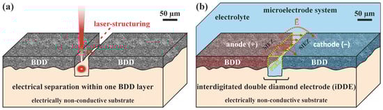
Figure 1.
Concept of an interdigitated double diamond electrode (iDDE). (a) Electrically conductive BDD layer structured and electrically separated by a laser beam. (b) iDDE with a schematically depicted electric field (red arrows), while applying a voltage in an electrolyte. The electrochemically active sites of the iDDE can be divided into a primary and a secondary interelectrode zone (PIEZ, SIEZ). The yellow dotted line highlights the PIEZ.
The laser beam, used for structuring in this case, simply burns the diamond, producing CO2 and the stable carbon phase graphite. Afterwards, neighboring BDD segments are electrically separated. Sbartai et al. [] proposed a microcell for metal-ion sensing, including multiple electrodes within one BDD layer (300 nm thick) on an insulated silicon wafer with a similar approach to detect currents in the nA range. In this work, the laser-structuring of the BDD layer on a non-conductive substrate is a simple and flexible way to manufacture all-diamond multielectrode arrays. The working anode (+) and counter cathode (−) are located in the same geometrical plane, building a pseudo-2D electrode system. Therefore, this configuration is described as an interdigitated double diamond electrode (iDDE) system.
With the addition of an electrolyte, the laser-structured gap of the iDDE functions as a microreaction chamber for electrochemical processes, as shown in Figure 1b. The electric field builds up similarly to a capacitor plate, resulting in parallel electric field lines within the laser-structured trench between anode (+) and cathode (−). However, the electric field becomes inhomogeneous close to the structured edges and in the peripheral area of the sample. The peripheral area accounts for the nominal dimensions of the substrate. The electrolyte volume directly in contact with the nominal electrode surfaces of the cathode and anode can also be described as the secondary interelectrode zone (SIEZ), while the zone immediately within the laser-cut gap can be referred to as the primary interelectrode zone (PIEZ). The strongest electric field is expected to be built up directly in the laser-structured trench, defining the main location for electrochemical reactions.
Due to its small IES in the range of 20–50 µm, the iDDE can be called a microelectrode and is especially designed for lower conductive electrolytes like drinking water, which is still a major hurdle for conventional BDD technology today [,]. Comparable electrode spacings can be found in electrode systems equipped with proton exchange membranes, microelectrode arrays for sensing, or disinfection devices [,,].
3.2. Characterization of the iDDE
A tip of the “finger-like” network structure used to fabricate the iDDE is shown in Figure 2. The LSM images illustrate the working principle of the iDDE concept. The laser-structured trench between cathode and anode is in the range of 20–50 µm for samples in this study. The trench and, therefore, the IES between cathode and anode is 20–25 µm wide in the case of Figure 2 and has an average depth of 30 µm. The laser does not just ablate the diamond layer (7 ± 0.5 µm) but also penetrates deep into the ceramic substrate. The space that is directly defined by the width and length of the laser-cut gap is the PIEZ, as the minimal interelectrode distance is solely determined by the resolution of the chosen structuring system. The reaction space above the nominal surfaces of the anode and cathode, on the other hand, represents the SIEZ. Fundamentally, the zones differ due to distinct distances between the cathode and the anode; while the IES should be constant in the case of the PIEZ, it is larger and variable in the case of the SIEZ, depending on the reaction site considered.
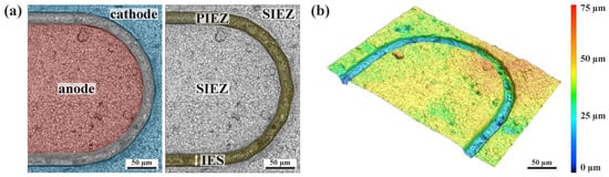
Figure 2.
(a) LSM image of an anodic fingertip of an interdigitated double diamond electrode (iDDE). The laser-structured trench electrically separates the anode from the cathode (artificially colored). The interelectrode spacing (IES) is in the range of 20–25 µm. The primary interelectrode zone (PIEZ) covers the electrolyte volume within the laser-structured gap, whereas the secondary interelectrode zone (SIEZ) describes the volume above the nominal surfaces of anode and cathode. (b) Colored LSM image of the topography of an iDDE.
The rough topography of the BDD layer is characterized by Rz = 22.2 ± 0.9 µm and Ra = 2.2 ± 0.1 µm. This is mainly a result of the particle blasting of the ceramic as a necessary pretreatment step before CVD coating to ensure sufficient mechanical bonding of the BDD layer to its substrate. For a stable and long-lasting bond between the diamond layer and the ceramic substrate, the CVD diamond coating must be deposited as stress-free as possible. Residual stresses between the diamond and the ceramic substrate caused by different thermal expansion coefficients during the cooldown step after coating cannot be compensated by plastic deformation. Accordingly, it is necessary to use a substrate that has a similar coefficient of thermal expansion (α) to polycrystalline CVD diamond in the corresponding process window to prevent the stress-induced delamination of the diamond layer. Doping with boron complicates the analysis of potential stresses by Raman spectroscopy, as the one-phonon band Raman peak shifts to lower wavenumbers and becomes asymmetrical with increasing boron content due to the Fano interference []. Therefore, a UDD layer was prepared to characterize potential residual stresses. Raman data shown in Figure 3a indicate no stresses higher than 1 GPa (calculated after Anastassakis et al. []) in the UDD layer on the cordieritic substrate due to no major Raman shift (+1 cm−1) of the diamond signal (sp3 carbon) at wavenumber 1332 cm−1. Similar thermal expansion behavior within the relevant coating temperature interval (35–850 °C) between the diamond coating (α = 3.5 × 10⁻⁶/K for polycrystalline CVD diamond []) and the cordieritic substrate (α = 3.6 × 10⁻⁶/K) reduces potential residual stresses. The maximal residual stresses of 1 GPa are relatively low compared to metallic or semi-metallic substrates with compressive stress > 3 GPa [,,]. Non-conductive substrates like silica or alumina are not suitable for this type of planar electrode due to their high thermal expansion exceeding α = 5 × 10⁻⁶. Cordierite is well known and established for applications in need of low thermal expansion, being a good match for polycrystalline CVD diamond. Graphite impurities within the UDD layer are characterized by the G-band at around 1545 cm−1.
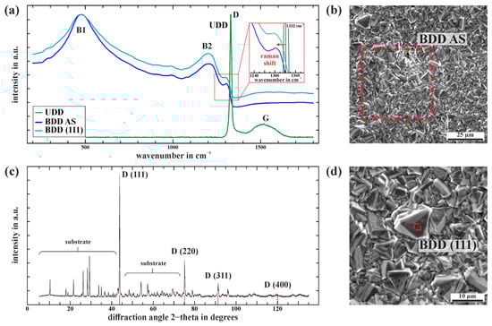
Figure 3.
(a) Raman spectra of the BDD layer of an iDDE (BDD AS), a (111) facet within, and an undoped diamond layer (UDD) on the same cordieritic substrate. (b) SEM image of the BDD of an iDDE. The dotted red line highlights the scanned area by Raman spectroscopy (BDD AS). (c) XRD-spectra of the iDDE with distinct diamond (D) and substrate peaks. (d) SEM image of the BDD of an iDDE with a focus on the analyzed (111) facet by Raman spectroscopy highlighted in red.
Raman spectra of an area scan (BDD AS) of the grown BDD layer of an iDDE and an averaged scan of a (111) facet are also shown in Figure 3a. Both spectra exhibit similar trends with a characteristic diamond peak at around 1306 cm−1 and less resolved peaks for boron at around 480 cm−1 (B1) and 1200 cm−1 (B2). The BDD Raman data refer to the microcrystalline diamond shown in Figure 3b within the SIEZ of Figure 2a. The polycrystalline BDD layer predominantly exhibits a (111) morphology with pronounced twinning while crystal facets reach up to 5 µm in size. The diamond diffractions in the XRD spectra correspond to (111), (220), (311), and (400) planes, while (111) has the highest intensity of all (comp. Figure 3c). The unspecified XRD peaks originate from the cordieritic substrate. The SEM images (Figure 3b,d) confirm the predominance of the (111) morphology in combination with (110). Surfaces with (111) orientation are known to be more electrochemically active compared to (100) faces due to higher boron incorporation during the CVD process and, therefore, exhibit higher electrical conductivity [,,,]. The minor deviations in the Raman signal of a single (111) facet (comp. Figure 3d) compared to the large area scan (BDD AS) support a significant incorporation of boron within the grown BDD layer.
3.3. Local Current Density Distribution at the iDDE
Current density is one of the most important parameters to be specified when carrying out electrochemical experiments. The amount of current flowing over a defined area is equivalent to the electrochemical activity. However, the global current density is insufficient in describing the local current density distribution in many electrolytic setups, especially in the case of an iDDE. The accurate description of the electrochemically active surface area becomes very complex quite fast, because in many cases standard analytics, such as the Randles–Ševčík equation, cannot be applied []. Additionally, the examination of the local current density distribution is scarcely present and rarely discussed in BDD literature, despite their significant impact [,].
The local current density distribution at an iDDE can be primarily divided into two different regimes. The PIEZ of an iDDE represents the zone with the lowest ohmic resistance within the electrolyte. The narrower the laser-structured gap, the stronger the electric field between the BDD anode and BDD cathode within the PIEZ. The majority of the relevant electrochemically active surface area is, therefore, exclusively defined by the layer thickness of the deposited BDD, the structure length that separates anode and cathode, the homogeneity of the structuring itself, and the IES. The relevance of the PIEZ for the electrochemical activity of the iDDE can be visually demonstrated through cathodic Cu deposition, as shown in Figure 4. Electroplating is based on the assumption that the deposition rate is enhanced with increasing current density and can be homogenized through a constant electric field or uniform current density distribution. The cathodic Cu deposition is primarily detectable within the PIEZ on the cathode of the iDDE, hinting towards a non-uniform current density distribution at an iDDE.
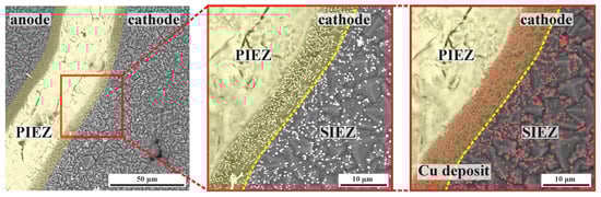
Figure 4.
SEM images of a cathodic Cu deposition at an iDDE via the detection of backscattered electrons. The PIEZ is artificially colored yellow. A dotted yellow line separates the PIEZ and the SIEZ. The deposited copper is artificially colored red on the right-hand side.
There was a smaller amount of Cu deposits within the SIEZ due to higher overall IES. By increasing the average IES, the reactivity of the corresponding BDD site decreases. Graphical analysis of the distribution of the cathodic Cu deposition places the reactivity maximum within the PIEZ and minor activity in the SIEZ, with an approximated reaction ratio of 4:1. Based on this assumption, Table 1 summarizes the expected currents and current densities for degradation experiments in this study, which were conducted at 0.5 A.

Table 1.
Approximation of the theoretical local current density at the primary interelectrode zone (PIEZ) of an iDDE with 7 ± 0.5 µm BDD layer thickness, 467.6 cm structure length, an interelectrode spacing of 50 µm, 49 cm2 global surface area (Aanode), and a PIEZ/SIEZ reaction ratio of 4:1. The thickness of the sample, surface roughness, edge effects, and the surface coverage by contacts are excluded from this consideration.
The local current density within the PIEZ is massively elevated (j = 1.22 A/cm2) relative to the global current density (j = 0.01 A/cm2), which is associated with the nominal electrode dimensions and, therefore, the SIEZ. Exceeding the global current density by roughly a factor of 120, as shown in Table 1, should be understood as a geometry-based approximation of the local current density within the PIEZ of an iDDE for this specific configuration. Such high current densities in the field of electrochemistry are found in specialized applications, such as electrochemical ozone production [,].
Figure 5a shows a cross-section within the PIEZ focusing on the laser-structured diamond layer. A columnar growth of the HFCVD diamond layer is partially discernible, and the surface appears etched. The underlying ceramic shows evidence of a localized melting event caused by the laser-structuring process. The structuring exposes the entire growth history of the CVD diamond layer, which begins with nano-diamond seeds (1), progresses through columnar diamond growth (2), and leads to microcrystalline grains with facet sizes up to 5 µm (3). Accordingly, the Raman analysis from Figure 3a is insufficient in characterizing the diamond within the PIEZ, which plays the crucial role for the evolution of the electric field, determining the current density distribution j at an iDDE.
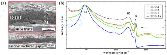
Figure 5.
(a) Cross-sectional SEM image of the laser-structured BDD layer within the PIEZ of an iDDE. (b) Raman spectra within the PIEZ according to (a) and an area scan (BDD AS) of the BDD surface within the SIEZ (compare Figure 3a).
Raman measurements (comp. Figure 5b) within the gap show a difference in their diamond quality compared to the surface (BDD AS), but also differ among themselves depending on the position in the grown layer. The measurement of the Raman signals of the BDD within the PIEZ (BDD 1–3) results in a more distinct sp3 carbon signal for the one-phonon diamond line with reduced asymmetry. Additionally, the peak shift is less pronounced compared to the area scan from the SIEZ (BDD AS). The differences observed between BDD 1, 2, and 3 are explained by the intersectional analysis of the CVD growth history, which provides insight into various grains and their orientations. Due to the dominance of (111) facets on the growth surface (SIEZ), perpendicular facets are particularly expected within the PIEZ. Significant differences in the doping level and sp3/sp2 carbon ratios across the growth history also cannot be ruled out, directly influencing the electrochemical properties of BDD [,,]. The presented Raman spectra illustrate an even more complex picture of the current density distribution at an iDDE and the variation in electrochemically active surfaces present.
The inhomogeneous local current density distributions at an iDDE are also characterized by the accumulation of edge effects due to the laser-structuring approach and laser ablation irregularities. Elevated current density at electrode edges is known and described in the literature [,]. However, the local current density distribution is not only influenced by the geometry of the electrode system but also affected by the electrolyte conductivity, hydrodynamics, and electrode overpotentials []. The understanding of non-uniform local current density distribution is crucial to predicting the type and quantity of forming oxidation products during an EAOP, especially when working with mesh, zero-gap, ultra-nano-, or porous BDD electrodes. Those observations make it difficult to compare iDDE technology based on the global current density with standard 2D-BDD electrodes. Nevertheless, the consideration of the amount of charge, current efficiency, and the energy consumption to remove specific contaminants is one approach to comparing different EAOPs with each other and serves as a base for the following electrochemical testing, where glucose is degraded as an organic model molecule.
3.4. Capability of Glucose Oxidation with an iDDE
First electrochemical tests show considerable differences between a conventional planar electrode arrangement and an iDDE regarding the removal of glucose (1 g/L). While the overall degradation behavior over the amount of charge is almost identical for both setups, the energy consumption differs significantly, as can be seen in Figure 6a,b. To decrease the total COD by 75%, the BDD-Si/steel pairing needs 46% more energy than the iDDE setup. Adjusting the IES by more than an order of magnitude (800 µm for BDD-Si/steel => 40–50 µm for iDDE) reduces the overall energy consumption in this specific setup significantly. This makes the iDDE more applicable for low-conductivity electrolytes, which is considered to be imperative to maximize the technology readiness level of BDD electrodes []. In both cases, this study reports a falling instantaneous current efficiency (ICE) from the beginning of the experiment, as shown in Figure 6c. This indicates a mass transport-controlled degradation process. The ICE was calculated after Panizza and Cerisola [].
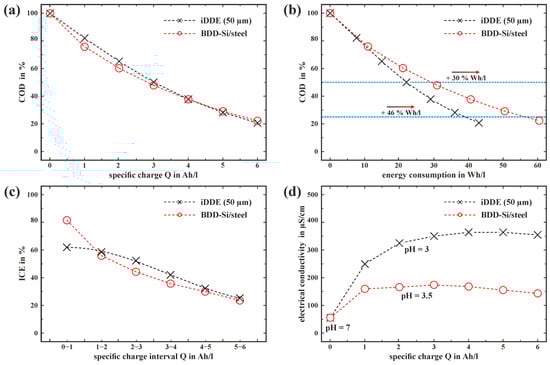
Figure 6.
COD degradation in % of 1 g/L glucose in 20 mg/L Cl− (aq) with an iDDE (50 µm) and BDD-Si/steel setup. (a) COD degradation in % plotted over the amount of specific charge Q in Ah/L and (b) energy demand in Wh/L. The blue dashed lines symbolize the 50 % and 75 % degradation threshold. (c) ICE evolution after [] and (d) electrolyte conductivity as a function of Q in Ah/L.
It should be noted that for the BDD-Si/steel configuration, the maximal measured ICE of 87% is significantly higher compared to the iDDE with an ICE of 62%, which can be explained by the different flow dynamics of each setup. An iDDE with a longer laser structure could counteract mass transport limitations due to the increase in the electrochemically active surface area within the PIEZ. Reducing the IES in the case of the BDD-Si/steel, on the other hand, would decrease the required voltage and thus reduce energy consumption for a given amount of charge. At the same time, the altered fluid dynamics may lead to poorer ICE due to mass transport limitations. The measurement of different electrolyte conductivities (κ) evolving during the EAOPs (comp. Figure 6d) is noticeable. While the conductivity in the case of BDD-Si/steel electrode setup increases to an average of up to 163 ± 6 µS/cm from the initial 55 ± 2 µS/cm, the conductivity of the electrolyte in the case of the iDDE reaches 320 ± 11 µS/cm after 1 Ah/L, leading to lower required voltage and, therefore, lower energy consumption. The main reason for the difference in energy efficiency is, therefore, attributed to varying electrolyte conductivities throughout the electrolysis experiment. Running the iDDE in the same electrolyte as the BDD-Si/steel configuration after finishing the degradation experiment (κ = ~163 µS/cm, Q = 6 Ah/L) suggests still 14% more energy efficiency in the case of the iDDE due to a lower required voltage for the same current. Degradation experiments within ultra-pure water (κ = 0.05 µS/cm) support this observation (compare S5).
Slightly lower evolving pH values during the electrolysis indicate higher proton concentrations of the iDDE electrolyte (pH = 3 iDDE vs. pH = 3.5 BDD-Si/steel after 2–3 Ah/L starting from pH = 7). There are several possible explanations for this phenomenon, including differences in diamond layer quality, the current density distribution, and different electrode configurations. Several studies have shown that the sp3/sp2 carbon ratio, the boron doping level, and crystal facet orientation significantly influence the oxidation behavior at BDD electrodes [,,,,]. An increasing graphitic (sp2 carbon) content results in the formation of more organic by-products instead of completely mineralizing the glucose. This is due to the occurring conversion reactions via direct oxidation instead of indirect oxidation through •OH. The significantly increased current density within the PIEZ of an iDDE inevitably leads to locally higher production of •OH at sp3 carbon sites. Increased amounts of •OH can result in higher degradation and mineralization efficiency []. The cathode materials used also differ in their overpotential for hydrogen evolution. While BDD exhibits a comparatively high overpotential, it is relatively low for V2A steel, which in turn could be a reason for higher proton concentration in the case of the iDDE electrolysis experiment.
3.5. Feasability and Applicability
The iDDE concept is based on a non-conductive substrate. Ceramic materials with appropriate thermal expansion matching the polycrystalline CVD diamond can be found worldwide and are available at a reasonable cost. Cordierite masses are commonly used in the automotive industry as catalytic converter material, as insulation material for ovens, or even as pizza stones. In contrast, the extraction and processing of standard substrates, such as Ti, Si, Nb, and Ta, is relatively complex and expensive. Furthermore, the corresponding mineral-containing ores are very rare, and some are even classified as conflict material []. In addition, metallic substrates are susceptible to hydrogen embrittlement, which may require protective interlayers or lower diamond CVD temperatures [,]. With a substrate temperature of approx. 850 °C for microcrystalline diamond growth on ceramics, a higher growth rate compared to Nb or Ti metal substrates can be achieved. This results in shorter coating times and, consequently, reduced coating costs. The iDDE concept also appears to be easily scalable in terms of both the number and size of the electrodes using HFCVD as a coating technique.
However, the applicability of all EAOPs primarily depends on the concentration of the pollutant load, which is particularly suitable within the range of 10–100,000 mg/L, with optimal performance between 100 and 10,000 mg/L []. In exceptional cases, the removal of just a few percent of COD can already achieve the experimental goal. Koch et al. [] have already demonstrated the disinfection potential of the iDDE technology by removing biofilms from dental implants. By introducing a variable structuring concept, iDDEs with different electrochemical behavior can be produced, despite having identical diamond quality and the same global current density. This would enable the configuration of iDDEs according to specific application cases, since the structuring design allows the customization of the local current density distribution to control oxidant formation, pollutant degradation, and disinfection potential. This way, BDD originating from a single CVD diamond coating can be used in different scenarios.
The iDDE has been shown to be a reasonable addition to existing standard electrode systems, especially in poorly conductive electrolytes (κ < 350 µS/cm). Even applications in ultra-purified water (κ = 0.05 µS/cm) become possible at acceptable voltages and energy consumptions (refer to S5). Alternative electrode setups for comparable treatment requirements feature the use of a zero-gap reactor design based on microporous materials []. The iDDE technology can thus contribute to closing the gap for the treatment of poorly conductive water matrices via BDD. The concept of an all-diamond electrode also allows polarity reversal during EAOP, which enables the removal of pH-dependent precipitates by switching the polarity. The iDDE anode can be clearly distinguished from the cathode during scale formation (comp. Figure 7). The option to switch polarity could increase the service life of an iDDE, as the cathodic load can be split up between two electrodes over time. In this case, alkaline pH, hydrogen evolution, and cathodic deposits (scale) are regarded as cathodic loads for both the ceramic substrate and the BDD coating.
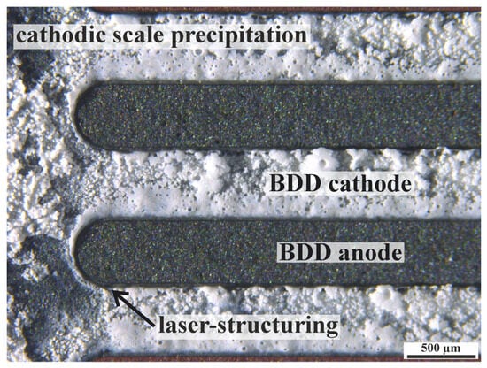
Figure 7.
Stereographic image of a cathodic scale precipitation on an iDDE in tap water as electrolyte.
3.6. Challenges and Outlook
In order to be able to use the iDDE in the application field of water purification or wastewater treatment, fundamental questions still need to be answered. BDD is not only capable of oxidizing harmful substances or eliminating germs, but it can also lead to toxic by-product formation. The oxidation of halides like chloride to chlorate and perchlorate is a widely discussed topic in the literature, and one of the biggest hurdles for the establishment of BDD electrodes in water treatment systems [,,,]. Chlorate and perchlorate have been proven to negatively affect human and animal metabolism. Therefore, the US Environmental Protection Agency mandated a limit of 15 µg/L perchlorate for drinking water []. In other words, this means a maximum of approx. 5 µg/L chloride may be converted to perchlorate (conversion factor 2.8) in order to just meet the specifications during EAOP. Elevated perchlorate concentration could pose significant problems for official approval or require further post-processing steps [,,,]. The hypothesized partially high local current density within the PIEZ of an iDDE could lead to an even further increased formation of perchlorate because standard BDD electrodes with relatively high global current densities applied have proven to do so []. It is expected that an iDDE-based system can produce perchlorate more efficiently due to the local increase in hydroxyl radical concentration within the PIEZ, but at the same time, an iDDE could produce a lower amount overall due to the relatively constrained electrochemically active surface area compared to standard BDD electrodes.
The sole electron conduction through the BDD coating limits the size and design of the electrodes, as increasing the layer dimensions leads to higher ohmic losses. The use of metallic thin films between the ceramic substrate and BDD or conducting top layers, like a combination of Ti and Au, would significantly increase the electron transport capacity of the iDDE. However, the electrochemical stability of a potential interlayer must be equivalent to that of a diamond, or the interlayer must be effectively isolated from the electrolyte. The long-term stability, in general, still needs to be evaluated. Laser-structuring induces a high density of structural defects and allows the electrolyte to reach the diamond–ceramic interface. This deliberately exposes the interface to the entire electrochemistry, like oxidation and reduction reactions, local extreme pH values, and gas formation. Through pores in the ceramic substrate or inhomogeneous diamond layer growth, electrolytes can also penetrate below the electrochemically active layer and induce or intensify potential corrosion and delamination processes. Nevertheless, it is already possible to carry out several 100 h of electrolysis with the iDDE in the postulated water matrix (20 mg/L chloride + 0–1 g/L glucose) at 0.5 A. However, further investigations are needed to understand potential failure mechanisms in the long run.
4. Conclusions
This work presents a novel planar microelectrode based on an all-diamond electrode approach. The chemical vapor deposition (CVD) of boron-doped diamond (BDD) on an electrically non-conductive substrate allows the electrical insulation of areas within the deposited BDD layer due to laser ablation. This enables the use of the structured BDD layer as a planar pseudo-2D microelectrode, a so-called interdigitated double diamond electrode (iDDE). Minimal interelectrode spacing < 50 µm can be achieved, enabling energy-efficient treatment of waters with electrical conductivity less than 350 µS/cm. The majority of electrochemical reactions take place in the laser-structured gap, although this significantly reduces the relevant electrochemically active surface area in contrast to the actual electrode size. The analyzed degradation behavior of an iDDE towards the oxidation of glucose is comparable to commercially available BDD electrodes, but more energy efficient. Raman data support a rather complex evolution of the electric field at an iDDE, especially within the laser-structured gap due to differences in CVD diamond quality. Inhomogeneous current density distributions with local maxima of j ≥ 1 A/cm2 are nothing unusual at an iDDE defining its electrochemical character. Nevertheless, the relatively easy production of an iDDE based on a ceramic substrate in combination with a highly flexible structuring approach could usher in a new era for more sustainable BDD electrodes.
5. Patents
The Friedrich-Alexander-Universität Erlangen-Nürnberg, Stefan Rosiwal, and Hanadi Ghanem have filed a patent based on the presented electrode concept, Patent number: WO2020/249519A1.
Supplementary Materials
The following supporting information can be downloaded at https://www.mdpi.com/article/10.3390/electrochem6040041/s1, S1–S5. S1: Interdigitated double diamond electrode: structuring design; S2: Characterization methods; S3: Electrode configurations; S4: Tap water composition; S5: Degradation experiment in ultra-purified water.
Author Contributions
Conceptualization: M.Z.; methodology (samples): J.B., L.H., C.M., and M.Z.; methodology (experiments): J.B., L.H., C.M., and M.Z., data curation: C.M. and M.Z., visualization: C.M. and M.Z., writing—original draft preparation: M.Z.; writing—review and editing: H.G., C.M., S.R., and M.Z.; supervision: S.R.; project administration: M.Z. All authors have read and agreed to the published version of the manuscript.
Funding
This study was financed by the Bayerische Forschungsstiftung (BFS, München, Germany) as part of the project Diamant-Keramik-Wasser (DiaKerWa). Funding number: AZ-1526-21.
Institutional Review Board Statement
Not applicable.
Informed Consent Statement
Not applicable.
Data Availability Statement
Data will be made available on Open FAU.
Conflicts of Interest
The funders had no role in the design of the study; in the collection, analyses, or interpretation of data; in the writing of the manuscript; or in the decision to publish the results. The authors declare no conflicts of interest.
Abbreviations
The following abbreviations are used in this manuscript:
| AOP | Advanced oxidation process |
| BDD | Boron-doped diamond |
| COD | Chemical oxygen demand |
| CVD | Chemical vapor deposition |
| EAOPs | Electrochemical advanced oxidation processes |
| HFCVD | Hot-filament chemical vapor deposition |
| iDDE | Interdigitated double diamond electrode |
| IES | Interelectrode spacing |
| LSM | Laser scanning microscope |
| PIEZ | Primary interelectrode zone |
| SEM | Scanning electron microscope |
| SIEZ | Secondary interelectrode zone |
| UDD | Undoped diamond |
| XRD | X-ray diffraction |
References
- Styszko, K.; Proctor, K.; Castrignanò, E.; Kasprzyk-Hordern, B. Occurrence of pharmaceutical residues, personal care products, lifestyle chemicals, illicit drugs and metabolites in wastewater and receiving surface waters of Krakow agglomeration in South Poland. Sci. Total Environ. 2021, 768, 144360. [Google Scholar] [CrossRef]
- Falgenhauer, L.; Schwengers, O.; Schmiedel, J.; Baars, C.; Lambrecht, O.; Heß, S.; Berendonk, T.U.; Falgenhauer, J.; Chakraborty, T.; Imirzalioglu, C. Multidrug-Resistant and Clinically Relevant Gram-Negative Bacteria Are Present in German Surface Waters. Front. Microbiol. 2019, 10, 2779. [Google Scholar] [CrossRef]
- Ahrens, L.; Felizeter, S.; Sturm, R.; Xie, Z.; Ebinghaus, R. Polyfluorinated compounds in waste water treatment plant effluents and surface waters along the River Elbe, Germany. Mar. Pollut. Bull. 2009, 58, 1326–1333. [Google Scholar] [CrossRef]
- Giwa, A.; Yusuf, A.; Balogun, H.A.; Sambudi, N.S.; Bilad, M.R.; Adeyemi, I.; Chakraborty, S.; Curcio, S. Recent advances in advanced oxidation processes for removal of contaminants from water: A comprehensive review. Process Saf. Environ. Prot. 2021, 146, 220–256. [Google Scholar] [CrossRef]
- Knozowski, D.; Gmurek, M. Non-active anodes based on boron-doped diamond, PbO2 and SnO2-Sb for anodic oxidation of water contaminants: Synthesis, properties, and recent advances. Desalination Water Treat. 2024, 320, 100655. [Google Scholar] [CrossRef]
- Comninellis, C.; Pulgarin, C. Electrochemical oxidation of phenol for wastewater treatment using SnO2, anodes. J. Appl. Electrochem. 1993, 23, 108–112. [Google Scholar] [CrossRef]
- Comninellis, C.; de Battisti, A. Electrocatalysis in anodic oxidation of organics with simultaneous oxygen evolution. J. Chim. Phys. 1996, 93, 673–679. [Google Scholar] [CrossRef]
- Fóti, G.; Gandini, D.; Comninellis, C.; Perret, A.; Haenni, W. Oxidation of Organics by Intermediates of Water Discharge on IrO2 and Synthetic Diamond Anodes. Electrochem. Solid-State Lett. 1999, 2, 228–230. [Google Scholar] [CrossRef]
- Oliveira, K.S.; dos Santos, E.V.; Loor-Urgilés, L.D.; Shabanloo, A.; Martínez-Huitle, C.A. The world impact of boron doped diamond electrodes and low-cost strategies for novel production systems for sustainable wastewater treatment. Curr. Opin. Electrochem. 2025, 50, 101648. [Google Scholar] [CrossRef]
- Nzeh, N.S.; Popoola, A.; Adeleke, A.A.; Adeosun, S. Factors and challenges in the recovery of niobium and tantalum from mineral deposits, recommendations for future development—A review. Mater. Today Proc. 2022, 65, 2184–2191. [Google Scholar] [CrossRef]
- Isidro, J.; Llanos, J.; Sáez, C.; Brackemeyer, D.; Cañizares, P.; Matthee, T.; Rodrigo, M.A. Can CabECO® technology be used for the disinfection of highly faecal-polluted surface water? Chemosphere 2018, 209, 346–352. [Google Scholar] [CrossRef] [PubMed]
- Isidro, J.; Brackemeyer, D.; Sáez, C.; Llanos, J.; Lobato, J.; Cañizares, P.; Matthée, T.; Rodrigo, M. Electro-disinfection with BDD-electrodes featuring PEM technology. Sep. Purif. Technol. 2020, 248, 117081. [Google Scholar] [CrossRef]
- Mordačíková, E.; Vojs, M.; Grabicová, K.; Marton, M.; Michniak, P.; Řeháček, V.; Bořík, A.; Grabic, R.; Bruncko, J.; Mackuľak, T.; et al. Influence of boron doped diamond electrodes properties on the elimination of selected pharmaceuticals from wastewater. J. Electroanal. Chem. 2020, 862, 114007. [Google Scholar] [CrossRef]
- Kuchtová, G.; Herink, P.; Herink, T.; Chýlková, J.; Mikulášek, P.; Dušek, L. From lab-scale to pilot-scale treatment of real wastewater from the production of rayon fiber. Process Saf. Environ. Prot. 2023, 171, 834–846. [Google Scholar] [CrossRef]
- Pagels, M.; Hall, C.E.; Lawrence, N.S.; Meredith, A.; Jones, T.G.J.; Godfried, H.P.; Pickles, C.S.J.; Wilman, J.; Banks, C.E.; Compton, R.G.; et al. All-diamond microelectrode array device. Anal. Chem. 2005, 77, 3705–3708. [Google Scholar] [CrossRef]
- Smirnov, W.; Yang, N.; Hoffmann, R.; Hees, J.; Obloh, H.; Müller-Sebert, W.; Nebel, C.E. Integrated all-diamond ultramicroelectrode arrays: Optimization of faradaic and capacitive currents. Anal. Chem. 2011, 83, 7438–7443. [Google Scholar] [CrossRef]
- Vahidpour, F.; Curley, L.; Biró, I.; McDonald, M.; Croux, D.; Pobedinskas, P.; Haenen, K.; Giugliano, M.; Živcová, Z.V.; Kavan, L.; et al. All-diamond functional surface micro-electrode arrays for brain-slice neural analysis. Phys. Status Solidi A 2017, 214, 1532347. [Google Scholar] [CrossRef]
- Sbartai, A.; Namour, P.; Errachid, A.; Krejči, J.; Šejnohová, R.; Renaud, L.; Hamlaoui, M.L.; Loir, A.-S.; Garrelie, F.; Donnet, C.; et al. Electrochemical boron-doped diamond film microcells micromachined with femtosecond laser: Application to the determination of water framework directive metals. Anal. Chem. 2012, 84, 4805–4811. [Google Scholar] [CrossRef]
- Asai, K.; Einaga, Y. Fabrication of an all-diamond microelectrode using a chromium mask. Chem. Commun. 2019, 55, 897–900. [Google Scholar] [CrossRef]
- Silva, E.L.; Gouvêa, C.P.; Quevedo, M.C.; Neto, M.A.; Archanjo, B.S.; Fernandes, A.J.S.; Achete, C.A.; Silva, R.F.; Zheludkevich, M.L.; Oliveira, F.J. All-Diamond Microelectrodes as Solid State Probes for Localized Electrochemical Sensing. Anal. Chem. 2015, 87, 6487–6492. [Google Scholar] [CrossRef]
- Henquín, E.R.; Colli, A.N.; Bergmann, M.; Bisang, J. Characterization of a bipolar parallel-plate electrochemical reactor for water disinfection using low conductivity drinking water. Chem. Eng. Process. Process Intensif. 2013, 65, 45–52. [Google Scholar] [CrossRef]
- Xu, L.; Hu, C.; Huang, Q.; Jin, K.; Zhao, P.; Wang, D.; Hou, W.; Dong, L.; Hu, S.; Ma, H. Trends and recent development of the microelectrode arrays (MEAs). Biosens. Bioelectron. 2021, 175, 112854. [Google Scholar] [CrossRef] [PubMed]
- Zulla, M.; Vierheilig, V.; Koch, M.; Burkovski, A.; Karl, M.; Rosiwal, S. Diamond as Insulation for Conductive Diamond—A Spotted Pattern Design for Miniaturized Disinfection Devices. C 2023, 9, 78. [Google Scholar] [CrossRef]
- Ager, J.W.; Walukiewicz, W.; McCluskey, M.; Plano, M.A.; Landstrass, M.I. Fano interference of the Raman phonon in heavily boron-doped diamond films grown by chemical vapor deposition. Appl. Phys. Lett. 1995, 66, 616–618. [Google Scholar] [CrossRef]
- Anastassakis, E. Strain characterization of polycrystalline diamond silicon systems. J. Appl. Phys. 1999, 86, 249–258. [Google Scholar] [CrossRef]
- Göltz, M.; Helmreich, T.; Börner, R.; Kupfer, T.; Schubert, A.; Rosiwal, S. Spatial distribution of thermally induced residual stresses in HF-CVD diamond coatings on microstructured steel surfaces. Diam. Relat. Mater. 2023, 136, 109931. [Google Scholar] [CrossRef]
- Ferreira, N.G.; Abramof, E.; Leite, N.F.; Corat, E.J.; Trava-Airoldi, V.J. Analysis of residual stress in diamond films by x-ray diffraction and micro-Raman spectroscopy. J. Appl. Phys. 2002, 91, 2466–2472. [Google Scholar] [CrossRef]
- Guo, L.; Chen, G. Long-Term Stable Ti/BDD Electrode Fabricated with HFCVD Method Using Two-Stage Substrate Temperature. J. Electrochem. Soc. 2007, 154, D657–D661. [Google Scholar] [CrossRef]
- Wurzinger, P.; Pongratz, P.; Hartmann, P.; Haubner, R.; Lux, B. Investigation of the boron incorporation in polycrystalline CVD diamond films by TEM, EELS and Raman spectroscopy. Diam. Relat. Mater. 1997, 6, 763–768. [Google Scholar] [CrossRef]
- Ushizawa, K.; Watanabe, K.; Ando, T.; Sakaguchi, I.; Nishitani-Gamo, M.; Sato, Y.; Kanda, H. Boron concentration dependence of Raman spectra on {100} and {111} facets of B-doped CVD diamond. Diam. Relat. Mater. 1998, 7, 1719–1722. [Google Scholar] [CrossRef]
- Pleskov, Y.; Evstefeeva, Y.; Krotova, M.D.; Varnin, V.; Teremetskaya, I. Synthetic semiconductor diamond electrodes: Electrochemical behaviour of homoepitaxial boron-doped films orientated as (111), (110), and (100) faces. J. Electroanal. Chem. 2006, 595, 168–174. [Google Scholar] [CrossRef]
- Ivandini, T.A.; Watanabe, T.; Matsui, T.; Ootani, Y.; Iizuka, S.; Toyoshima, R.; Kodama, H.; Kondoh, H.; Tateyama, Y.; Einaga, Y. Influence of Surface Orientation on Electrochemical Properties of Boron-Doped Diamond. J. Phys. Chem. C 2019, 123, 5336–5344. [Google Scholar] [CrossRef]
- Tichter, T.; Marshall, A.T. Electrochemical characterisation of macroporous electrodes: Recent advances and hidden pitfalls. Curr. Opin. Electrochem. 2022, 34, 101027. [Google Scholar] [CrossRef]
- Kodým, R.; Bergmann, M.H.; Bouzek, K. First results of modelling geometry factors in electrolysis cells for direct drinking water disinfection. In Proceedings of the 56th Annual Meeting of the International Society of Electrochemistry, Busan, Republic of Korea, 26–30 September 2005; p. 896. [Google Scholar]
- Foller, P.C.; Tobias, C.W. The Anodic Evolution of Ozone. J. Electrochem. Soc. 1982, 129, 506–515. [Google Scholar] [CrossRef]
- Grimmig, R.; Gillemot, P.; Stucki, S.; Günther, K.; Baltruschat, H.; Witzleben, S. Operating an ozone-evolving PEM electrolyser in tap water: A case study of water and ion transport. Sep. Purif. Technol. 2022, 292, 121063. [Google Scholar] [CrossRef]
- Watanabe, T.; Honda, Y.; Kanda, K.; Einaga, Y. Tailored design of boron-doped diamond electrodes for various electrochemical applications with boron-doping level and sp 2 -bonded carbon impurities. Phys. Status Solidi A 2014, 211, 2709–2717. [Google Scholar] [CrossRef]
- Kodým, R.; Bergmann, M.H.; Bouzek, K. Results of modelling electrodes and reactors for the direct electrochemical drinking water electrolysis. In Proceedings of the 57th Annual Meeting of the International Society of Electrochemistry, Edinburgh, UK, 27 August–1 September 2006; pp. S5–P16. [Google Scholar]
- Popov, K.I.; Djokić, S.S.; Grgur, B.N. Optimum Conditions for Electroplating. In Fundamental Aspects of Electrometallurgy; Kluwer Academic Publishers: Boston, MA, USA, 2002; pp. 191–196. [Google Scholar]
- Bergmann, H. Electrochemical disinfection—State of the art and tendencies. Curr. Opin. Electrochem. 2021, 28, 100694. [Google Scholar] [CrossRef]
- Panizza, M.; Cerisola, G. Direct and mediated anodic oxidation of organic pollutants. Chem. Rev. 2009, 109, 6541–6569. [Google Scholar] [CrossRef]
- Medeiros de Araújo, D.; Cañizares, P.; Martínez-Huitle, C.A.; Rodrigo, M.A. Electrochemical conversion/combustion of a model organic pollutant on BDD anode: Role of sp 3/sp 2 ratio. Electrochem. Commun. 2014, 47, 37–40. [Google Scholar] [CrossRef]
- Santos, G.O.; Eguiluz, K.I.; Salazar-Banda, G.R.; Sáez, C.; Rodrigo, M.A. Understanding the electrolytic generation of sulfate and chlorine oxidative species with different boron-doped diamond anodes. J. Electroanal. Chem. 2020, 857, 113756. [Google Scholar] [CrossRef]
- Brito, C.d.N.; de Araújo, D.M.; Martínez-Huitle, C.A.; Rodrigo, M.A. Understanding active chlorine species production using boron doped diamond films with lower and higher sp3/sp2 ratio. Electrochem. Commun. 2015, 55, 34–38. [Google Scholar] [CrossRef]
- Bogdanowicz, R.; Ryl, J. Structural and electrochemical heterogeneities of boron-doped diamond surfaces. Curr. Opin. Electrochem. 2022, 31, 100876. [Google Scholar] [CrossRef]
- Ryl, J.; Burczyk, L.; Bogdanowicz, R.; Sobaszek, M.; Darowicki, K. Study on surface termination of boron-doped diamond electrodes under anodic polarization in H2SO4 by means of dynamic impedance technique. Carbon 2016, 96, 1093–1105. [Google Scholar] [CrossRef]
- Souza, F.L.; Saéz, C.; Lanza, M.; Sobaszek, M.; Darowicki, K. The effect of the sp3/sp2 carbon ratio on the electrochemical oxidation of 2,4-D with p-Si BDD anodes. Electrochim. Acta 2016, 187, 119–124. [Google Scholar] [CrossRef]
- Gałaś, A.; Krzak, M.; Szlugaj, J. Niobium—A critical and conflict raw material of great economic significance—The state of the art. Gospod. Surowcami Miner.-Miner. Resour. Manag. 2024, 40, 47–67. [Google Scholar] [CrossRef]
- Fu, Y.; Yan, B.; Loh, N.L.; Sun, C.Q.; Hing, P. Hydrogen embrittlement of titanium during microwave plasma assisted CVD diamond deposition. Surf. Eng. 2000, 16, 355–360. [Google Scholar] [CrossRef]
- Damm, D.; Contin, A.; Barbieri, F.; Trava-Airoldi, V.J.; Barquete, D.M.; Corat, E.J. Interlayers Applied to CVD Diamond Deposition on Steel Substrate: A Review. Coatings 2017, 7, 141. [Google Scholar] [CrossRef]
- Sirés, I.; Brillas, E.; Oturan, M.A.; Rodrigo, M.A.; Panizza, M. Electrochemical advanced oxidation processes: Today and tomorrow. A review. Environ. Sci. Pollut. Res. Int. 2014, 21, 8336–8367. [Google Scholar] [CrossRef]
- Koch, M.; Burkovski, A.; Zulla, M.; Rosiwal, S.; Geißdörfer, W.; Dittmar, R.; Grobecker-Karl, T. Pilot Study on the Use of a Laser-Structured Double Diamond Electrode (DDE) for Biofilm Removal from Dental Implant Surfaces. J. Clin. Med. 2020, 9, 3036. [Google Scholar] [CrossRef]
- Arenas, L.F.; Ponce de León, C.; Walsh, F.C. Critical Review—The Versatile Plane Parallel Electrode Geometry: An Illustrated Review. J. Electrochem. Soc. 2020, 167, 23504. [Google Scholar] [CrossRef]
- Bergmann, M.H.; Rollin, J. Product and by-product formation in laboratory studies on disinfection electrolysis of water using boron-doped diamond anodes. Catal. Today 2007, 124, 198–203. [Google Scholar] [CrossRef]
- Bergmann, M.H.; Rollin, J.; Iourtchouk, T. The occurrence of perchlorate during drinking water electrolysis using BDD anodes. Electrochim. Acta 2009, 54, 2102–2107. [Google Scholar] [CrossRef]
- Azizi, O.; Hubler, D.; Schrader, G.; Farrell, J.; Chaplin, B.P. Mechanism of perchlorate formation on boron-doped diamond film anodes. Environ. Sci. Technol. 2011, 45, 10582–10590. [Google Scholar] [CrossRef] [PubMed]
- USEPA. Interim Drinking Water Health Advisory for Perchlorate; USEPA: Washington, DC, USA, 2005.
- Wilbur, S.B.; Diamond, G.L.; Fernando, L.; Odin, M.; Citra, M.; Plewak, D.; Tunkel, J. Toxicological profile for perchlorates. Agency for Toxic Substances and Disease Registry. 2008. Available online: https://www.atsdr.cdc.gov/toxprofiles/tp162.pdf (accessed on 31 October 2025).
- Leung, A.M.; Pearce, E.N.; Braverman, L.E. Perchlorate, iodine and the thyroid. Best Pr. Res. Clin. Endocrinol. Metab. 2010, 24, 133–141. [Google Scholar] [CrossRef] [PubMed]
- Alfredo, K.; Stanford, B.; Roberson, J.A.; Eaton, A. Chlorate Challenges for Water Systems. J. AWWA 2015, 107, E187–E196. [Google Scholar] [CrossRef]
- Llorente-Esteban, A.; Manville, R.W.; Reyna-Neyra, A.; Abbott, G.W.; Amzel, L.M.; Carrasco, N. Allosteric regulation of mammalian Na+/I- symporter activity by perchlorate. Nat. Struct. Mol. Biol. 2020, 27, 533–539. [Google Scholar] [CrossRef]
- Bergmann, M.; Rollin, J.; Koparal, A.S. Chlorate and perchlorate—New criterions for environmentally-friendly processes in Advanced Oxidation. Water Pract. Technol. 2010, 5, 2101–2107. [Google Scholar] [CrossRef]
Disclaimer/Publisher’s Note: The statements, opinions and data contained in all publications are solely those of the individual author(s) and contributor(s) and not of MDPI and/or the editor(s). MDPI and/or the editor(s) disclaim responsibility for any injury to people or property resulting from any ideas, methods, instructions or products referred to in the content. |
© 2025 by the authors. Licensee MDPI, Basel, Switzerland. This article is an open access article distributed under the terms and conditions of the Creative Commons Attribution (CC BY) license (https://creativecommons.org/licenses/by/4.0/).