Article

Rapid and Inexpensive Fabrication of Multi-Depth Microfluidic Device using High-Resolution LCD Stereolithographic 3D Printing

1
School of Engineering, University of British Columbia, Kelowna, BC V1V 1V7, Canada
2
3D Currax Solutions Inc., Kelowna, BC V1X 5E6, Canada
3
The Edward S. Rogers Sr. Department of Electrical and Computer Engineering and Leslie Dan Faculty of Pharmacy, University of Toronto, Toronto, ON M5S 3M2, Canada
*
Author to whom correspondence should be addressed.
These authors contributed equally to this work.
J. Manuf. Mater. Process. 2019, 3(1), 26; https://doi.org/10.3390/jmmp3010026
Submission received: 23 January 2019 / Revised: 9 March 2019 / Accepted: 18 March 2019 / Published: 20 March 2019

Abstract

:
With the dramatic increment of complexity, more microfluidic devices require 3D structures, such as multi-depth and -layer channels. The traditional multi-step photolithography is time-consuming and labor-intensive and also requires precise alignment during the fabrication of microfluidic devices. Here, we present an inexpensive, single-step, and rapid fabrication method for multi-depth microfluidic devices using a high-resolution liquid crystal display (LCD) stereolithographic (SLA) three-dimensional (3D) printing system. With the pixel size down to 47.25 μm, the feature resolutions in the horizontal and vertical directions are 150 μm and 50 μm, respectively. The multi-depth molds were successfully printed at the same time and the multi-depth features were transferred properly to the polydimethylsiloxane (PDMS) having multi-depth channels via soft lithography. A flow-focusing droplet generator with a multi-depth channel was fabricated using the presented 3D printing method. Experimental results show that the multi-depth channel could manipulate the morphology and size of droplets, which is desired for many engineering applications. Taken together, LCD SLA 3D printing is an excellent alternative method to the multi-step photolithography for the fabrication of multi-depth microfluidic devices. Taking the advantages of its controllability, cost-effectiveness, and acceptable resolution, LCD SLA 3D printing can have a great potential to fabricate 3D microfluidic devices.

1. Introduction

Three-dimensional (3D) printing, which is considered as the key technique for the 4th industrial revolution, uses computer-controlled processes to create a three-dimensional object in a layer-by-layer fashion [1]. The application of 3D printing in medicine has attracted much interest in recent years. 3D printing of biomaterials and living cells, which is commonly referred to as “bioprinting,” has offered significant advances. The fabrication of complex 3D tissue-like composites with 3D bioprinting has been utilized for conducting fundamental research to investigate the microenvironmental factors regulating the development of cells and organs [2,3] and clinical therapies, such as artificial organs for transplantation [4,5]. 3D printing has been also applied to the fabrication of microfluidic devices [6,7] in the form of microelectromechanical sensors and/or actuators that can process and analyze minuscule quantities of biomedical fluid samples in an inexpensive, accurate, fast, and customizable manner [8].
In general, microfluidic devices are fabricated through microfabrication processes which include fabricating a channel mold using photolithography, casting a channel device over the mold using soft lithography, and bonding the channel device onto a substrate [9,10]. This workflow usually involves cleanroom facilities and harmful chemicals (i.e., photoresist). Introducing 3D printing into microfabrication offers a new way to fabricate microfluidic devices. Currently, there are two strategies to produce 3D printed microfluidic devices. First, one can use 3D printing for directly fabricating the microfluidic devices [11,12,13,14]. Although this one-step method has the advantages of fabrication simplicity and the rapid development of microfluidic devices [15], none of the reported devices could achieve a channel width less than 500 μm. Another problem of direct fabrication is the limitation of materials that can be used. The resin for 3D printing is usually translucent. Therefore, the printed channel and fluid flow cannot be well visualized under the microscope, which is critical for microscale experiments. Hampson et al. reported a 3D printed microfluidic device integrated with a microfluidic particle counter [16]. However, additional post-printing steps were conducted manually to complete the device. The open microchannels were printed in which optical fibers were forced into the grooves and aligned to the channels’ walls by hand under a microscope. Subsequently, the device was sealed manually with double-sided adhesive tape and flattened with a roller. Second, one can use the 3D print to replace the photolithography process for fabricating the molds [17,18,19,20]. This method can achieve better resolution (~200 μm) and does not require the cleanroom facilities. However, the soft lithography and bonding processes are still required for the final device fabrication.
The complexity of microfluidic device functions has dramatically increased in recent years. For example, microfluidic devices referred to as organ-on-a-chip have been used to mimic the function and microstructure of multicellular human organs in vitro [10]. The complexity has led architectures of microfluidic devices to move to a 3D rather than a 2D planar structure [21]. Since the traditional photolithography process is generally restricted to planar features [22], multi-depth photolithography methods have been developed for the fabrication of multi-layer or multi-depth microfluidic devices. However, such methods require multiple photolithography processes [23,24] and precise alignment [25], being labor-intensive and time-consuming methods. With this in mind, we believe using 3D printing to print the multi-depth mold in a single step process will greatly benefit the development of complex 3D microfluidic devices.
In this research, we employed an inexpensive liquid crystal display (LCD) stereolithographic (SLA) 3D printer to fabricate molds for multi-depth microfluidic devices. Systematic characterization was performed to examine the capability of the printer. Experimental results show that the LCD SLA 3D printer can fabricate features down to a 150 μm resolution in the horizontal direction and a 50 μm resolution in the vertical direction. We further utilized the system to fabricate several multi-depth structures to demonstrate its feasibility and robustness. Finally, by using the multi-depth mold, a flow-focusing droplet generator was fabricated. The droplet generation experiment proves that with the help of a multi-depth structure, the morphology of the droplets can be controlled in a simple and rapid manner. Altogether, the LCD SLA 3D printer offers an inexpensive and rapid way to fabricate multi-depth microfluidic devices with a minimum feature size of approximately 150 μm. This technique is able to greatly simplify the fabrication of multi-depth microfluidic devices and benefit their applications.

2. Materials and Methods

2.1. 3D Printing of Multi-Depth Molds

The 3D printed molds for characterizations of printing resolution and microfluidic devices were designed via a computer-aided design software (Solidworks 2018, v26.3, Dassault Systems, Vélizy-Villacoublay, France). The designed files were saved as STereoLithography (STL) files and sliced by the EZ3DX software (B9, 3D Currax, Kelowna, BC, Canada) with 50 μm layer thickness. Subsequently, the sliced image files were sent to a custom-built liquid crystal display (LCD) stereolithographic (SLA) 3D printer. The LCD SLA printer has a 5.5 inch (12.1 cm × 6.8 cm) LCD screen with 2560 × 1440 resolution, giving a pixel size of 47.25 μm. Translucent resin (clear resin GPCL02, Formlabs, Somerville, MA, USA) was used for the 3D printing. The curing time for each layer was 15 s. However, the curing time for the first five layers was 25 s for enhancing the attachment of cured resins onto the building plate. Once the printing was finished, isopropanol was sprayed on the building plate to separate the printed samples. The printed samples were then washed with isopropanol, reverse osmosis (RO) water, and ethanol, consecutively. The samples were dried in the air for at least 30 min before sputter coating. In the end, the samples were coated with a 10 nm thick gold–palladium layer as a conductive layer for scanning electron microscopy (SEM) imaging and as an isolation layer for the easy separation of polydimethylsiloxane (PDMS) from the molds.

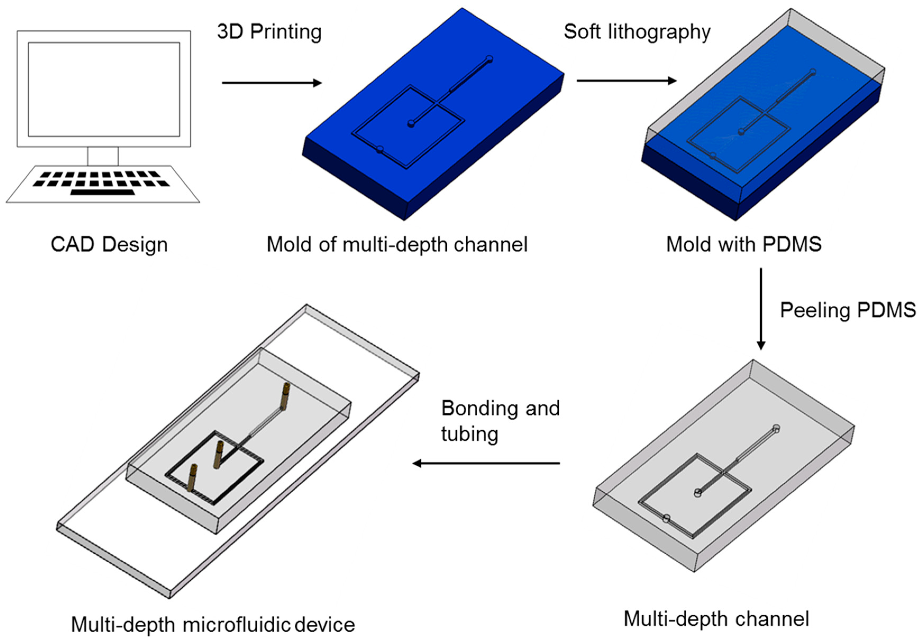
2.2. Microfluidic Device Fabrication

PDMS (Sylgard 184, Dow Corning, Midland, MI, USA) and a curing agent were mixed at the ratio of 10:1. The PDMS mixture was poured into a Petri dish to cover the entire mold. The Petri dish was then placed in a vacuum desiccator for 1 h to remove bubbles inside the mixture. Subsequently, the Petri dish was cured at 70 °C for 4 h. The cured PDMS was peeled off from the mold and washed with isopropanol and ethanol, consecutively, for examination under the SEM or the device bonding process.
To fabricate the microfluidic device, the cured PDMS was punched to have inlets and outlets. The punched channel was then treated with an oxygen plasma (BD-20, Electro-Technic Products, Chicago, IL, USA) for 1 min and bonded onto a plasma-treated glass slide (VWR Scientific, Radnor, PA, USA). The bonding was achieved by placing the microchannel and the glass slide in an oven at 70 °C for 30 min with clamping.

2.3. Microstructure Chracterization

To examine the microstructure of the printed molds, SEM images of the molds coated with a 10 nm thick gold–palladium layer were taken with a field emission SEM system (Mira3 XMU, TESCAN, Brno, Czech Republic, detector: secondary electrons, HV: 20 kV). To examine the microstructures of the peeled PDMS microchannels, the microchannels were also coated with a 10 nm thick gold–palladium layer and then SEM images were taken with the SEM system under the same setting.
In addition to SEM images, the surface profile of 3D printed molds and fabricated PDMS microchannels were characterized using a contact stylus profilometer (Dektak XT, Bruker, Tucson, AZ, USA). The radius of the stylus tip was 2 μm and scanning time was maintained constant at 240 s for all samples.

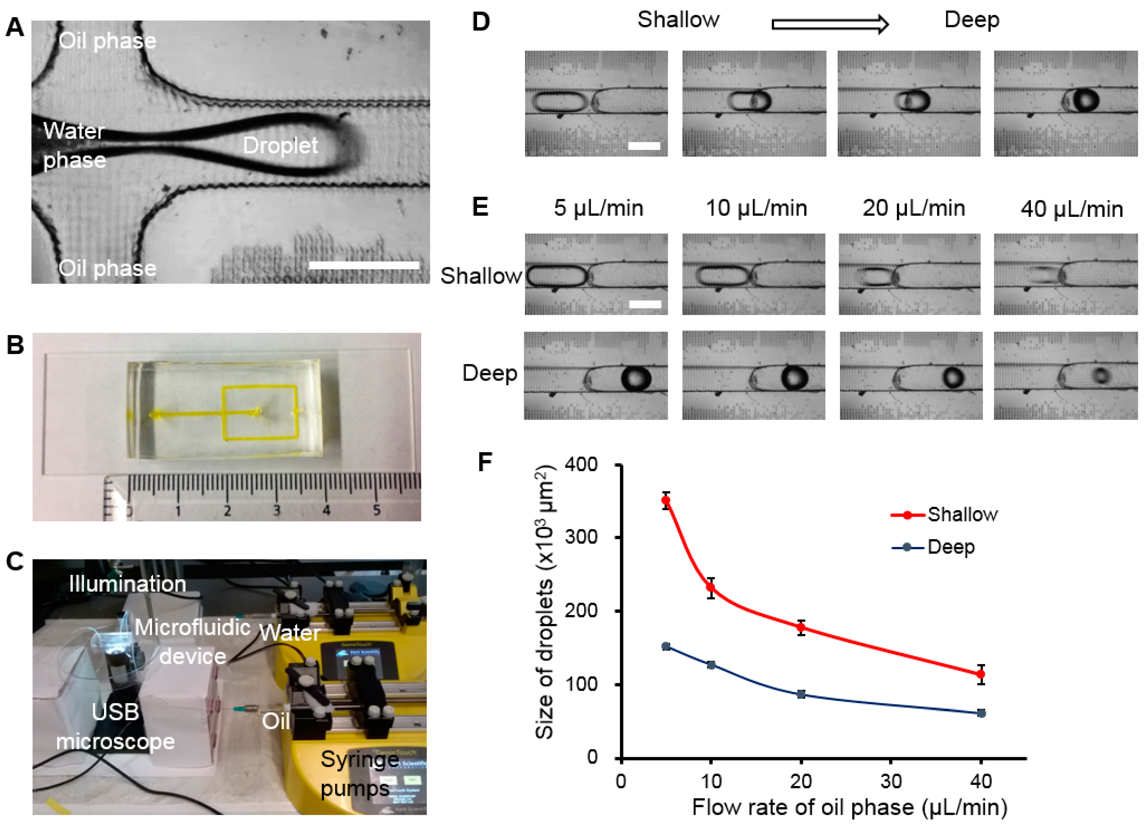
2.4. Droplet Generation

Two solutions were prepared for droplet generation experiments. The RO-water was used as the water phase. The mineral oil (light, high purity, VWR International, Radnor, PA, USA) with 20% v/v Span 80 surfactant (Sigma-Aldrich, St. Louis, MO, USA) was used as the oil phase. The experimental setup was the same as in a previously reported article [26]. Briefly, two syringe pumps (Kent Scientific, Torrington, CT, USA) were used to infuse the water and oil phases at the flow rates of 2 μL/min and 5, 10, 20, or 40 μL/min, respectively. The pumps were connected to a host computer via a USB 2.0 cable. An optical microscope (ToupTek, Hangzhou, China, resolution: 872 × 654, frame rate: 24) was set under the microfluidic device to record video clips of the droplet generation process.
The planar size of droplets was calculated as follows: 1. video clips were exported as a group of frame-based images; 2. representative images of droplets at desired positions were determined manually; and 3. the planar size of droplets in the image was calculated using the built-in measurement function of WCIF ImageJ (University Health Network, Toronto, ON, Canada).

3. Results and Discussion

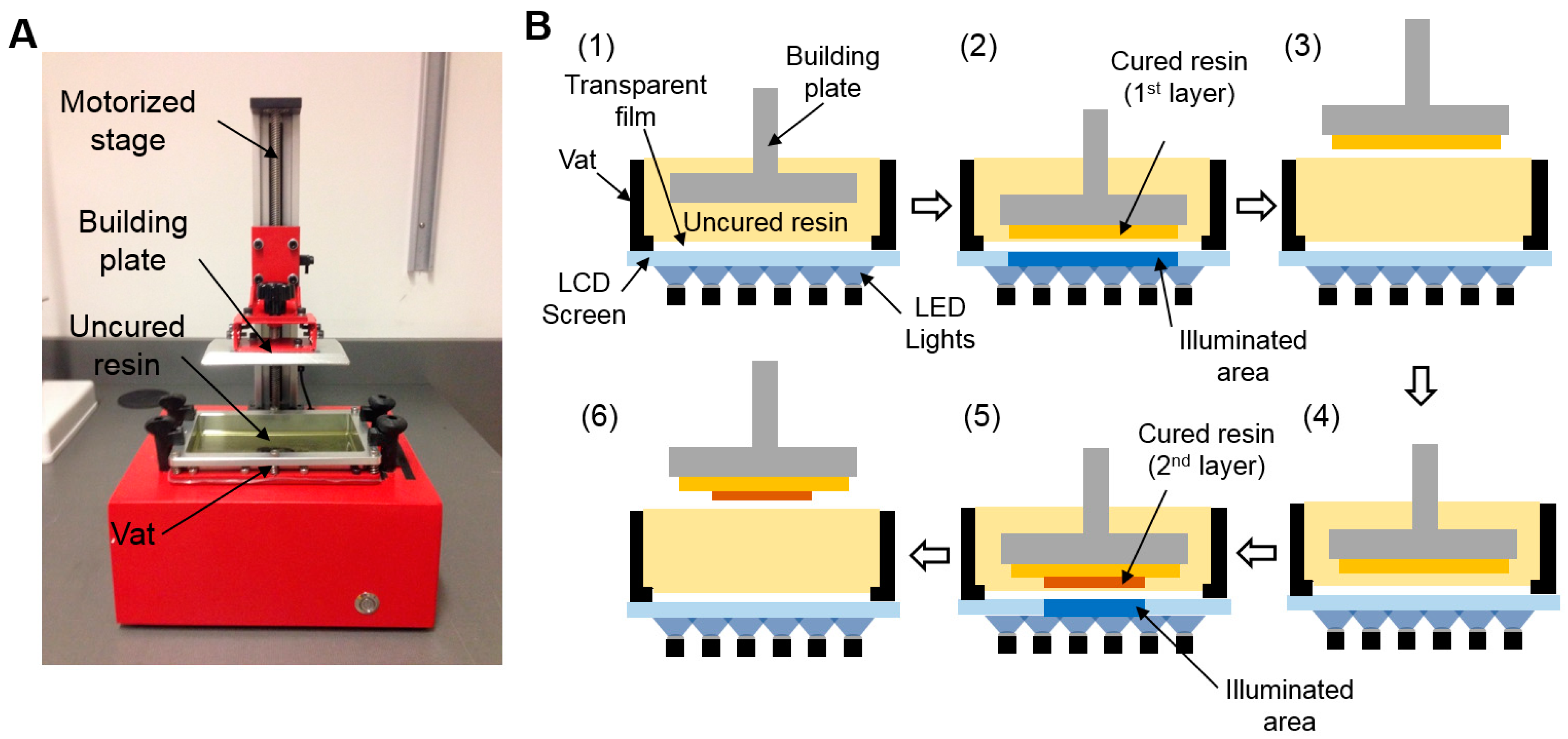
3.1. LCD Stereolithographic Printing

Figure 1A shows the typical structure of an LCD SLA 3D printing system. It contains an LCD screen for projecting sliced images, a vat with non-adhesive treatment for containing uncured resins, and a motorized metal building plate for attaching printed samples. The LCD stereolithographic (SLA) printing is a bottom-up 3D printing method that has several advantages over the top-down digital light processing (DLP) SLA 3D printing system [27]. These include the smaller volume of resin required during fabrication and the capability of achieving a high vertical resolution and a shorter curing time, since the bottom of the resin is sealed from the oxygen-rich environment which inhibits the photocuring process.
The workflow of bottom-up LCD SLA printing is illustrated step-by-step in Figure 1B. Before the printing process, the 3D model (i.e., STL file) was sliced to form a stack of 2D images containing details of an object at a specific layer (i.e., representing the cross-section at a specific layer). At the beginning of printing (Step 1), the building plate moves down to be submerged into the uncured resin. The gap between the building plate and vat is defined by the user as the thickness of the first layer (usually between 50 and 200 μm). Next, the LCD screen is turned on to project the sliced image of the first layer. Only the area designed to be cured is illuminated (Step 2). Depending on the reactivity of the resin and the light intensity of the LCD screen, the curing of one layer is finished within 1 to 60 s. The vat is made from a non-adhesive Teflon film to easily separate the cured resin attached to the bottom of the building plate. Once the curing of the first layer is finished, the building plate moves up to release the printed structure from the vat (Step 3) and moves down to the position where the distance between the bottom of the layer and the vat is to form the user-defined thickness of the second layer (Step 4). Subsequently, patterning the second layer starts (Step 5). Once the second layer is cured, it is integrated to the first layer to form the 3D geometry (Step 6). Steps 4 to 6 are repeated until all slices are subsequently projected and corresponding layers are cured.
It is worth noting that the feature resolution of LCD SLA printing is defined by the pixel resolution of the LCD. The LCD SLA printer uses a 5.5 inch (12.1 cm × 6.8 cm) LCD screen with 2560 × 1440 resolution, giving a pixel size of 47.25 μm. Such high resolution is better than most of the commercially available DLP-based SLA 3D printers (with resolution approximately 100 to 200 μm). The inexpensive LCD SLA printer provides a cost-effective solution for the high-resolution printing.

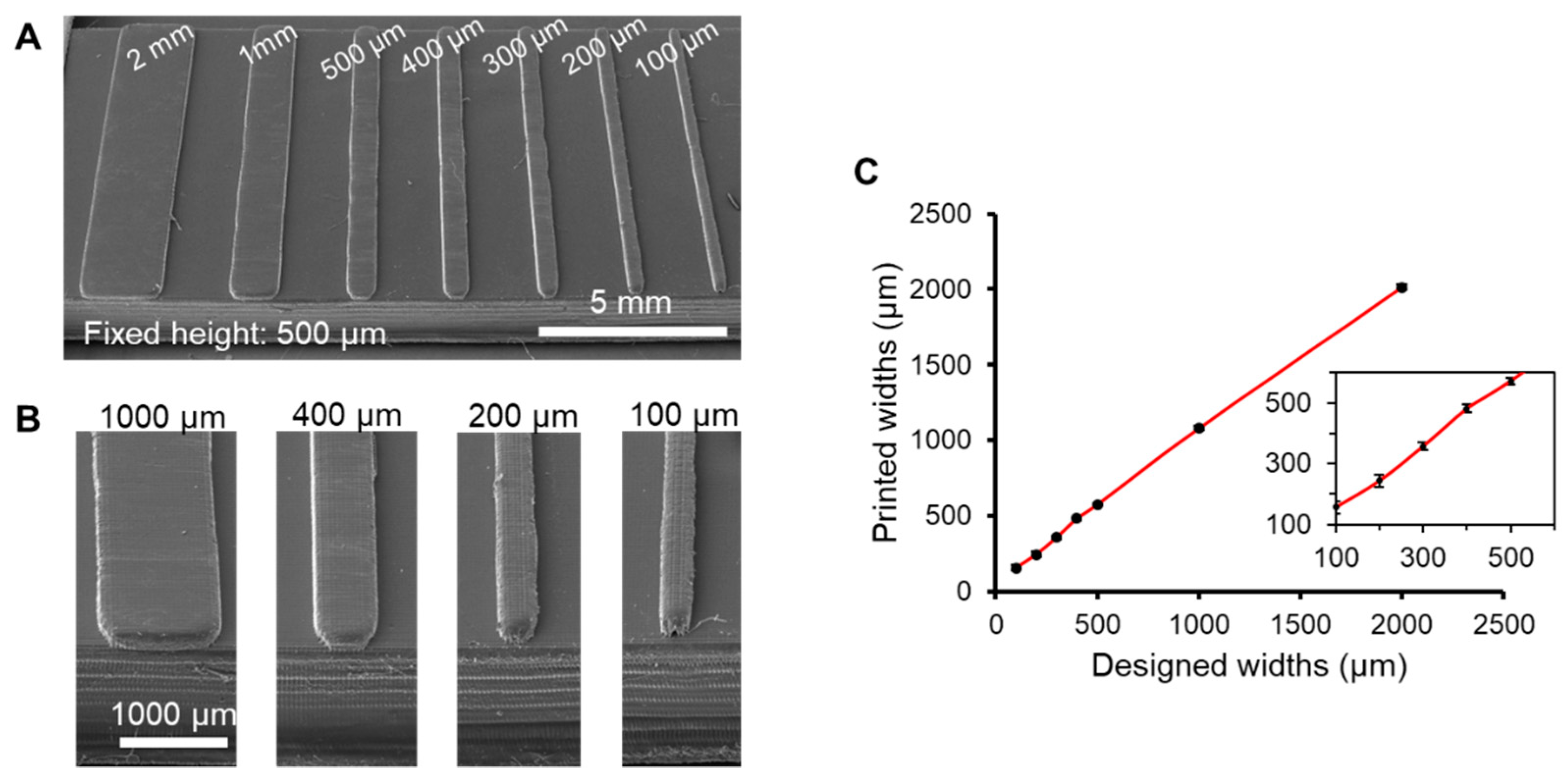
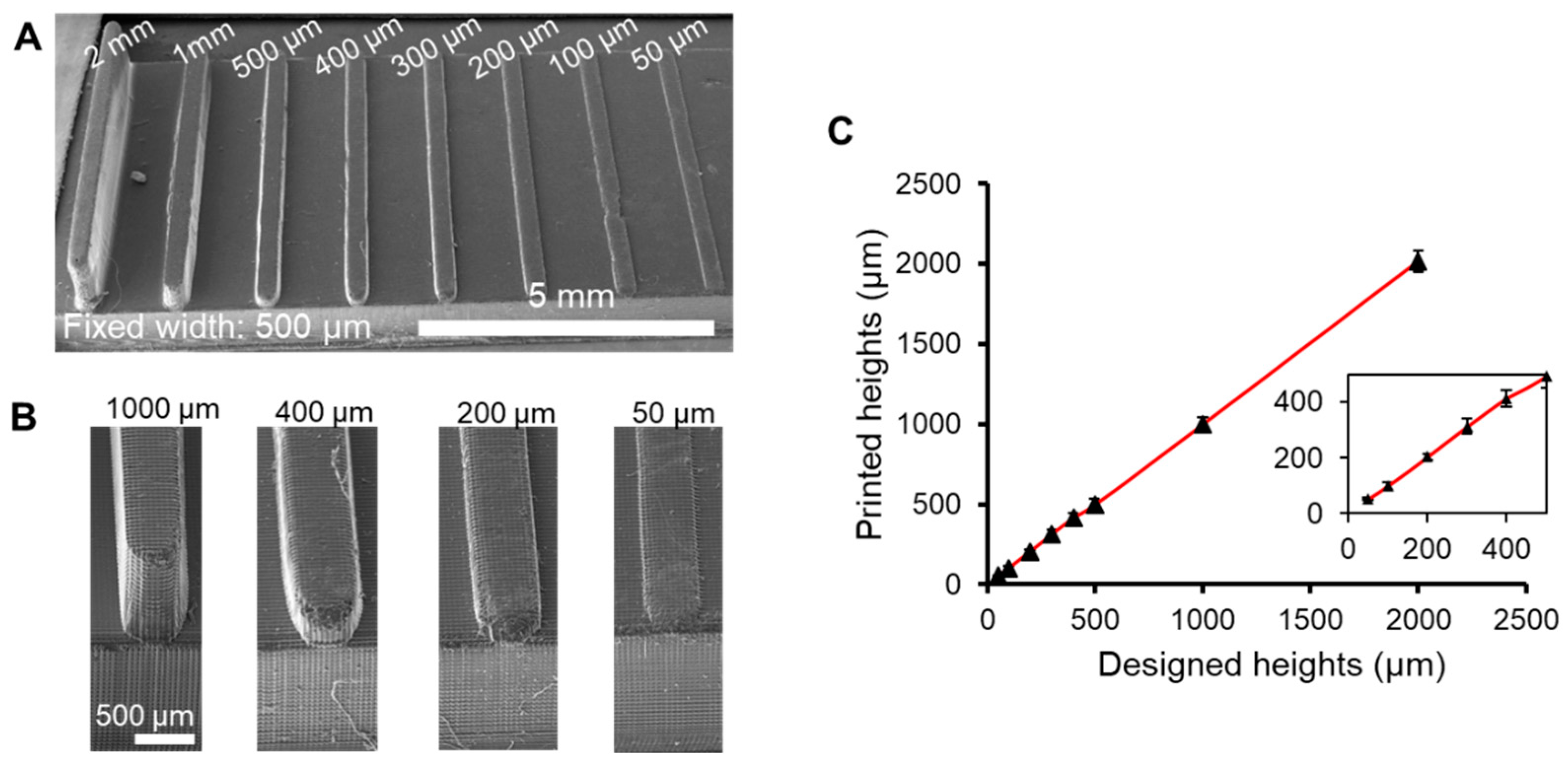
3.2. Characterization of Feature Resolution

We characterized the feature resolution of the printer in the horizontal and vertical directions by printing several line patterns with different widths or heights with the curing time of 15 s for each layer of 50 μm. The entire printing process was done within 20 min. The microstructure of printed objects was examined via an SEM system (Figure 2 and Figure 3). The sample holder was rotated at an angle of 45° to image the vertical face of the samples. Rotating the sample at the given angle resulted in obtaining the projected images of the vertical faces of the sample. Dimensions of the projected images were measured by comparing with the corresponding scale bar on the image and then were used to calculate the actual dimensions of the features using cos(45)·ha (actual height) = hi (imaged height). As can be seen from the SEM images, the line patterns were printed correctly. The smallest visible pattern was 100 μm in the horizontal direction (Figure 2A) and 50 μm in the vertical direction (Figure 3A), respectively. Zoom-in images for different patterns are illustrated (Figure 2B and Figure 3B). For the horizontal features, it was found that the measured width of the designed 100 μm line pattern was around 150 μm. Therefore, the printed sample was slightly overcured. However, the 100 μm line disappeared if the curing time was shorter than 15 s. Therefore, the curing time of 15 s could achieve the minimal feature resolution of 150 μm, although it could result in slight overcuring. We further characterized the line widths of the printed lines (Figure 2C). It was found that, for all the samples, the printed widths were greater than the designed line widths with a constant offset of 50 μm. For the vertical features, unlike the horizontal features, the printed thicknesses were the same as the designed thicknesses (Figure 3C). This was because the thickness of a layer was defined by the gap between the cured layer and the vat rather than the curing time as long as the curing time was long enough to completely cure one layer. In summary, with the 47.25 μm pixel size, the LCD SLA printer could achieve 150 μm positive features in the horizontal direction, which is better than similar studies reported previously [12,13].

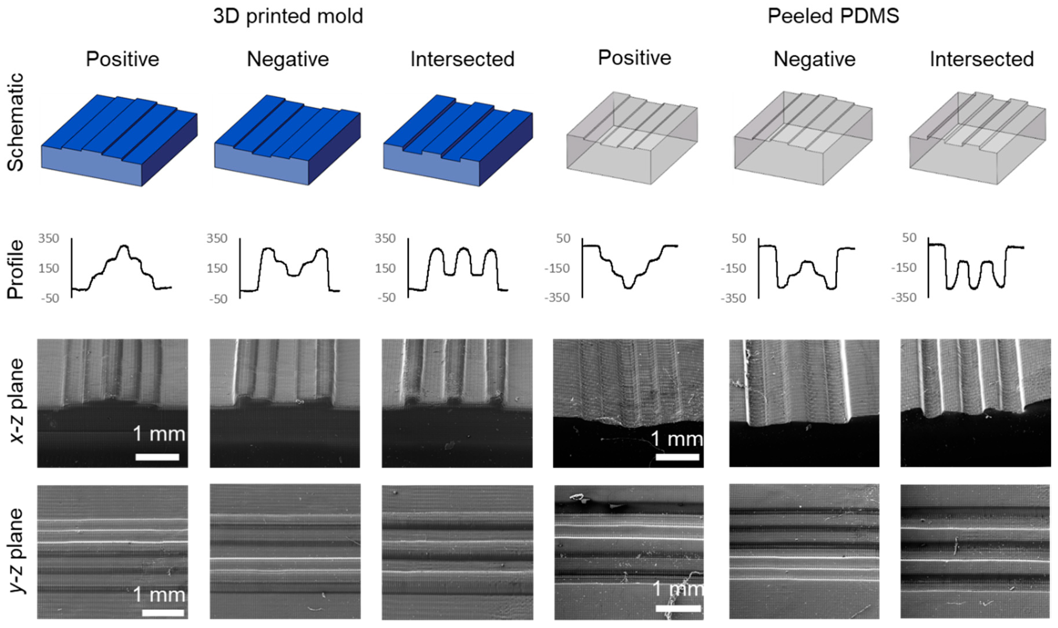
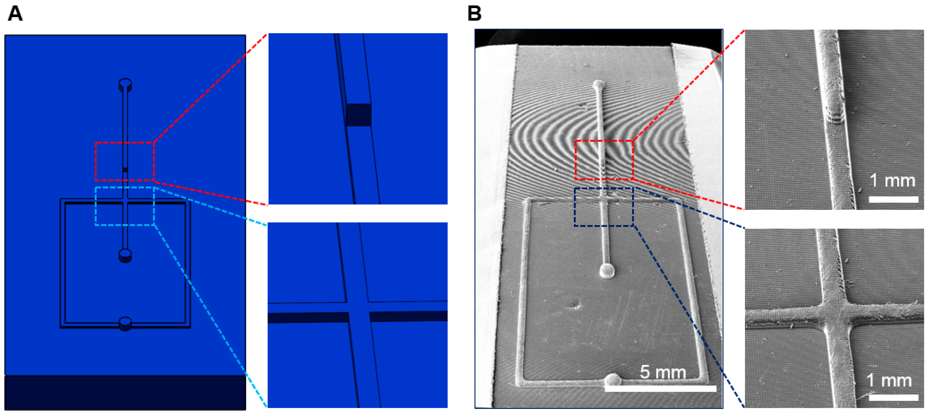
3.3. Fabrication of Multi-Depth Structures

The fabrication flow of the multi-depth channels is shown in Figure 4. First, the positive mold for soft lithography was designed by the computer-aided design software. The designed file was then sliced and printed by the LCD SLA printer to obtain the mold. Soft lithography was then performed by casting the PDMS onto the mold. The cured PDMS with multi-depth channels was peeled off and bonded onto the glass slide via plasma treatment. The whole fabrication process was finished within 6 h.
We designed and fabricated several multi-depth channels (positive, negative, and intersected) and cast PDMS onto them. The widths of all multi-depth channels were fixed at 500 μm. The heights of the positive (100, 200, 300, 200, and 100 μm), negative (300, 200, 100, 200, and 300 μm), and intersected (300, 100, 300, 100, and 300 μm) channels were casted. The microstructure of the printed molds and corresponding PDMS are shown in Figure 5. From the profile measurement data and SEM images, we found that the multi-depth channels could be clearly seen and such features could be transferred to the PDMS properly. Within the field of view (around 4 × 4 mm2), the consistency of the multi-depth channels was good, proving the feasibility of the 3D printing of multi-depth channels for microfluidic applications.
The successful fabrication of multi-depth channels using LCD SLA printing led to the design of a flow-focusing droplet generator with multi-height bumps. Li et al. demonstrated that the bumps can regulate the morphology of droplets [28]. When the droplet moves from the shallow channel to the deep channel, the rod-like compressed droplets are reshaped into spherical balls. The designed flow-focusing device was 400 μm wide and 200 μm high. The bump was 400 μm wide and 600 μm high (Figure 6A). The SEM picture of the 3D printed device is shown in Figure 6B. The multi-depth bump and flow-focusing junction was clearly observed.

3.4. Droplet Generation and Manipulation

Microfabricated droplets can be useful tools in beam manipulation [29], food fabrication [30], and tissue engineering [31]. Precise control over the morphology of droplets has been proven to be an effective way to manipulate light propagation [32] and regulate cell proliferation [33]. Flow-focusing is the most popular design for the microfluidic droplet generation because of its high controllability of droplet size, highly stable generation process, and the ease of device fabrication [34,35]. In a flow-focusing device, droplets are formed when the water phase meets the oil phase at the junction (Figure 7A). When the viscous force of the oil phase overcomes the interfacial forces of the water phase, the water phase starts to break into droplets to minimize its surface tension, according to the Rayleigh instability theory [36]. By changing the flow rates of two phases, the size of the droplets can be controlled accordingly [31].
By casting PDMS on the mold with the bumps, the flow-focusing droplet generator with multi-depth channel was fabricated. The channel is visualized by the yellow food dye (Figure 7B) in which no leakage was observed. Experimental setup established in our previous study [26] was utilized in the droplet generation experiment (Figure 7C). The flow rate of the water phase was fixed at 2 μL/min, whereas the flow rate of the oil phase was changed to regulate the size of droplets. As shown in Figure 7D, a rod-like droplet at the shallow channel became a ball-like droplet once it entered into the deep channel to reduce its surface tension because the deep channel gave more space in the vertical direction to allow it to form a round shape, which agreed well with the previous study [27]. A supporting video showing details of the transition process can be found in the Supplementary Materials. Such a phenomenon was investigated under different flow rates of the oil phase (Figure 7E). The planar size of the droplets, which is the size of the droplets at the focusing plane of the microscope, was quantified using the image processing function provided by ImageJ (Figure 7F). The planar size of the droplets under the flow rate of oil phases at 5, 10, 20, and 40 μL/min was approximately 351 × 103, 232 × 103, 178 × 103, and 113 × 103 μm2 for the shallow channel and 152 × 103, 127 × 103, 87 × 103, and 61 × 103 μm2 for the deep channel, respectively. The planar size of the droplets in the deep channel was approximately half the size of the observed droplets in the shallow channel. The dramatic changes in planar size and the shape (from rod to ball) of droplets indicate that the multi-depth channel is an effective structure to manipulate droplet morphology. Desired size and shape can be well-tuned by changing the flow rate and/or feeding the generated droplet into the channel with different depths.

4. Conclusions

In this paper, an LCD SLA 3D printer was employed for the fabrication of multi-depth microfluidic devices. The 3D printer, benefitting from a higher pixel resolution, can support the feature resolution down to 150 μm in the horizontal direction and 50 μm in the vertical direction, allowing the creation of fine features for various applications. Multi-depth molds with positive, negative, and intersected features were successfully printed. The multi-depth features were transferred to the PDMS for the fabrication of multi-depth microfluidic devices. The successful implementation of the 3D printed multi-depth flow-focusing droplet generator demonstrated the feasibility of using the multi-depth channels to manipulate the morphology and size of the droplets. In summary, LCD SLA 3D printing was found to be an inexpensive and rapid fabrication method for the generation of multi-depth microfluidic devices. Such a technique has a great potential as an alternative method to the multi-depth photolithography, taking into consideration its simplicity, cost effectiveness as well as acceptable resolution.

Supplementary Materials

The following are available online at https://www.mdpi.com/2504-4494/3/1/26/s1.

Author Contributions

Conceptualization, M.G.A.M., Z.W., H.K., and K.K. Methodology, B.M., N.M., and K.K. Investigation, M.G.A.M., Z.W., H.K., and K.K. Formal analysis, Z.W., H.K., and K.K. Visualization, M.G.A.M., B.M., N.M., and K.K. Writing—original draft, Z.W., H.K., and K.K. Writing—review & editing, M.G.A.M., Z.W., H.K., B.M., N.M., and K.K. Funding acquisition, K.K. Supervision, K.K.

Funding

This work was supported by the Natural Sciences and Engineering Research Council of Canada (NSERC) Engage Plus Grant and the Canada Foundation for Innovation John R. Evans Leaders Opportunity Fund.

Acknowledgments

The authors would like to thank David Arkinstall at the UBC Okanagan SEM lab for his assistance in SEM imaging.

Conflicts of Interest

The authors declare no conflict of interest.

References

  1. Berman, B. 3-D printing: The new industrial revolution. Bus. Horiz. 2012, 55, 155–162. [Google Scholar] [CrossRef]
  2. Mandrycky, C.; Wang, Z.; Kim, K.; Kim, D.H. 3D bioprinting for engineering complex tissues. Biotechnol. Adv. 2016, 34, 422–434. [Google Scholar] [CrossRef] [PubMed]
  3. Murphy, S.V.; Atala, A. 3D bioprinting of tissues and organs. Nat. Biotechnol. 2014, 32, 773–785. [Google Scholar] [CrossRef]
  4. Wang, Z.; Sakthivel, K.; Jin, X.; Kim, K. 3D bioprinting composite tissue. 3D Biopr. Reconstr. Surg. Tech. Appl. 2017, 393–412. [Google Scholar] [CrossRef]
  5. Kang, H.-W.; Lee, S.J.; Ko, I.K.; Kengla, C.; Yoo, J.J.; Atala, A. A 3D bioprinting system to produce human-scale tissue constructs with structural integrity. Nat. Biotechnol. 2016, 34, 312–319. [Google Scholar] [CrossRef] [PubMed]
  6. Waheed, S.; Cabot, J.M.; Macdonald, N.P.; Lewis, T.; Guijt, R.M.; Paull, B.; Breadmore, M.C. 3D printed microfluidic devices: Enablers and barriers. Lab Chip 2016, 16, 1993–2013. [Google Scholar] [CrossRef]
  7. Bonyár, A.; Sántha, H.; Ring, B.; Varga, M.; Kovács, J.G.; Harsányi, G. 3D Rapid Prototyping Technology (RPT) as a powerful tool in microfluidic development. Procedia Eng. 2010, 5, 291–294. [Google Scholar] [CrossRef] [Green Version]
  8. Au, A.K.; Huynh, W.; Horowitz, L.F.; Folch, A. 3D-Printed Microfluidics. Angew. Chem. Int. Ed. 2016, 55, 3862–3881. [Google Scholar] [CrossRef]
  9. Wu, J.; Gu, M. Microfluidic sensing: State of the art fabrication and detection techniques. J. Biomed. Opt. 2011, 16, 080901. [Google Scholar] [CrossRef] [PubMed]
  10. Wang, Z.; Samanipour, R.; Koo, K.; Kim, K. Organ-on-a-Chip Platforms for Drug Delivery and Cell Characterization: A Review. Sens. Mater. 2015, 27, 487–506. [Google Scholar]
  11. Anderson, K.B.; Lockwood, S.Y.; Martin, R.S.; Spence, D.M. A 3D printed fluidic device that enables integrated features. Anal. Chem. 2013, 85, 5622–5626. [Google Scholar] [CrossRef] [PubMed]
  12. Shallan, A.I.; Smejkal, P.; Corban, M.; Guijt, R.M.; Breadmore, M.C. Cost-effective three-dimensional printing of visibly transparent microchips within minutes. Anal. Chem. 2014, 86, 3124–3130. [Google Scholar] [CrossRef] [PubMed]
  13. Wang, Z.; Martin, N.; Hini, D.; Mills, B.; Kim, K. Rapid Fabrication of Multi-layer Microfluidic Devices using Liquid Crystal Display-based Stereolithography 3D Printing System. 3D Print. Addit. Manuf. 2017, 4, 156–164. [Google Scholar] [CrossRef]
  14. Gong, H.; Woolley, A.T.; Nordin, G.P. 3D printed high density, reversible, chip-to-chip microfluidic interconnects. Lab Chip 2018, 18, 639–647. [Google Scholar] [CrossRef]
  15. Rogers, C.I.; Qaderi, K.; Woolley, A.T.; Nordin, G.P. 3D printed microfluidic devices with integrated valves. Biomicrofluidics 2015, 9, 016501. [Google Scholar] [CrossRef] [Green Version]
  16. Hampson, S.M.; Rowe, W.; Christie, S.D.R.; Platt, M. 3D printed microfluidic device with integrated optical sensing for particle analysis. Sens. Actuators B Chem. 2018, 256, 1030–1037. [Google Scholar] [CrossRef]
  17. Hwang, Y.; Paydar, O.H.; Candler, R.N. 3D printed molds for non-planar PDMS microfluidic channels. Sens. Actuators A Phys. 2015, 226, 137–142. [Google Scholar] [CrossRef]
  18. Wang, Z.; Samanipour, R.; Kim, K. The cleanroom-free rapid fabrication of a liquid conductivity sensor for surface water quality monitoring. Microsyst. Technol. 2016, 22, 2273–2278. [Google Scholar] [CrossRef]
  19. Hwang, Y.; Seo, D.; Roy, M.; Han, E.; Candler, R.N.; Seo, S. Capillary Flow in PDMS cyclindrical Microfluidic Channel Using 3-D Printed Mold. J. Microelectromech. Syst. 2016, 25, 238–240. [Google Scholar] [CrossRef]
  20. Walczak, R.; Adamski, K. Inkjet 3D printing of microfluidic structures—On the selection of the printer towards printing your own microfluidic chips. J. Micromech. Microeng. 2015, 25, 085013. [Google Scholar] [CrossRef]
  21. Anderson, J.R.; Chiu, D.T.; Jackman, R.J.; Chemiavskaya, O.; McDonald, J.C.; Wu, H.; Whitesides, S.H.; Whitesides, G.M. Fabrication of topologically complex three-dimensional microfluidic systems in PDMS by rapid prototyping. Anal. Chem. 2000, 72, 3158–3164. [Google Scholar] [CrossRef] [PubMed]
  22. Thorsen, T.; Maerkl, S.J.; Quake, S.R. Microfluidic Large-Scale Integration. Science 2002, 298, 580–584. [Google Scholar] [CrossRef] [Green Version]
  23. Mata, A.; Fleischman, A.J.; Roy, S. Fabrication of multi-layer SU-8 microstructures. J. Micromech. Microeng. 2006, 16, 276–284. [Google Scholar] [CrossRef]
  24. Zhang, M.; Wu, J.; Wang, L.; Xiao, K.; Wen, W. A simple method for fabricating multi-layer PDMS structures for 3D microfluidic chips. Lab Chip 2010, 10, 1199. [Google Scholar] [CrossRef]
  25. Li, X.; Yu, Z.T.F.; Geraldo, D.; Weng, S.; Alve, N.; Dun, W.; Kini, A.; Patel, K.; Shu, R.; Zhang, F.; et al. Desktop aligner for fabrication of multilayer microfluidic devices. Rev. Sci. Instrum. 2015, 86, 075008. [Google Scholar] [CrossRef] [Green Version]
  26. Wang, Z.; Samanipour, R.; Gamaleldin, M.; Sakthivel, K.; Kim, K. An automated system for high-throughput generation and optimization of microdroplets. Biomicrofluidics 2016, 10, 054110. [Google Scholar] [CrossRef] [Green Version]
  27. Pan, Y.; Zhou, C.; Chen, Y. Rapid Manufacturing in Minutes: The Development of a Mask Projection Stereolithography Process for High-Speed Fabrication. J. Manuf. Sci. Eng. 2012, 134, 405–414. [Google Scholar] [CrossRef]
  28. Li, H.; Fan, Y.; Conchouso, D.; Foulds, I.G. CO2 laser-induced bump formation and growth on polystyrene for multi-depth soft lithography molds. J. Micromech. Microeng. 2012, 22, 115037. [Google Scholar] [CrossRef]
  29. Jin, X.; Guerrero, D.; Klukas, R.; Holzman, J.F. Microlenses with tuned focal characteristics for optical wireless imaging. Appl. Phys. Lett. 2014, 105, 031102. [Google Scholar] [CrossRef]
  30. Guzey, D.; McClements, D.J. Formation, stability and properties of multilayer emulsions for application in the food industry. Adv. Colloid Interface Sci. 2006, 128, 227–248. [Google Scholar] [CrossRef]
  31. Samanipour, R.; Wang, Z.; Ahmadi, A.; Kim, K. Experimental and computational study of microfluidic flow-focusing generation of gelatin methacrylate hydrogel droplets. J. Appl. Polym. Sci. 2016, 133. [Google Scholar] [CrossRef]
  32. Born, B.; Landry, E.L.; Holzman, J.F. Electrodispensing of Microspheroids for Lateral Refractive and Reflective Photonic Elements. IEEE Photonics J. 2010, 2, 873–883. [Google Scholar] [CrossRef]
  33. Clausell-Tormos, J.; Lieber, D.; Baret, J.C.; El-Harrak, A.; Miller, O.J.; Frenz, L.; Blouwolff, J.; Humphry, K.J.; Köster, S.; Duan, H.; et al. Droplet-Based Microfluidic Platforms for the Encapsulation and Screening of Mammalian Cells and Multicellular Organisms. Chem. Biol. 2008, 15, 427–437. [Google Scholar] [CrossRef] [Green Version]
  34. Anna, S.L.; Bontoux, N.; Stone, H.A. Formation of dispersions using “flow focusing” in microchannels. Appl. Phys. Lett. 2003, 82, 364–366. [Google Scholar] [CrossRef]
  35. Takeuchi, S.; Garstecki, P.; Weibel, D.B.; Whitesides, G.M. An axisymmetric flow-focusing microfluidic device. Adv. Mater. 2005, 17, 1067–1072. [Google Scholar] [CrossRef]
  36. Strutt, J.W.; Rayleigh, L. On the Instability of Jets. Proc. London Math. Soc. 1878, 1, 4–13. [Google Scholar]
Figure 1. Liquid crystal display (LCD) stereolithographic (SLA) three-dimensional (3D) printing system and working principle. (A) Photograph of a custom-built LCD SLA 3D printer. (B) Step-by-step workflow of the LCD SLA 3D printer.
Jmmp 03 00026 g001
Figure 2. Characterization of the feature resolution in the horizontal direction. (A) SEM images of the line patterns printed for characterization. The heights of the patterns were fixed at 500 μm. The value above each line indicates the designed widths of the specific line. (B) Zoom-in images of the line patterns with the designed widths of 1000, 400, 200, and 100 μm. (C) Relationship between designed widths and printed widths. The printed width is slightly greater than the designed one due to the overcuring.
Jmmp 03 00026 g002
Figure 3. Characterization of feature resolution in the vertical direction. (A) SEM images of the line patterns printed for characterization. The widths of the patterns were fixed at 500 μm. (B) The zoom-in images of the line patterns with the designed heights of 1000, 400, 200, and 100 μm. (C) Relationship between designed heights and printed heights. The printed heights are almost same as the designed one and not affected by the overcuring.
Jmmp 03 00026 g003
Figure 4. Fabrication flow of a multi-depth microfluidic device using LCD SLA 3D printing.
Jmmp 03 00026 g004
Figure 5. Surface profile data and SEM images of the 3D printed mold and corresponding polydimethylsiloxane (PDMS) patterns with multi-depth features.
Jmmp 03 00026 g005
Figure 6. Mold design and fabrication of the flow-focusing droplet generator with multi-depth features. (A) Solid model of the mold for printing. (B) SEM pictures of the printed mold. Zoom-in images show the details of the multi-depth channel and the flow-focusing junction.
Jmmp 03 00026 g006
Figure 7. Droplet generation and manipulation using the multi-depth microfluidic device. (A) A microscope image shows the flow-focusing junction for droplet generation. Scale bar = 500 μm. (B) A photograph of the fabricated multi-depth microfluidic device. The channel is visualized by the yellow food dye. (C) Experimental setup of the droplet generation. Water and oil phases were infused to the flow-focusing junction using the syringe pumps. (D) The time-lapse image to show the morphology and size changes of droplets (flow rate of oil phase: 10 μL/min and time lapse between two nearby images: 41 ms). Scale bar = 500 μm. (E) Morphologies of different sizes of droplets before and after entering the deep channel. Scale bar = 500 μm. (F) Quantification of planar size of droplets before and after entering the deep channel (n = 5).
Jmmp 03 00026 g007

