1. Introduction
Silicon (Si) technology has been well advanced to develop complex micro-electro-mechanical systems (MEMS) consisting of various functional units including structural parts, elastic components, as well as sensors and microactuators based on electrostatics, magnetomotive or electrothermal principles, see e.g., [
1,
2,
3]. Despite this versatility, current microactuation concepts exhibit a number of limitations, including low power efficiency, limitations of downscaling, and technology constraints, which become even more severe upon further downscaling to nanometer dimensions. Shape Memory Alloy (SMA)-based actuators may overcome these constraints due to their large work density of up to 10
7 Jm⁻
3 and favorable downscaling behavior [
4].
The monolithic integration of SMA actuators with active and passive Si structures enables various MEMS applications, including switching and tuning functions for mechanics and photonics [
5,
6]. The development of combined Si MEMS and SMA microactuator systems requires monolithic integration of SMA films compatible with MEMS fabrication processes. In recent years, monolithic fabrication as well as hybrid integration processes have been successfully demonstrated, allowing for parallel fabrication of SMA film actuators on the wafer scale [
7,
8,
9]. Major challenges are the high annealing temperature (minimum 500 °C) and thermo-mechanical treatment required for SMA microactuator fabrication, which may cause interdiffusion, delamination, and process incompatibilities with other MEMS components [
4]. Sputtered NiMnGa and TiNiHf SMA films are especially interesting for use in micro- and nanoactuators due to tunable phase transformation temperatures, tunable hysteresis, and decent functional fatigue properties [
8,
9,
10,
11].
SMA actuators being thermal actuators require either a direct or an indirect heating mechanism. Direct Joule heating can be implemented, in principle, down to nanometer dimensions, as it does not require any additional structures such as microheaters. However, direct Joule heating of SMA actuators consisting of beam cantilevers with decreasing dimensions results in an increasing temperature gradient along the beam length that can well exceed 50 K/µm [
12]. As a result, the SMA layer undergoes phase transformation only in a local region, which results in a negligible contribution of the shape memory effect to the deflection characteristics [
12].
In this study, we present a process for the co-integration of SMA and Si microstructures focusing on NiMnGa and NiTi(Hf) films to enable SMA/Si bimorph microactuation and introduce an approach to optimize the bimorph actuator layout with respect to temperature gradient in order to maximize deflection and to minimize power consumption.
2. Fabrication of SMA-Si Bimorph Layer
The process flow under investigation for the fabrication of SMA/Si bimorph microactuators is shown schematically in
Figure 1. Double beam cantilevers are chosen for actuator layout to enable electro-thermal actuation by Joule heating. Silicon-On-Insulator (SOI) wafers with Si device layer thickness of 2 µm are chosen as the starting substrate for co-integration. SMA-based films are deposited by magnetron sputtering with a thickness of several microns along with a top layer of Au. Amorphous SMA films are then crystallized at selected temperatures (500–700°C). First, the pattern is transferred to the Au layer by ultra-high-resolution electron beam lithography (EBL) and wet-etching of Au. Second, the thick SMA films are wet etched by hydrofluoric acid (HF) and nitric acid (HNO
3) solution, while thin films are dry-etched by reactive ion beam etching (RIBE). Third, the Si device layer is structured by reactive ion etching (RIE) using the cryo process. Finally, freestanding SMA/Si bimorph cantilevers are obtained by wet etching of the buried silicon oxide using hydrofluoric acid. This process flow is compatible with fabricating co-integrated SMA/Si bimorph and micromechanical structures.
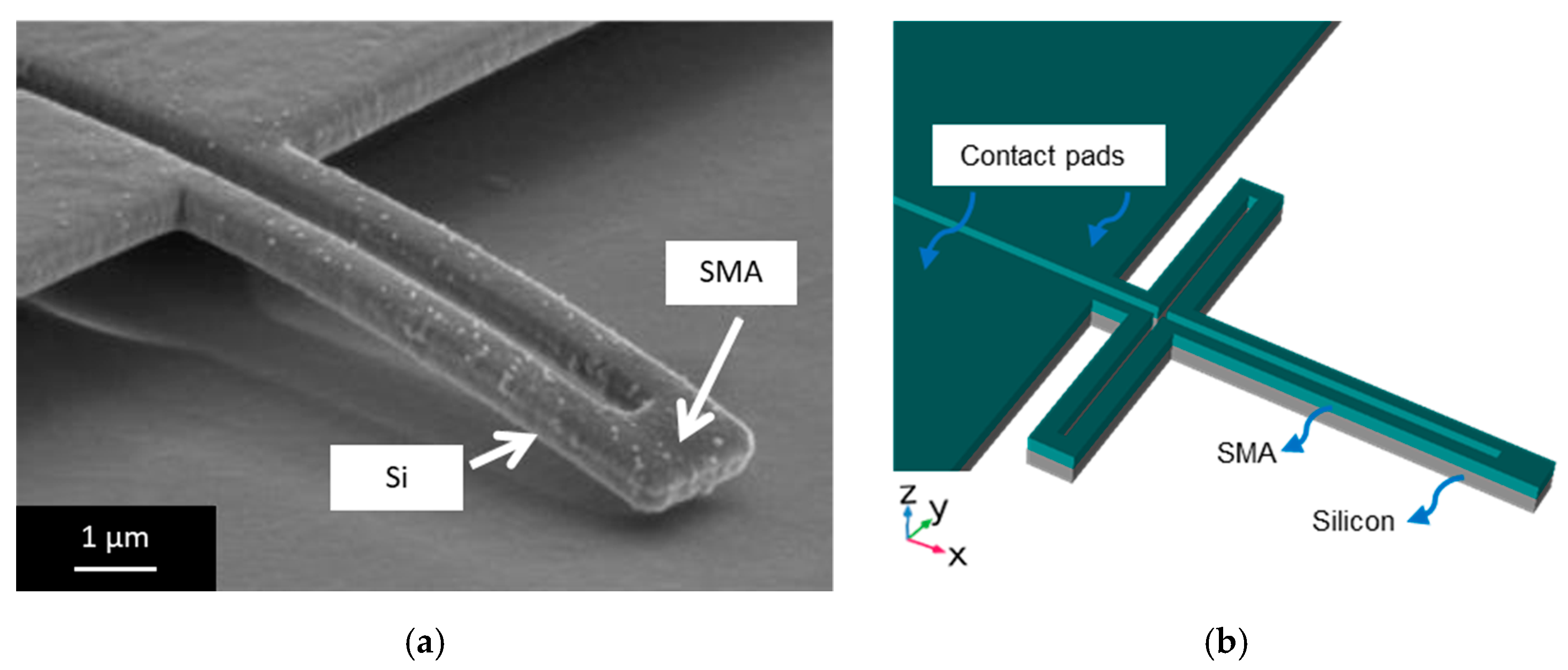
Figure 2a shows a scanning electron micrograph of a typical freestanding SMA/Si double-beam cantilever with a non-optimized layout. The SMA and Si layers of the bimorph device can be distinguished clearly.
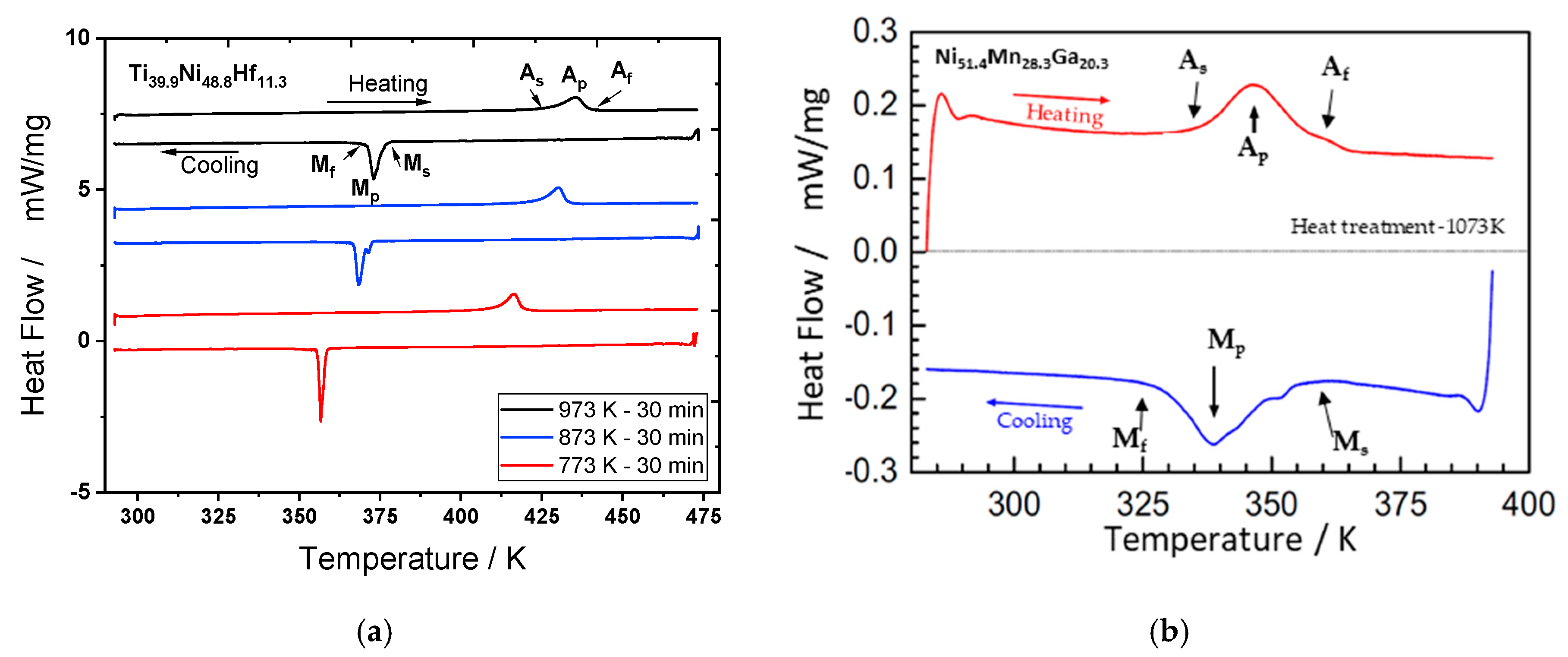
3. SMA Film Properties
Energy dispersive x-ray spectroscopy (EDX) measurements show an average film composition of Ti
38.9Ni
48.8Hf
11.3 for sputtered amorphous TiNiHf films. Since the films are sputtered in the amorphous state, it is possible to adjust the SMA transformation temperatures (i.e., actuator operation temperatures) via the annealing temperature. The Differential Scanning Calorimetry (DSC) measurements shown in
Figure 2a confirm that as the TiNiHf alloy annealing temperature increases, the transformation temperatures also increase. The latent heat, thermal hysteresis width, and transformation temperatures of the films annealed at 773 K, 873 K and 973 K for 30 min are given in
Table 1 together with the phase transformation temperatures of a NiMnGa film.
Figure 2b shows a DSC characteristic of the polycrystalline NiMnGa film, which has been heat-treated at 1073 K. The chemical composition of the film has been determined by the inductive coupled plasma method to be Ni
51.4Mn
28.3Ga
20.3.
4. Modelling Approach
A Finite Element Model (FEM) for mechanical and thermal analyses is developed and implemented using COMSOL Multiphysics 5.5. The Electric-Current module, Heat-Transfer module and Structural-Mechanics module are coupled together to implement a Joule heating-based deflection model of the SMA/Si bimorph devices. The resistive heating due to electro-thermal coupling acts as a thermal load for the Solid-Mechanics interface, causing differential thermal expansion as well as deformation due to martensitic phase transformation.
The shape memory effect is described by the Tanaka-type model, in which the martensite volume fraction
is introduced which approximates the phase transformation by an exponential step function that varies between 1 (martensite state) and 0 (austenite state) depending on temperature and stress. In this phase transformation regime, the temperature-dependent material properties are defined by a simple rule of mixture, which introduces two independent parameter sets describing the martensite and austenite state. For example, the electrical conductivity
of SMA is approximated as a mixture of electrical conductivity in austenite phase
and in martensite phase
,
Our approach for design optimization is to provide additional folded beam structures (wings) at the onset of the double-beam cantilever in a perpendicular direction as illustrated in
Figure 3b. In this case, the wing width, wing length, and the number of folds (overall path length) of the additional structures are the major design parameters for tuning the temperature gradient resulting from Joule heating.
Table 2 summarizes the material parameters of Si and two different SMA materials (NiMnGa and NiTi) used in the simulations. The key material parameters for resistive Joule heating are electrical conductivity
and thermal conductivity κ. The thermal conductivity of SMA is approximated by the Wiedemann-Franz law [
13] describing the heat conductivity
as a function of electrical conductivity
,
with the proportionality constant
[
13]. The thermal conductivity of Si [
14] is approximated by,
For the mechanical response, the necessary input parameters are Young’s modulus (E), Poisson ratio (ν), and the thermal expansion coefficient (α). In the phase transformation regime, the stress and the coefficient of thermal expansion (CTE) values are approximated by the rule of mixture as described before.
5. Homogenization of Temperature Profiles
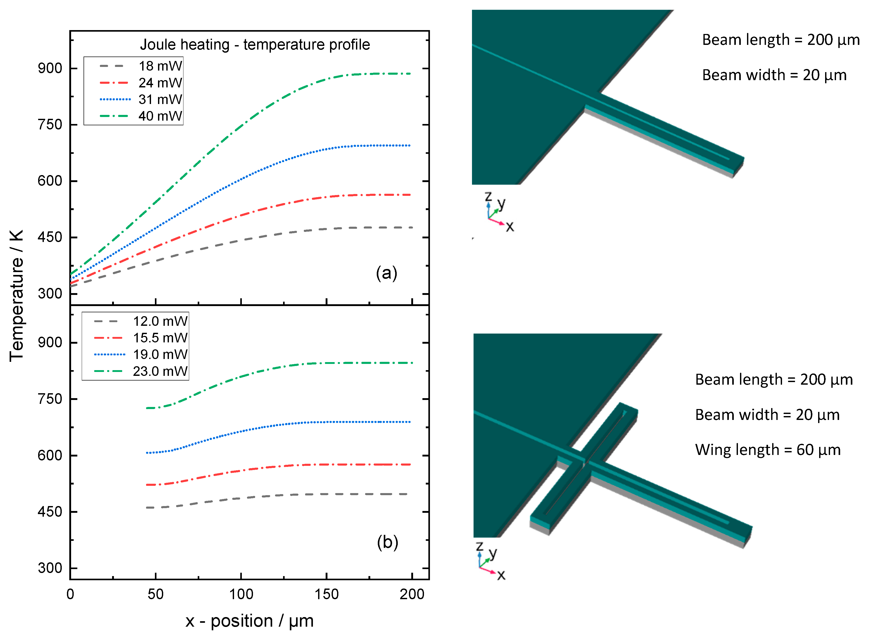
Figure 4 shows a series of simulated temperature profiles of a NiMnGa/Si bimorph actuator for different values of electrical power. A standard double-beam cantilever design (denoted as non-optimized design in the following) and a temperature-homogenized design with additional folded beam structure is considered with 20 μm beam width and 200 μm beam length. The width and length of the folded structures are 20 and 60 μm, respectively. In a first approach, a constant layer thickness of 2 μm is considered for both SMA and Si layers. The x-position corresponds to the path along the beam length.
Figure 4a reveals that very high temperatures occur at the beam tips, while the onset of the beams is close to room temperature. At an electrical power of 40 mW, the maximum temperature at the beam tip reaches 900 K, while the beam onset has a temperature of 350 K. As a result, a larger electric power is required to heat the entire structure, causing heat accumulation at the beam tip. Furthermore, for increasing electrical heating power, the temperature gradients along the beam lengths are increasing.
Figure 4b shows temperature profiles of the temperature-homogenized design. Behind the wing structure (x > 50 µm), almost homogeneous temperature profiles occur along the beam in contrast to non-optimized cantilever structures. The homogeneous temperature profiles eliminate the issue of different phase states at local regions of the cantilevers and, thus, allow for complete phase transformation.
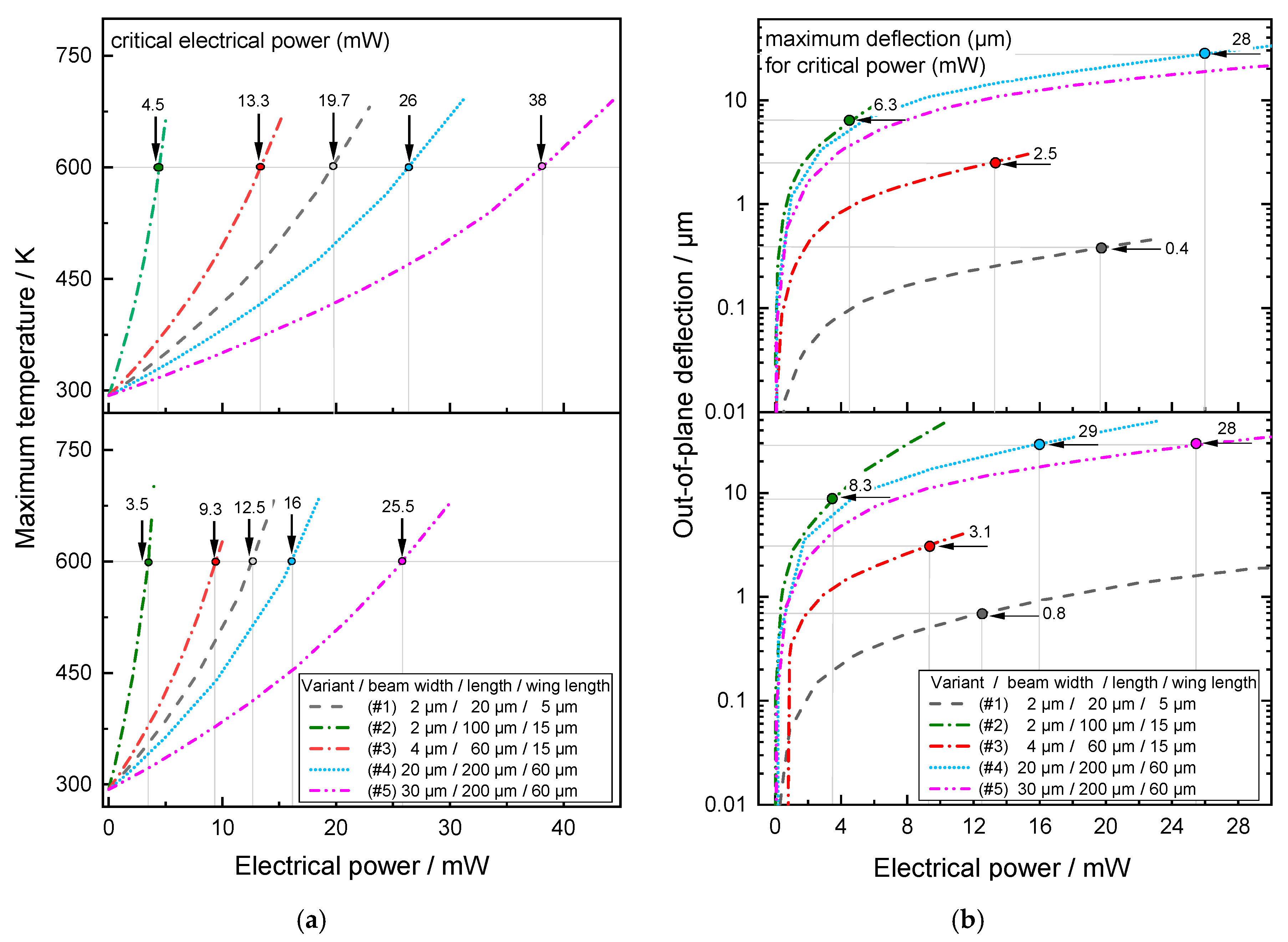
6. Evaluation of Critical Electrical Power and Maximum Deflection
At typical heat-treatment temperatures between 600 K and 800 K, interdiffusion occurs and, consequently, shape memory properties deteriorate. Therefore, a critical temperature of 600 K is considered here as the operational limit of the actuator device.
Figure 5a shows simulated characteristics of maximum temperature at the beam tip as a function of electrical heating power for different geometries of non-optimized and temperature-homogenized cantilevers. The critical electrical power limits of reaching the critical temperature of 600 K are indicated for both cases. The heating is maximum at the beam tip, so the beam tip is taken as the measurement point. The source of heat is characterized by the given electrical power. Therefore, the operational power limit is also calculated from this critical temperature, as indicated in
Figure 5a. For a study on the dependencies of beam geometry, a set of different NiMnGa/Si bimorph variants is selected featuring beam widths and lengths up to 30 μm and 200 μm (see
Table 3).
Comparing variants #1 and #4, the width and length are upscaled by a factor of 10 while keeping the width-to-length ratio constant (w/l aspect ratio of 10). The critical electrical power for variants #1 and #4 for the non-homogenized model is 19.7 mW and 26 mW, respectively. In the case of the temperature-homogenized model, this critical power limit decreases to 16 mW and 12.5 mW, which corresponds to a 35 % reduction in power consumption. Comparing variants #4 and #5 in
Figure 5a, a huge difference of 40 % in critical power is observed, resulting from the variation of beam width. In the case of 100 μm beam length, both models reveal the lowest values of critical power of 4.5 mW (non-optimized) and 3.5 mW (temperature-homogenized), respectively. In all cases, temperature-homogenized designs reveal lower electrical power to achieve comparable maximum temperatures.
Simulated characteristics of out-of-plane deflection at the beam tip are shown in
Figure 5b as a function of electrical heating power. The maximum achievable deflections are indicated corresponding to the critical electrical power limits. Comparing variant #1 of both the non-optimized and temperature-homogenized designs, the deflection increases by a factor of 2, and power consumption reduces by more than 35 %. In general, for bimorphs, the thickness of SMA/Si layers and the length of the cantilever defines the out-of-plane deflection, whereas the beam width has no contribution to it. This is observed by comparing variants #4 and #5, where the deflection is merely the same for both non-homogenized and homogenized models. However, a significant reduction in the critical power limit by 30–40% is present. This implies that the range of power limit can be changed without compromising the deflection, depending on the design requirements.
7. Conclusions
This study presents an approach to fabricate SMA/Si bimorph microactuators with cantilever beam design and to homogenize their temperature profile caused by Joule heating. The focus is on NiMnGa and NiTi(Hf) films with tunable phase transformation temperatures. By introducing folded beam structures perpendicular to the cantilever structures, the temperature profiles are homogenized, allowing for uniform phase transformation. Critical electrical power values are determined for different geometric variants indicating the operational limit of the SMA/Si bimorph microactuators. By temperature homogenization, we could reduce power consumption by up to 35%. Upscaling the temperature-homogenized geometry without changing the aspect ratio w/l allows for reduction in electrical heating power by 30-40%. The maximum deflection is increased by a factor of 2 for the smallest cantilever design under investigation with beam width/length of 2/20 µm.
Author Contributions
M.K., and E.Q. developed the concept; G.A. developed the simulation model, performed the simulations and experiments, analyzed the data and wrote the draft of the manuscript; Z.L. contributed to experiments and data analysis; S.C. designed the TiNiHf experiments and analyzed the data; P.V. contributed to SMA sample preparation; M.K. supervised the work, reviewed and edited the manuscript. All authors have read and agreed to the published version of the manuscript.
Acknowledgments
This research has received funding from the German Research Foundation (DFG) within the priority program “SPP2206–Cooperative Multistage Multistable Microactuator Systems”. Further, we would like to thank Duygu Dengiz for supporting us with EDX measurements.
Conflicts of Interest
The authors declare no conflict of interest.
Abbreviations
The following abbreviations are used in this manuscript:
| EBL | Electron Beam Lithography |
| EDX | Energy dispersive x-ray spectroscopy |
| CTE | Coefficient of Thermal Expansion |
| DSC | Differential Scanning Calorimetry |
| FEM | Finite Element Modeling |
| MEMS | Micro-Electro-Mechanical Systems |
| RIBE | Reactive Ion Beam Etching |
| SMA | Shape Memory Alloy |
| SOI | Silicon-On-Insulator |
References
- Hollar, S.; Bergbreiter, S.; Pister, K. Bidirectional inchworm motors and two-DOF robot leg operation. In Proceedings of the TRANSDUCERS ’03. 12th International Conference on Solid-State Sensors, Actuators and Microsystems, Boston, MA, USA, 8–12 June 2004. Digest of Technical Papers (Cat. No.03TH8664). [Google Scholar]
- Last, M.; Subramaniam, V.; Pister, K. Out of plane motion of assembled microstructures using a single-mask SOI process. In Proceedings of the 13th International Conference on Solid-State Sensors, Actuators and Microsystems, TRANSDUCERS ’05, Seoul, Korea, 22 August 2005. Digest of Technical Papers. [Google Scholar]
- Yeh, R.; Hollar, S.; Pister, K. Single mask, large force, and large displacement electrostatic linear inchworm motors. J. Microelectromech. Syst. 2002, 11, 330–336. [Google Scholar] [CrossRef]
- Kohl, M. Shape Memory Microactuators; Springer: Berlin/Heidelberg, Germany, 2004. [Google Scholar]
- Lambrecht, F.; Aseguinolaza, I.; Chernenko, V.; Kohl, M. Integrated SMA-based NEMS actuator for optical switching. In Proceedings of the 2016 IEEE 29th International Conference on Micro Electro Mechanical Systems (MEMS), Shanghai, China, 24–28 January 2016; pp. 79–82. [Google Scholar]
- Fechner, R.; Chlub, C.; Quandt, E.; Kohl, M. A Shape Memory Alloy 1×2 Optical Waveguide Switch. In Proceedings of the 2018 IEEE 18th International Conference on Nanotechnology (IEEE-NANO), Cork, Ireland, 23–26 July 2018; pp. 1–3. [Google Scholar]
- Braun, S.; Sandstrom, N.; Stemme, G.; Van Der Wijngaart, W. Wafer-Scale Manufacturing of Bulk Shape-Memory-Alloy Microactuators Based on Adhesive Bonding of Titanium–Nickel Sheets to Structured Silicon Wafers. J. Microelectromech. Syst. 2009, 18, 1309–1317. [Google Scholar] [CrossRef]
- Lambrecht, F.; Sagardiluz, N.; Gueltig, M.; Aseguinolaza, I.R.; Chernenko, V.A.; Kohl, M. Martensitic transformation in NiMnGa/Si bimorph nanoactuators with ultra-low hysteresis. Appl. Phys. Lett. 2017, 110, 213104. [Google Scholar] [CrossRef]
- Kohl, M.; Schmitt, M.; Backen, A.; Schultz, L.; Krevet, B.; Fähler, S. Ni-Mn-Ga shape memory nanoactuation. Appl. Phys. Lett. 2014, 104, 043111. [Google Scholar] [CrossRef]
- Karaca, H.E.; Acar, E.; Tobe, H.; Saghaian, S.M. NiTiHf-based shape memory alloys. Mater. Sci. Technol. 2014, 30, 1530–1544. [Google Scholar] [CrossRef]
- Bechtold, C.; Chluba, C.; Zamponi, C.; Quandt, E.; De Miranda, R.L. Fabrication and Characterization of Freestanding NiTi Based Thin Film Materials for Shape Memory Micro-actuator Applications. Shape Mem. Superelasticity 2019, 5, 327–335. [Google Scholar] [CrossRef]
- Lambrecht, F.; Lay, C.; Aseguinolaza, I.R.; Chernenko, V.; Kohl, M. NiMnGa/Si Shape Memory Bimorph Nanoactuation. Shape Mem. Superelasticity 2016, 2, 347–359. [Google Scholar] [CrossRef]
- Kopitzki, K.; Herzog, P. Einführung in die Festkörperphysik; Auflage, Teubner: Stuttgart, Germany, 2004; Volume 5. [Google Scholar]
- Watanabe, H.; Yamada, N.; Okaji, M. Linear Thermal Expansion Coefficient of Silicon from 293 to 1000 K. Int. J. Thermophys. 2004, 25, 221–236. [Google Scholar] [CrossRef]
- Jeong, J.-H.; Chung, S.-H.; Lee, S.-H.; Kwon, D. Evaluation of elastic properties and temperature effects in Si thin films using an electrostatic microresonator. J. Microelectromech. Syst. 2003, 12, 524–530. [Google Scholar] [CrossRef]
- Geballe, T.H.; Carruthers, J.A.; Ziman, J.M.; Rosenberg, H.M. The Thermal Conductivity of Germanium and Silicon between 2 and 300° K. Proc. R. Soc. Lond. Ser. A Math. Phys. Sci. 1957, 238, 502–514. [Google Scholar] [CrossRef]
- Aseguinolaza, I.R.; Orue, I.; Svalov, A.V.; Wilson, K.; Müllner, P.; Barandiarán, J.; Chernenko, V.A. Martensitic transformation in Ni–Mn–Ga/Si(100) thin films. Thin Solid Films 2014, 558, 449–454. [Google Scholar] [CrossRef]
- Aseguinolaza, I.R.; Reyes-Salazar, I.; Svalov, A.; Wilson, K.; Knowlton, W.B.; Müllner, P.; Barandiarán, J.M.; Villa, E.; Chernenko, V.A. Transformation volume strain in Ni-Mn-Ga thin films. Appl. Phys. Lett. 2012, 101, 241912. [Google Scholar] [CrossRef]
- Benafan, O. Deformation and Phase Transformation Processes in Polycrystalline NiTi and NiTiHf High Temperature Shape Memory Alloys. Ph.D. Thesis, University of Central Florida, Orlando, FL, USA, 2012. [Google Scholar]
- Velvaluri, P.; Pravdivtseva, M.S.; De Miranda, R.L.; Hövener, J.B.; Jansen, O.; Quandt, E. Design Characterization of Thin Film Flow Diverter Stents (FDS) Based on SMA’s: FEA, CFD and MRI Study. Shape Mem. Superelasticity 2019, 5, 195–205. [Google Scholar] [CrossRef]
| Publisher’s Note: MDPI stays neutral with regard to jurisdictional claims in published maps and institutional affiliations. |
© 2020 by the authors. Licensee MDPI, Basel, Switzerland. This article is an open access article distributed under the terms and conditions of the Creative Commons Attribution (CC BY) license (https://creativecommons.org/licenses/by/4.0/).

 ,
, 


