Imaging with a Commercial Electron Backscatter Diffraction (EBSD) Camera in a Scanning Electron Microscope: A Review


Abstract
1. Introduction
2. Materials and Methods
2.1. Scanning Electron Microscopy
2.2. Materials
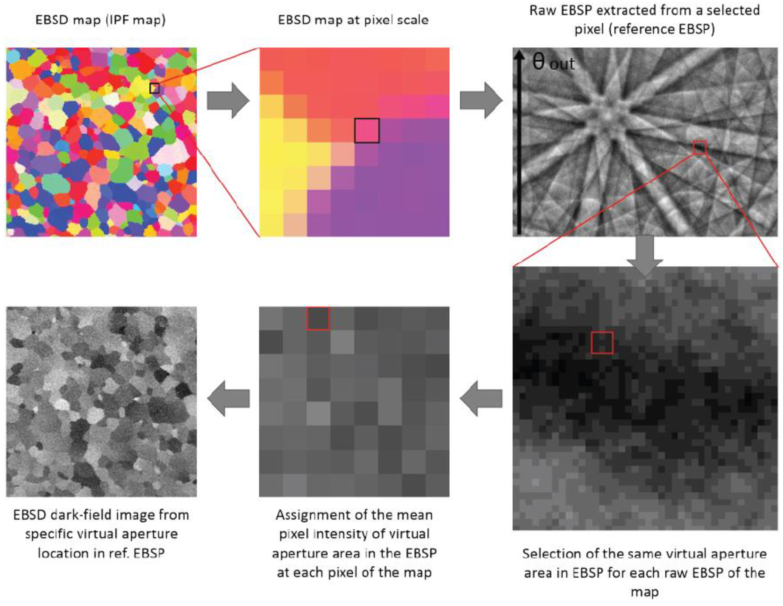
2.3. Description of the Method
3. Results
3.1. EBSD-Dark-Field Imaging
3.2. Compositional Imaging
3.3. Magnetic Domain Imaging
3.4. EBSD-Dark-Field Applied to Transmission Electron Forward Scattering Diffraction
4. Discussion
5. Conclusions
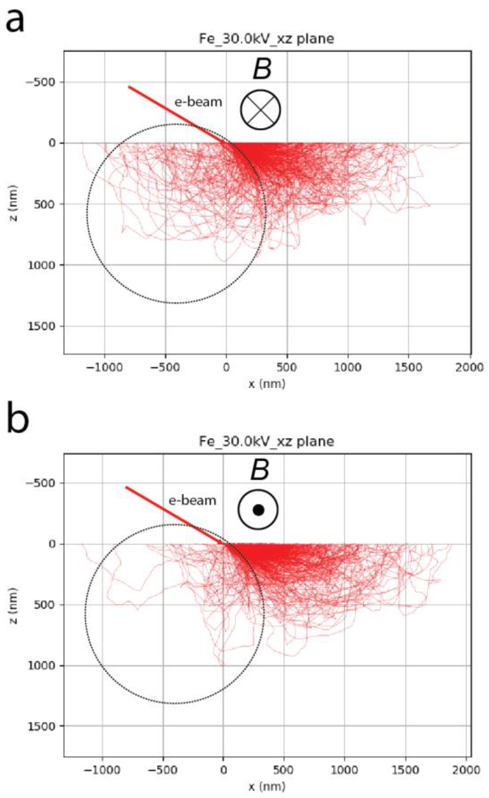
- In conventional mode, i.e., with highly tilted bulk specimens, our results confirm the previously reported findings regarding the contrast obtained versus the polar collection angle of the camera. High emission angles (θout) with respect to the specimen surface are prone to bring compositional contrast into the reconstructed image, while small emission angles carry the topographic contrast component. However, compositional contrast inversion was found when very small collection angles were collected.
- Magnetic domain contrast imaging at elevated tilt angles was optimized by comparing images obtained at different polar emission angles. The highest contrast was obtained with the BSEs emitted at the lowest angles with respect to the specimen surface. Further investigations need to be carried out to confirm, and maybe improve, the contrast if possible.
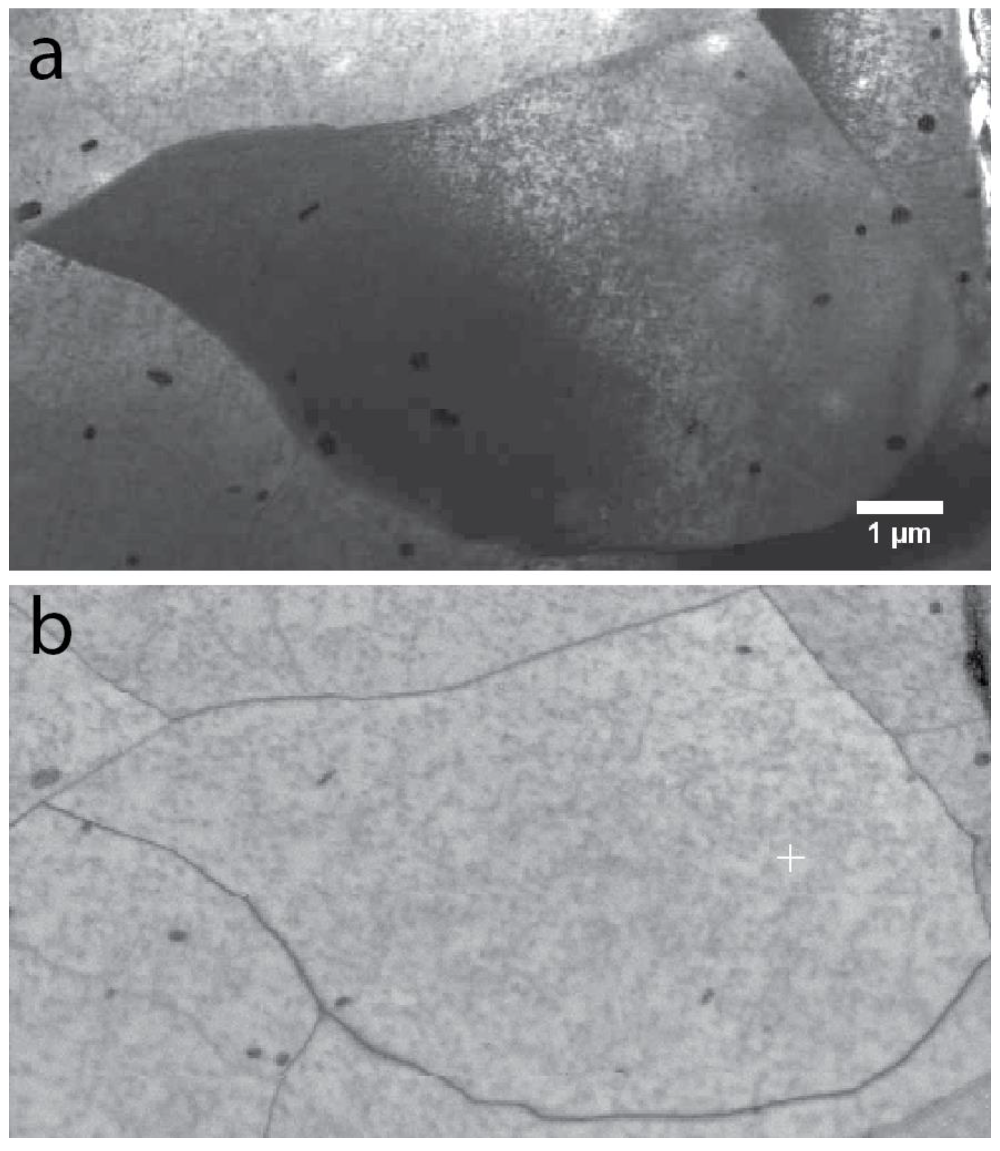
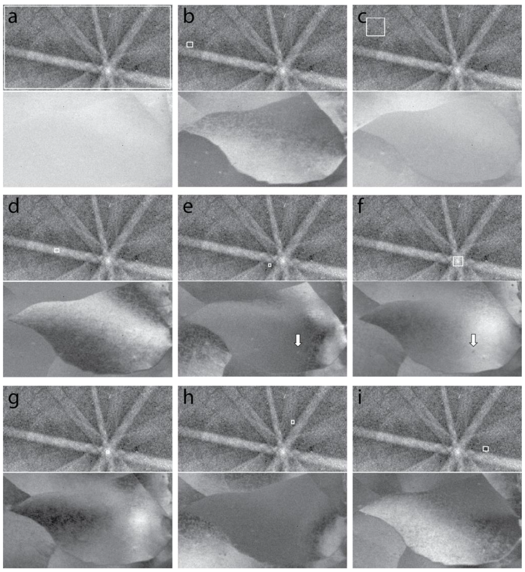
- When the reference image captured by the EBSD camera arises from a crystalline material, the reconstructed images carry the diffraction information related to the specific reflection excited via the virtual beam represented by the pixel array chosen in the reference EBSP. The resulting images thus mimics electron channeling contrast, and allows us to visualize deformation in materials in a new way thanks to the many multiple images that can be generated with this technique from a single scan.
- The diffraction contrast was applied to the transmission mode (t-EBSD) and was capable of generating real transmission dark-field images where the contrast relates to the reflection selected in the reference pattern. The impact on the visibility of fine precipitates inside the matrix was demonstrated, and again, the importance of selecting many different reflections from a single scan was shown to be efficient in characterizing the fine microstructure of a material.
Author Contributions
Funding
Conflicts of Interest
References
- Bell:, D.C.; Erdman, N. Low Voltage Electron Microscopy: Principles and Applications; John Wiley & Sons: Hoboken, NJ, USA, 2012. [Google Scholar]
- Brodusch, N.; Demers, H.; Gauvin, R. Field Emission Scanning Electron Microscopy: New Perspectives for Materials Characterization; Springer: Singapore, 2017; p. 137. [Google Scholar]
- Coates, D.G. Kikuchi-like reflection patterns obtained with the scanning electron microscope. Philos. Mag. 1967, 16, 1179–1184. [Google Scholar] [CrossRef]
- Venables, J.A.; Harland, C.J. Electron back-scattering patterns—A new technique for obtaining crystallographic information in the scanning electron microscope. Philos. Mag. 1973, 27, 1193–1200. [Google Scholar] [CrossRef]
- Schwarzer, R.A.; Field, D.P.; Adams, B.L.; Kumar, M.; Schwartz, A.J. Present state of electron backscatter diffraction and prospective developments. In Electron Backscatter Diffraction in Materials Science; Schwartz, A.J., Kumar, M., Adams, B.L., Field, D.P., Eds.; Springer: Berlin, Germany, 2009; pp. 1–20. [Google Scholar]
- Schwartz, A.J.; Kumar, M.; Adams, B.L.; Field, D.P. Electron Backscatter Diffraction in Materials Science; Springer: Berlin, Germany, 2009. [Google Scholar]
- Zaefferer, S. On the formation mechanisms, spatial resolution and intensity of backscatter kikuchi patterns. Ultramicroscopy 2007, 107, 254–266. [Google Scholar] [CrossRef] [PubMed]
- Steinmetz, D.R.; Zaefferer, S. Towards ultrahigh resolution EBSD by low accelerating voltage. Mater. Sci. Technol. 2010, 26, 640–645. [Google Scholar] [CrossRef]
- Prior, D.J.; Trimby, P.; Weber, U.; Dingley, D.J. Orientation contrast imaging of microstructures in rocks using forescatter detectors in the scanning electron microscope. Miner. Mag. 1996, 60, 859–869. [Google Scholar] [CrossRef]
- Payton, E.J.; Nolze, G. The backscatter electron signal as an additional tool for phase segmentation in electron backscatter diffraction. Microsc. Microanal. 2013, 19, 929–941. [Google Scholar] [CrossRef] [PubMed]
- Wells, O.C.; Gignac, L.M.; Murray, C.E.; Frye, A.; Bruley, J. Use of backscattered electron detector arrays for forming backscattered electron images in the scanning electron microscope. Scanning 2006, 28, 27–31. [Google Scholar] [CrossRef] [PubMed]
- Schwarzer, R.A.; Hjelen, J. Backscattered electron imaging with an EBSD detector. Microsc. Today 2015, 23, 12–17. [Google Scholar] [CrossRef]
- Schwarzer, R.A.; Sukkau, J. Electron back scattered diffraction: Current state, prospects and comparison with X-ray diffraction texture measurement. Banaras Metall. 2013, 18, 1–11. [Google Scholar]
- Nowell, M.M.; Wright, S.I.; Rampton, T.; de Kloe, R. A new microstructural imaging approach through EBSD pattern region of interest analysis. Microsc. Microanal. 2014, 20, 1116–1117. [Google Scholar] [CrossRef]
- Wright, S.I.; Nowell, M.M.; de Kloe, R.; Camus, P.; Rampton, T. Electron imaging with an EBSD detector. Ultramicroscopy 2015, 148, 132–145. [Google Scholar] [CrossRef] [PubMed]
- Brodusch, N.; Demers, H.; Gauvin, R. Dark-field imaging based on post-processing of electron backscatter diffraction patterns in a scanning electron microscope. Microsc. Microanal. 2015, 21, 2031–2032. [Google Scholar] [CrossRef]
- Brodusch, N.; Demers, H.; Gauvin, R. Dark-field imaging based on post-processed electron backscatter diffraction patterns of bulk crystalline materials in a scanning electron microscope. Ultramicroscopy 2015, 148, 123–131. [Google Scholar] [CrossRef] [PubMed]
- Chapman, M.; Callahan, P.; Graef, M. EBSD surface topography determination in a martensitic Au-Cu-Zn alloy. Microsc. Microanal. 2015, 21, 2215–2216. [Google Scholar] [CrossRef]
- Chapman, M.; Callahan, P.G.; De Graef, M. Determination of sample surface topography using electron back-scatter diffraction patterns. Scr. Mater. 2016, 120, 23–26. [Google Scholar] [CrossRef]
- Dorri, M.; Turgeon, S.; Brodusch, N.; Cloutier, M.; Chevallier, P.; Gauvin, R.; Mantovani, D. Characterization of amorphous oxide nano-thick layers on 316l stainless steel by electron channeling contrast imaging and electron backscatter diffraction. Microsc. Microanal. 2016, 22, 997–1006. [Google Scholar] [CrossRef] [PubMed]
- Brodusch, N.; Demers, H.; Gauvin, R. Nanometres-resolution kikuchi patterns from materials science specimens with transmission electron forward scatter diffraction in the scanning electron microscope. J. Microsc. 2013, 250, 1–14. [Google Scholar] [CrossRef] [PubMed]
- Brodusch, N.; Demers, H.; Trudeau, M.; Gauvin, R. Acquisition parameters optimization of a transmission electron forward scatter diffraction system in a cold-field emission scanning electron microscope for nanomaterials characterization. Scanning 2013, 35, 375–386. [Google Scholar] [CrossRef] [PubMed]
- Gauvin, R.; Lifshin, E.; Demers, H.; Horny, P.; Campbell, H. Win X-ray: A new Monte Carlo program that computes X-ray spectra obtained with a scanning electron microscope. Microsc. Microanal. 2006, 12, 49–64. [Google Scholar] [CrossRef] [PubMed]
- Joy, D.C.; Luo, S. An empirical stopping power relationship for low-energy electrons. Scanning 1989, 11, 176–180. [Google Scholar] [CrossRef]
- Heinrich, K.F.; Newbury, D.E.; Yakowitz, H. Use of Monte Carlo Calculations in Electron Probe Microanalysis and Scanning Electron Microscopy: Proceedings of a Workshop Held at the National Bureau of Standards, Gaithersburg, Maryland, October 1–3, 1975; US Dept. of Commerce, National Bureau of Standards: Washington, DC, USA; US Govt. Print. Off.: Washington, DC, USA, 1976.
- Newbury, D.E.; Yakowitz, H.; Myklebust, R.L. Monte carlo calculations of magnetic contrast from cubic materials in the scanning electron microscope. Appl. Phys. Lett. 1973, 23, 488–490. [Google Scholar] [CrossRef]
- Newbury, D.E.; Yakowitz, H.; Myklebust, R.L. A study of type ii magnetic domain contrast in the SEM by Monte Carlo electron trajectory simulation. In Use of Monte Carlo Calculations in Electron Probe Microanalysis and Scanning Electron Microscopy: Proceedings of a Workshop Held at the National Bureau of Standards, Gaithersburg, Maryland, October 1–3, 1975; US Dept. of Commerce, National Bureau of Standards: Washington, DC, USA; US Govt. Print. Off.: Washington, DC, USA, 1976. [Google Scholar]
- Gallaugher, M.; Brodusch, N.; Gauvin, R.; Chromik, R.R. Magnetic domain structure and crystallographic orientation of electrical steels revealed by a forescatter detector and electron backscatter diffraction. Ultramicroscopy 2014, 142, 40–49. [Google Scholar] [CrossRef] [PubMed]
- Reimer, L. Scanning electron microscopy: Physics of image formation and microanalysis. Meas. Sci. Technol. 1998, 11, 1826. [Google Scholar] [CrossRef]
- Wells, O.C. Comparison of different models for the generation of electron backscattering patterns in the scanning electron microscope. Scanning 1999, 21, 368–371. [Google Scholar] [CrossRef]
- Kaboli, S.; Demers, H.; Brodusch, N.; Gauvin, R. Rotation contour contrast reconstruction using electron backscatter diffraction in a scanning electron microscope. J. Appl. Crystallogr. 2015, 48, 776–785. [Google Scholar] [CrossRef]
- Holt, D.B.; Muir, M.D.; Grant, P.R.; Boswarva, I.M. Quantitative Scanning Electron Microscopy; Academic Press: London, UK; New York, NY, USA; San Francisco, CA, USA, 1974. [Google Scholar]
- Aoyama, T.; Nagoshi, M.; Nagano, H.; Sato, K.; Tachibana, S. Selective backscattered electron imaging of material and channeling contrast in microstructures of scale on low carbon steel controlled by accelerating voltage and take-off angle. ISIJ Int. 2011, 51, 1487–1491. [Google Scholar] [CrossRef]
- Aoyama, T.; Nagoshi, M.; Sato, K. Quantitative analysis of angle-selective backscattering electron image of iron oxide and steel. Microscopy 2015, 64, 319–325. [Google Scholar] [CrossRef] [PubMed]
- Banbury, J.R.; Nixon, W.C. The direct observation of domain structure and magnetic fields in the scanning electron microscope. J. Sci. Instrum. 1967, 44, 889. [Google Scholar] [CrossRef]
- Joy, D.C.; Jakubovics, J.P. Direct observation of magnetic domains by scanning electron microscopy. Philos. Mag. 1968, 17, 61–69. [Google Scholar] [CrossRef]
- Fathers, D.J.; Jakubovics, J.P.; Joy, D.C.; Newbury, D.E.; Yakowitz, H. A new method of observing magnetic domains by scanning electron microscopy I. Theory of the image contrast. Phys. Status Solidi A 1973, 20, 535–544. [Google Scholar] [CrossRef]
- Fathers, D.J.; Jakubovics, J.P.; Joy, D.C.; Newbury, D.E.; Yakowitz, H. A new method of observing magnetic domains by scanning electron microscopy. II. Experimental confirmation of the theory of image contrast. Phys. Status Solidi A 1974, 22, 609–619. [Google Scholar] [CrossRef]
- Geiss, R.H.; Keller, R.R.; Read, D.T. Transmission electron diffraction from nanoparticles, nanowires and thin films in an SEM with conventional EBSD equipment. Microsc. Microanal. 2010, 16, 1742–1743. [Google Scholar] [CrossRef]
- Geiss, R.; Keller, R.; Sitzman, S.; Rice, P. New method of transmission electron diffraction to characterize nanomaterials in the sem. Microsc. Microanal. 2011, 17, 386–387. [Google Scholar] [CrossRef]
- Keller, R.; Geiss, R. Transmission ebsd from 10 nm domains in a scanning electron microscope. J. Microsc. 2012, 245, 245–251. [Google Scholar] [CrossRef]
- Suzuki, S. Features of transmission EBSD and its application. JOM 2013, 65, 1254–1263. [Google Scholar] [CrossRef]
- Trimby, P.W. Orientation mapping of nanostructured materials using transmission kikuchi diffraction in the scanning electron microscope. Ultramicroscopy 2012, 120, 16–24. [Google Scholar] [CrossRef] [PubMed]
- Steeds, J.W.; Tatlock, G.J.; Hampson, J. Real space crystallography. Nature 1973, 241, 435. [Google Scholar] [CrossRef]
- Oxford_Instruments. Rapid Characterization of Steel and Ni. Application Note 2017. Available online: http://symmetry.oxford-instruments.com/ (accessed on 1 March 2018).
- Vespucci, S.; Winkelmann, A.; Naresh-Kumar, G.; Mingard, K.P.; Maneuski, D.; Edwards, P.R.; Day, A.P.; O’Shea, V.; Trager-Cowan, C. Digital direct electron imaging of energy-filtered electron backscatter diffraction patterns. Phys. Rev. B 2015, 92, 205301. [Google Scholar] [CrossRef]
- Wilkinson, A.J.; Moldovan, G.; Britton, T.B.; Bewick, A.; Clough, R.; Kirkland, A.I. Direct detection of electron backscatter diffraction patterns. Phys. Rev. Lett. 2013, 111, 065506. [Google Scholar] [CrossRef] [PubMed]
- Reimer, L.; Riepenhausen, M.; Schierjott, M. Signal of backscattered electrons at edges and surface steps in dependence on surface tilt and take-off direction. Scanning 1986, 8, 164–175. [Google Scholar] [CrossRef]
- Yamamoto, T.; Nishizawa, H.; Tsuno, K. Magnetic domain contrast in backscattered electron images obtained with a scanning electron microscope. Philos. Mag. 1976, 34, 311–325. [Google Scholar] [CrossRef]
- Wells, O. Calculation of type ii magnetic contrast in the low-loss image in the scanning electron microscope. In Use of Monte Carlo Calculations in Electron Probe Microanalysis and Scanning Electron Microscopy: Proceedings of a Workshop Held at the National Bureau of Standards, Gaithersburg, Maryland, October 1–3, 1975; US Dept. of Commerce, National Bureau of Standards: Washington, DC, USA; US Govt. Print. Off.: Washington, DC, USA, 1976. [Google Scholar]
- Wells, O.C.; Savoy, R.J. Enhancement of type-2 magnetic contrast in the BSE image in the SEM by a lock-in technique. Scanning 1979, 2, 255–256. [Google Scholar] [CrossRef]
- Ge, Y.; Heczko, O.; Soderberg, O.; Hannula, S.P.; Lindroos, V.K. Investigation of magnetic domains in Ni–Mn–Ga alloys with a scanning electron microscope. Smart Mater. Struct. 2005, 14, S211. [Google Scholar] [CrossRef]
- Ge, Y.; Heczko, O.; Soderberg, O.; Lindroos, V. Various magnetic domain structures in a Ni-Mn-Ga martensite exhibiting magnetic shape memory effect. J. Appl. Phys. 2004, 96, 2159–2163. [Google Scholar] [CrossRef]
- Brodusch, N.; Voisard, F.; Gauvin, R. About the contrast of δ’ precipitates in bulk Al-Cu-Li alloys in reflection mode with a field-emission scanning electron microscope at low accelerating voltage. J. Microsc. 2017, 268, 107–118. [Google Scholar] [CrossRef] [PubMed]


© 2018 by the authors. Licensee MDPI, Basel, Switzerland. This article is an open access article distributed under the terms and conditions of the Creative Commons Attribution (CC BY) license (http://creativecommons.org/licenses/by/4.0/).
Share and Cite
Brodusch, N.; Demers, H.; Gauvin, R. Imaging with a Commercial Electron Backscatter Diffraction (EBSD) Camera in a Scanning Electron Microscope: A Review. J. Imaging 2018, 4, 88. https://doi.org/10.3390/jimaging4070088
Brodusch N, Demers H, Gauvin R. Imaging with a Commercial Electron Backscatter Diffraction (EBSD) Camera in a Scanning Electron Microscope: A Review. Journal of Imaging. 2018; 4(7):88. https://doi.org/10.3390/jimaging4070088
Chicago/Turabian StyleBrodusch, Nicolas, Hendrix Demers, and Raynald Gauvin. 2018. "Imaging with a Commercial Electron Backscatter Diffraction (EBSD) Camera in a Scanning Electron Microscope: A Review" Journal of Imaging 4, no. 7: 88. https://doi.org/10.3390/jimaging4070088
APA StyleBrodusch, N., Demers, H., & Gauvin, R. (2018). Imaging with a Commercial Electron Backscatter Diffraction (EBSD) Camera in a Scanning Electron Microscope: A Review. Journal of Imaging, 4(7), 88. https://doi.org/10.3390/jimaging4070088