Abstract
Materials with nonlinear conductivity are promising for electric field grading in various electrical and electronic devices because of their self-adaptability. In this study, we reported a nonlinear mechanism in fluorinated multi-wall carbon nanotube (F-MWCNT) clusters based on partial discharge in their porous structure. Excellent nonlinear conductivity featuring a low threshold electric field of around 2 kV/mm and a wide range of switching fields was observed after loading an ultra-low F-MWCNT loading ratio of 0.5 wt% into the UV-cured resin. Both experimental and theoretical analyses were performed to explain the underlying nonlinear mechanism. The improved electric field mitigation effect of the composite with F-MWCNT compared with the conventional inorganic fillers like SiC was validated by a flashover test in compressed SF6 gas. Simulations were also conducted to explain the flashover threshold improvement considering the generation of seed electrons for ionization, which was in agreement with the experimental results.
1. Introduction
Localized overstressed electric fields jeopardize the performance of insulation strength in a variety of electronic and electrical devices [1,2,3,4,5,6], potentially leading to partial discharge (PD). A general understanding is that PD undermines the performance of solid insulation and typically serves as a precursor to electrical breakdown [7,8]. Resistive field grading materials (RFGMs) with nonlinear electrical conductivity (σ) offer a viable solution to address the insulation failure caused by an overstressed field [9,10,11,12,13,14,15,16,17,18,19,20]. RFGMs could adapt their σ with the applied electric field, hence alleviating the locally intensified field strengths. Compositing insulation with certain inorganic fillers is the most common way to prepare RFGMs [21,22,23]. The previously reported composites showing field-dependent conductivity properties can be classified in two categories based on the origins of nonlinearities [21]: (1) The nonlinearity derives from the particle–particle contacts. More precisely, the surfaces of the conducting (e.g., pure carbon nanotube) or semi-conducting (e.g., SiC) filler particles are either surrounded by a thin layer of an oxide or another material that could lead to band bending. The changes in the band diagram at the interfaces lead to a nonlinear transport behavior for charge carriers passing from one particle to another. (2) The nonlinearity is an intrinsic property of the filler particles alone. For instance, in ZnO varistor microspheres, double Schottky barriers are formed at each grain boundary. Every single varistor microsphere exhibits a nonlinear σ property. To ensure good nonlinear σ characteristics, the filler content for both categories mentioned above must be greater than the percolation threshold, such that a continuously percolating network can be formed. A large amount of fillers in the matrix deteriorates the processability and the final product performance [24]. Many efforts have been dedicated to reducing the percolation threshold from two main aspects, i.e., using one-dimensional [25] or two-dimensional [26] fillers and controlling filler orientation by self-assembly [14] or external force [27]. However, a low percolation threshold is usually at the expense of processing efficiency due to the additional operational procedures.
As a type of one-dimensional filler, carbon nanotubes (CNTs) have gained extensive attention for their distinctive physical and mechanical properties, which have been considered as ideal inorganic fillers for composite reinforcements [28,29,30]. One route of constructing RFGMs is to load the carbon nanotubes into the insulating matrix [30]. However, a low electrical breakdown threshold restricts their applications in high-voltage engineering. Fluorination is an effective method for modulating CNTs’ crystalline structure, chemical composition, and morphology, which in turn affects the macroscopic electrical conductivity of carbon nanotubes [31,32,33,34,35]. Here, we present a nonlinear conductance mechanism triggered by PD in fluorinated multi-wall carbon nanotube (F-MWCNT) clusters. In contrast to the conventional understanding that PD undermines the performance of insulation materials, we found that a moderate PD process in a limited space could serve as the source of free charge carriers. Excellent nonlinear I–V relationships of the composite with a low switching field threshold can be obtained even if the filler concentration is lower than the percolation threshold. A physical model integrating the double Schottky barriers model for the semiconductor and the dipole model for PD was established to unravel the origin of the nonlinear conductance. Furthermore, RFGMs in the form of surface coatings were prepared, and the flashover characteristics of the prepared SFGMs were tested to validate their effectiveness. Both experimental and simulation results indicate that RFGMs constructed by F-MWCNT clusters can suppress the generation of initial electrons, increasing the threshold voltage for the streamer. We believe that this work provides insights and effective tools for the fabrication of RFGMs with a low electric field threshold and a wide range of switching fields.
2. Results and Discussion
2.1. Specimens Preparation Procedure and Type Description
Initially, F-MWCNTs were prepared by the direct fluorination method. Detailed preparation techniques can be found in the Supplementary Materials Section S1 or in the previous studies [34,35]. To prepare composite materials, F-MWCNTs were doped into the UV-cured resin matrix, as shown in Figure 1. Compared with the conventional thermal curing technique, photo-polymerization is efficient (very fast curing speed), energy-saving (operating at room temperature), and applicable for 3D printing to manufacture complex insulation composites [36,37,38,39]. Note that the morphologies of MWCNTs in the matrix are a crucial factor for their electrical performance. Different topological patterns of MWCNTs were prepared by controlling the ratio of resin to acetone, stirring, heating, and vacuuming time. For instance, to prepare MWCNTs with a porous cluster structure in the composite, a small amount of acetone was used to disperse MWCNTs before co-doping them into the UV-cured resin. During the curing process, the samples were sealed with a quartz cover both above and below. Since the resin cures at a second-level speed, the acetone solution has no time to evaporate. As a result, the MWCNTs remain in the form of a porous clustered state. For comparison, composites loading pristine multi-wall carbon nanotubes (P-MWCNTs) with different states were also prepared by the same processing procedures. Six types of specimens with different dispersion states (uniformly dispersed state, porous cluster state, and compactly aggregated state) were prepared. For convenience, composites containing F-MWCNTs with uniform, porous, and compact dispersion states are denoted as F-MWCNT-u, F-MWCNT-p, and F-MWCNT-c, respectively. By analogy, composites with pristine MWCNTs are also abbreviated as P-MWCNT-p, P-MWCNT-c, and P-MWCNT-u to present different filler dispersion states.
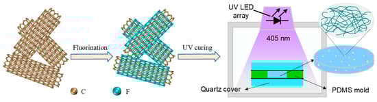
Figure 1.
Schematic illustration of the fabrication procedure of MWCNTs/UV-cured composites.
2.2. Surface and Cross-Sectional Morphologies
Figure 2a reveals the morphology of an F-MWCNT carried out by HRSTEM. The HRSTEM-EDS mappings of element distribution are displayed in Figure 2d (carbon, C) and Figure 2e (fluorine, F). The distribution of the C element is approximately uniform on the vertical side of the nanotube. The presence of the F element confirms the successful grafting of fluorine atoms onto the F-MWNCTs, which has also been verified by the XPS results shown in Figure 2b. Detailed structural characterization of the fluorinated carbon nanotubes used in this study can also be found in the previous research [35,40]. In summary, direct fluorination can lead to a gradual decrease in sp2 carbon content and an increase in C-F bonds, particularly on the outer surface of F-MWCNTs.
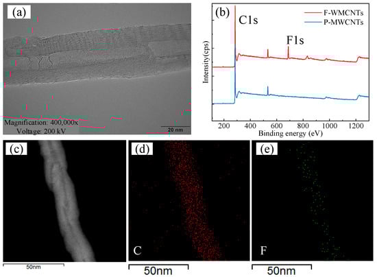
Figure 2.
(a) HRSTEM image of an F-MWCNT. (b) XPS full spectra before and after fluorination. (c) HRSTEM-EDS mapping of an F-MWCNT. Elemental mapping for (d) C element and (e) F element.
F-MWCNT-p forms as porous clusters once the residual acetone volatilizes in the composite. This is validated by the cross-sectional SEM images displayed in Figure 3a,b and by the X-ray microscope (XRM) images displayed in Figure 3c–f. Numerous voids filled with porous FWCNT clusters are generated inside the composite. Both characterization results from SEM and XRM indicate that the size of voids is around 6~10 μm. Based on the XRM 3D reconstruction results, no geometrical connection paths are observed among these voids. Additionally, the overall sphericity of the pores is approximately 0.6 (with 1 representing a perfect sphere).
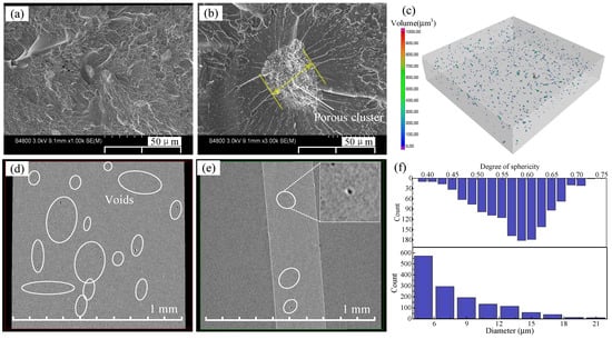
Figure 3.
Cross-sectional SEM images of F-MWCNT-p at a scale of (a) 50 μm and (b) 10 μm. (c) XRM reconstruction results. XRM slices along the (d) horizontal and (e) vertical directions. (f) The statistical results of the sphericity degree and volume of the internal clusters based on XRM characterization.
Figure 4 shows the morphologies of F-MWCNT-c (i.e., composite containing 0.5 wt% F-MWCNT in a compact structure). The SEM results in Figure 4a,b indicate that F-WCNTs in the matrix are aggregated as solid spheres. Characterization from a larger scale by XRM confirms that the aggregated F-MWCNTs have a higher density compared with that of the matrix, as shown in Figure 4d,e. The 3D reconstruction results in Figure 4c show that F-MWCNT-c has a similar geometric distribution compared with F-MWCNT-p. According to the statistical results, the diameter of the aggregates is also below 15 μm, and their sphericity is mostly distributed between 0.55 and 0.65.
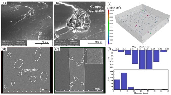
Figure 4.
Cross-sectional SEM images of F-MWCNT-c at a scale of (a) 50 μm and (b) 10 μm. (c) XRM reconstruction results. XRM slices along the (d) horizontal and (e) vertical directions. (f) The statistical results of the sphericity degree and volume of the internal clusters based on XRM characterization.
Apart from F-MWCNT-c and F-MWCNT-p, the cross-sectional morphologies of other composites, including F-MWCNT-u, P-MWCNT-p, P-MWCNT-c, and P-MWCNT-u, are displayed in the Supplementary Materials Section S2. Overall, the morphologies of the fillers in the matrix are in line with expectations, thus providing a foundation for the subsequent comparative studies.
2.3. Frequency-Dependent Dielectric Constant and Field-Dependent Conductivity
For a given insulation system withstanding AC voltage, potential distribution V is governed by:
where absolute permittivity ε = εr·ε0, angular frequency w = 2πf, j is the imaginary part unit, and εr and σ are the relative permittivity and conductivity of the insulation, respectively. In the cases of high frequency or low conductivity (ωε >> σ), the influence of σ could be neglected, and vice versa. In other words, if ωε is comparable to σ, both εr and σ should be considered when dealing with electric field distribution.
Figure 5a gives the frequency-dependent εr of the prepared composites. In general, for composites with pristine MWCNTs, significant increases in εr were observed with decreases in frequency. This prominent increment of εr at low frequency range compared with pure resin indicates the existence of Maxwell–Wagner (M-W) interfacial polarization [41], which takes place in multicomponent dielectrics and refers to the transport of charge carriers at the inter-component interfaces. P-MWCNT-u exhibited a relatively higher εr at 1 MHz and rose to saturation at 20 kHz first. Electrical breakdown occurred at low frequency and contributed to the data deficiency of P-MWCNT-u. Due to the damage of conduction structures, composites with fluorinated MWCNTs show typical relaxation processes of insulating materials. Both F-MWCNT-u and F-MWCNT-c show similar variation tendencies as pure resin. The slight increase in εr could be explained by effective medium theory [42]. A quick increase in εr for F-MWCNT-p occurring at low frequency indicates that the enhancement of interfacial polarization compared with F-MWCNT-c and F-MWCNT-u, as shown in the inset of Figure 5a. This difference should be attributed to the increased conductivity that highlights the contribution of conduction carriers at low frequency [43], which is confirmed by the measurement of I–V characteristics.
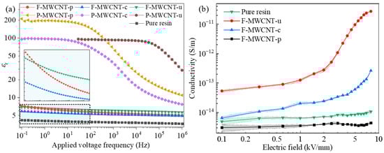
Figure 5.
(a) Frequency-dependent εr and (b) field-dependent σ of prepared UV-cured composites.
Figure 5b shows the calculated σ of the composites versus the electric field in a double-logarithm coordinate. It can be seen that the measurement error is larger at lower voltage levels, while it decreases as the voltage level or conductivity increases. Pure resin exhibits a field-independent σ of 2 × 10⁻¹⁵~4 × 10⁻¹⁵ S/m at 0.1~8 kV/mm. In contrast, all the composites with fluorinated MWCNTs exhibit elevated σ and varying degrees of nonlinearity. Two key parameters (i.e., the nonlinear coefficient α and switching field Eb) are usually adopted to describe the nonlinear behaviors of RFGMs. α could be expressed as 1 + dln(σ)/dln(E) and Eb is the corresponding electric field at the junction point where the field grading regions meet [20]. Larger α and lower Eb are desirable for RFGMs. Notably, F-MWCNT-p exhibits a preferable σ(E) curve for field grading applications with linear grading, nonlinear grading, and pronounced saturated grading stages with the increase in the electric field. A good linear grading effect is observed with α as large as 1.4. When the electric field exceeds 2.0 kV/mm, the composite exhibits nonlinear conduction with α equal to 5.5. Also note that α decreases to 3.5 when the electric field reaches another switching point at 5.4 kV/mm. The physical mechanism of changing α and Eb will be discussed later. As for F-MWCNT–u and F-MWCNT–c, different field-dependent σ profiles were observed even though they have the same filler content. Similar to the case of pure resin, σ of F-WMCNT-u is barely dependent on the electric field and only shifts vertically to the level around 1 × 10⁻¹⁴ S/m. F-WMCNT-c shares the initial value at low electric field with F-MWCNT–u and a similar profile with F-MWCNT–p at the linear grading region. It should be pointed out that for composites with pristine MWCNTs, poor electrical strength causes breakdown even at 0.1 kV/mm; thus, no data were recorded in Figure 5b. Apparently, F-WMCNT-p in this work could realize low Eb and large α with a wide range of switching fields, even though the filler content is as low as 0.5%.
2.4. Flashover Characterization of MWCNT/UV-Cured Composites
In this section, we give a comparative investigation of field grading performance to illustrate the superiority of F-WMCNT-p. Firstly, a UV-cured composite containing 30 wt% commercial SiC particles (SiC-30%) with irregular shapes was also prepared. The SEM images of SiC fillers and the dielectric properties of SiC-30% are shown in the Supplementary Materials Section S4. In terms of nonlinear σ, SiC-30% only yields a linear grading region and a nonlinear grading region. Specifically, α at the linear grading region and nonlinear grading region are 1.1 and 8.5, respectively. The composite remains insulated at low electric field and its nonlinear behavior is pronounced above the switching field of about 3.2 kV/mm. In what follows, a graded structure was designed and coated on epoxy resin wafers, being 100 mm in diameter and 2 mm in thickness. The purpose of deploying RFGMs in a local area is to suppress field enhancements in triple junction regions as well as to reduce Joule heating due to the limited volume of the active region [19]. The sizes of the electrode and the coated local area are described in Figure 6a. The insulation distance between two plate-shaped electrodes (ϕ2 = 20 mm) is 10 mm. The thickness and diameter of the coating are 0.3 mm and 24 mm, respectively. We further conducted finite element analysis based on the commercial software (COMSOL Multiphysics 6.2) to simulate electric field distributions in the frequency domain at 50 Hz. All the geometrical sizes and material properties (εr and σ) in the simulation model were consistent with the actual situations. As illustrated in Figure 6b, the maximum electric field (Emax) of the original insulation structure without local coating material could reach 26.1 kV/mm. In the cases of graded structures deploying SiC-30% and F-MWCNT-p, Emax decreases to 5.7 kV/mm (Figure 6c) and 5.9 kV/mm (Figure 6e), respectively. Due to its high conductivity and permittivity, the position of Emax of the specimen coated with P-MWCNT-p shifts to the point at the coating layer’s edge.
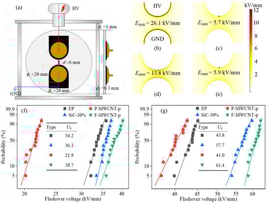
Figure 6.
(a) Layout of insulation structures for measuring flashover voltages in SF6 gas. (b), (c), (d), and (e), respectively, electric distribution of EP, specimens coated with SiC-30%, P-MWCNT-p, and F-MWCNT-p. Weibull distribution of flashover voltages in SF6 gas of (f) 0.1 MPa, and (g) 0.2 MPa.
Flashover tests in an SF6 background were performed to experimentally verify the field mitigation performance of the prepared nonlinear composites. A schematic of the adopted flashover testing system is shown in Figure S4. Weibull plots of AC flashover voltages for the four types of insulation structures described in Figure 6b–e at 0.1 MPa and 0.2 MPa are presented in Figure 6f,g, respectively. In particular, the voltages (U0) at a flashover probability of 63.2%, as a key indicator of surface electrical strength [19], are summarized in the inset table of Figure 6f,g. In general, enhanced surface electrical strength could be achieved with an increase in gas pressure. By applying RFGMs (F-MWCNT-g and SiC-30%), the flashover voltages are remarkably improved, which is in agreement with the simulation results, regarding the reduction in Emax. For instance, in the case of 0.1 MPa, U0 increases from the uniform structure (EP) of 34.2 kV to a structure coated with SiC-30% of 36.1 kV and a structure coated with F-MWCNT-g of 38.7 kV. It is also found that the improvement effect of U0 is positively associated with the gas pressure. For example, U0 of the specimen coated with F-MWCNT-g increases by 13.2% compared to a uniform structure at 0.1 MPa, and this number comes to 40.2% at 0.2 MPa. This is because RFGMs contribute to the reduction in both the electric field strengths at the triple junction area and the critical volume for the discharge inception. Thus, it can be conjectured that the specimens coated with F-MWCNT-g and SiC-30% could exhibit a greater electrical strength improvement effect with further increase in gas pressure. With respect to the comparison of composite types, it is apparent that F-MWCNT-g exhibits better field mitigation since its flashover voltage improves by 40.2% at 0.2 MPa compared with SiC-30% of 31.7%. This is further evidence for the confirmation that the prepared nonlinear composite in this work has advantages compared with conventional RFGMs. As for the composite with P-MWCNTs, its poor electrical strength also brings an adverse impact on the flashover voltage of the graded structure: U0 of the specimen coated with P-MWCNT-g decreases compared with the uniform structure. This discrepancy between the measured flashover voltage and the predicted Emax values in the simulation model is the result of the lack of consideration of the electrical breakdown threshold in the simulations. Breakdown of P-MWCNT-p at a low voltage level reduces the insulation distance, resulting in a decrease in U0.
2.5. Physical Model Establishment and Mechanism Explanation
A common knowledge of the nonlinear conduction mechanism for composites is based on percolation theory. When the filler concentration is below the percolation threshold, the composite behaves as an insulator. Once conduction paths develop with the increase in filler concentration, the composite starts to exhibit nonlinear properties. Since filler in F-MWCNT-c is below the percolation threshold in light of the SEM and XRM results, there should be other mechanisms to explain the nonlinearity in the composites with aggregated F-MWCNTs. To explain the nonlinear behaviors in the F-MWCNT-based composites, the source of free charge carriers should be clarified. Though PD in solid insulation is usually considered harmful since it may contribute to treeing and complete breakdown [44], deposited charges in the solid insulation can also be used to manipulate the field gradient via charge controlling. The increase in conduction due to PD was observed by Song et al., though the phenomenon is still deemed harmful for insulation strength [45]. To verify the origins of charge carriers, PD measurements of F-MWCNT-p were performed in an electromagnetic-shielded room at room temperature. Figure 7a–d show the phase-resolved PD patterns during 6000 cycles of applied electric field (Ea) with different amplitudes. Effective value is adopted here. When Ea = 1.5 kV/mm (Figure 7a), PD incepts and the apparent discharge magnitude is around 4 pC. As Ea increases, the PRPD exhibits a “rabbit ear” pattern, which is consistent with the typical void discharges [46]. When Ea increases to 4 kV/mm (Figure 7d), the discharge number remarkably increases, whereas the maximum apparent discharge magnitude is retained at a level of 17 pC. Note that one major difference between the prepared composite and a traditional specimen with a single and large void is the moderate discharge characteristic [46]. It is concluded that this PD process in the matrix results in the increase in the measured conductivity.
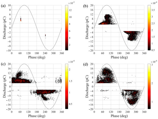
Figure 7.
PRPD patterns of F-MWCNT-p at 50 Hz during 6000 cycles of applied electric field with amplitudes of (a) 1.5 kV/mm, (b) 2 kV/mm, (c) 3 kV/mm, and (d) 4 kV/mm.
Macroscopically, the local field E2 of a dielectric sphere in a uniform electric field E can be calculated by the following equation [47]:
where ε1 and ε2 are the dielectric constants of the matrix and sphere, respectively. As shown in Figure 8a,b, the calculated results agree well with the electrostatic field simulations conducted by COMSOL Multiphysics. Sphere diameter is set as 10 μm to simulate the void in the composite. When ε2 is 80, E2 is significantly lower than 0.68 kV/mm. Hence, a high loading ratio is needed to reduce the gap among fillers for high permittivity fillers like F-MWCNT-c, so as to raise the built-in field inside the sphere and activate the nonlinear conductivity. In the case of εr = 1 (F-MWCNT-p), E2 is stronger than the surroundings. PDs can be triggered at a lower threshold voltage, generating a multitude of free charges inside the bulk. From a microscopic point of view, F-MWCNT-c in Figure 8c is a polycrystalline semiconductor. Double Schottky barriers are formed at the grain boundary. Blatter et al. derived the current density Jdc flowing through a grain boundary [48]. Jdc is given by
where A* is the Richardson constant, T the absolute temperature, e the charge on an electron, V the voltage across the barrier, kB the Boltzmann constant, Φb(V) the barrier height which varies with the applied voltage V, and εξ the energy difference between the bottom of the conduction band and the Fermi level, the total capture probability. At low bias voltage (eV << kBT), the I–V characteristic is Ohmic as Φb barely decreases on this energy scale. With the increase in V, the factor 1 − exp(−eV/kBT) tends toward saturation. This competes with the exponential rise in the current when the barrier Φb decays. The current rises by several orders of magnitude. Finally, at very large V, the current limiting process is given by the finite conductivity of the grains. However, few studies have reported the existence of a saturated stage in composite materials since the current through the electrodes ia has a much more complicated conduction process than Jdc. Electrical breakdown through the conduction path may occur at a high electric field, resulting in a significant increase in ia. Interestingly, three stages of conduction variation described by Equation (3) fit well with our experimental results of F-MWCNT-p displayed in Figure 5b. To explain this similarity, the current through the void is discussed first. As shown in Figure 8d, aggregates form a polycrystalline semiconductor, just like a ZnO microvaristor: double Schottky barriers are formed at the grain boundary, and fluorinated regions create gap states localized between two adjacent grains. The deep traps introduced by F atoms are located at the interface and act as acceptor levels. At the first stage, PDs intercept and generate large quantities of charge carriers. Limited space among FWCNTs restricts the energy of charge carriers, resulting in the moderate discharge process observed in Figure 7a–d. Subsequently, charge carriers generated by PDs are trapped at the surface of FWCNTs, forming a bias voltage between the grain and the boundary. The grain boundary becomes electrically active as a result of charge trapping. In this way, conduction current ia1 through a void due to the moving charge carriers exhibits a similar profile to Jdc. Further, the relationship between currents flowing through a void ia1 and the measured current between two electrodes is discussed. A dipole model for describing the transient physics after PDs is extended [44] and is shown in Figure 8d. In the dipole model, the electromagnetic transients detectable at the electrodes are caused by a dipole moment established in the void as a consequence of gas discharges. Because of the short transient time, the Poisson field caused by space charges is taken into account, and the Laplace field due to the applied voltage is neglected. Since the establishment of ia1 roots in PDs, the assumption of a dipole model is retained. As shown in Figure 8d, to accomplish the current continuity equation, the sum of conduction current through voids (i.e., ia1, ia2, …, ian, n is the number of voids) must be balanced by the displacement current ib through the bulk, which is equal to the current ic through the capacitance C during transient time te. The current balance gives:
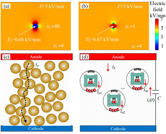
Figure 8.
Field distributions of the composite with (a) a high permittivity filler or (b) a void. Schematic of conduction paths inside the (c) composite with solid polycrystalline fillers like F-MWCNT-c and (d) composite with porous polycrystalline clusters F-MWCNT-p. The direction of the arrow indicates the flow of current.
Because of this correlation, the current through the bulk material also exhibits a typical nonlinear property with a pronounced saturation regime.
To estimate the field mitigation effect, volume–time theory was adopted to describe the relationship between flashover characteristics in compressed SF6 gas and the spatial distribution of the electric field. The flashover probability P(t) for a time-varying voltage can be calculated by Equation (5). Details about the calculation model can be found in our previous research [19].
In Equation (5), Vw is the rate of effective electron avalanche caused by the desorption of negative ions within the critical volume Vcr near the electrode, and Sw is the rate of effective electron avalanche caused by field electron emission at the electrode surface Scr corresponding to the critical volume. α is the electron impact ionization coefficient, η is the electron attachment coefficient, dne1/dt is the expected value of the number of electrons by detachment from SF6- ions per unit time and per unit volume, and dne2/dt is the expected value of the number of electrons by field emission from the cathode surface per unit time and per unit area. The calculation results are displayed in Figure 9. Note that the calculated voltage is the amplitude value. For the same type of material, a higher applied voltage generates more initial electrons from the cathode surface and the critical volume, leading to a faster increase in flashover probability with increasing voltage duration. Elevating the gas pressure can raise the inception voltage for discharge. For instance, in the case of P-MWCNT-p, when the air pressure is 0.1 MPa (Figure 9a), the probability of flashover rapidly increases once the voltage exceeds 51 kV. However, at an air pressure of 0.2 MPa (Figure 9b), the voltage needs to exceed 80 kV for a similar increase in flashover probability. The comparative results of different materials show consistent experimental trends, and as the air pressure increases, the discrepancy between experimental and simulation results becomes smaller.
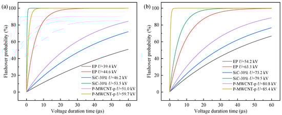
Figure 9.
Flashover probability calculation by volume–time theory. (a) SF6 gas pressure is 0.1 MPa, and (b) SF6 gas pressure is 0.2 MPa.
3. Materials and Methods
3.1. Materials and Specimen Preparation
Multi-walled carbon nanotubes (MWCNTs, 10–20 nm outer diameter, 10–30 μm length) were purchased from Chengdu Organic Chemistry Co., Ltd., Chinese Academy of Sciences, Chengdu, China. The mixed gas for direct fluorination was F2/N2 with a F2 concentration of 10 vol%. After completion of the reaction, the residual gas was pumped out and replaced by N2 for at least 3 cycles and the extracted gas was absorbed by Al2O3 porous microspheres. To achieve a high fluorination degree, the same fluorination process was repeated another time. The TEM images of MWCNTs can be found in Supplementary Materials Figure S1. Then, MWCNTs were adopted to construct RFGMs by photo-polymerization. UV-cured resin (High Temp) was purchased from Formlabs Inc. (Somerville, MA, USA), which is sensitive to the 405 nm light radiation and was used as received. To prepare composites with different dispersed states of MWCNTs, acetone was adopted to dissolve MWCNTs and UV-cured resin in some cases. Firstly, a certain number of MWCNTs were dispersed in acetone. This was followed by the addition of UV-cured resin and mechanical stirring, ultrasonic dispersing, and heating. Subsequently, the mixtures were then placed in a vacuum chamber for a few hours to ensure solvent removal. To control the dispersion states of MWCNTs, processing parameters were optimized, and the finally selected values are listed as follows.
a. MWCNTs with good dispersion states (F-MWCNTs-u and P-MWCNTs-u). Firstly, MWCNTs were dispersed in acetone and then mixed with the UV-cured resin. The mass ratio of MWCNTs, acetone, and UV-cured resin was 0.005:1:1. Subsequently, the mixture was placed in the ultrasonic cleaning instrument (Supmile Inc., KQ5200DE, Suzhou, China, 40 kHz, 600 W) with an ambient water temperature of 60 °C. Mechanical stirring and ultrasonic vibrating were conducted simultaneously for 8 h to guarantee good dispersion of MWCNTs. Thereafter, the mixture was placed in a vacuum chamber at 70 °C for 2 h to ensure complete solvent removal. Finally, the mixture was poured into a silicone mold and cured under UV light of 405 nm, 60 mW/cm2.
b. MWCNTs with porous dispersion states (F-MWCNTs-p and P-MWCNTs-p). The mass ratio of MWCNTs, acetone, and UV-cured resin was 0.005:1:1. Ultrasonic cleaning at 60 °C, accompanied by mechanical stirring, lasted for 0.5 h. Due to the short dispersion time, MWCNTs were still present in the form of agglomerations. Thereafter, the mixture was placed in a vacuum chamber at 70 °C for 0.5 h to remove the majority of the solvent. Residual acetone remaining in the resin was dissolved with MWCNTs, contributing to the generation of a porous structure. Thanks to the fast curing speed of photo-polymerization and the setup of quartz covers on two sides of the specimen, residual acetone could not evaporate during processing. As a result, many voids were formed in the cured composite.
c. MWCNTs with compact dispersion states (F-MWCNTs-c and P-MWCNTs-c). The mass ratio of MWCNTs, acetone, and UV-cured resin was 0.005:0:1. Ultrasonic cleaning at 60 °C, accompanied by mechanical stirring, lasted for 0.5 h. Thereafter, the mixture was placed in a vacuum chamber at 70 °C for 2 h to ensure complete solvent removal. Finally, the mixture was poured into a silicone mold and cured under UV light of 405 nm, 60 mW/cm2.
3.2. Characterization
Morphologies and chemical compositions of carbon nanotubes before and after surface fluorination were measured by a high-resolution transmission electron microscope (HRTEM, JEM2100F, JEOL Ltd., Tokyo, Japan). The cross-sectional morphologies of the composites were characterized by scanning electron microscopes (SEM, S4800, Hitachi, Tokyo, Japan or MAIA3, Tescan, Brno, Czech Republic). Further, the non-destructive sub-micron scale 3D imaging of the composites was performed on an X-ray microscope (XRM, Xradia 610 versa, Zeiss, Oberkochen, Germany) to obtain the statistical information. X-ray photoelectron spectra were measured to confirm the presence of fluorinated groups (XPS, ESCALAB Xi+, Thermo Fisher Scientific, Waltham, MA, USA). Leakage currents through the composites under an electric field with different amplitudes were obtained by a pA electrometer (B2985, Keysight, Santa Rosa, CA, USA) connecting with a high voltage amplifier system (PS365/±10 kV, Stanford Research Systems, Sunnyvale, CA, USA). The diameter and thickness of gold electrode sputtering on the surface of the specimen were 10 mm and 50 nm, respectively. Leakage current was recorded after applying DC voltage for three minutes to exclude the polarization current. Dielectric properties of cured composites were characterized using broadband dielectric spectroscopy (BDS, Concept 80, Novocontrol, Montabaur, Germany). Frequency-dependent (10−1 to 106 Hz) relative permittivity (εr) and dielectric loss (tanδ) at room temperature were recorded. To test for flashover strength, specimens coated with UV-cured composites were placed in a sealed chamber filled with SF6 gas. AC voltages with a frequency of 50 Hz were applied to the insulation, and then the flashover voltages were recorded by a digital oscilloscope (DPO5204B, Tektronix, Beaverton, OR, USA). The PD signals were measured by a PD detector (DDX9121B, HAEFELY AG, Basel, Switzerland) in an electromagnetic-shielded room at room temperature. A low background noise level was maintained to guarantee the accurate capture of weak PD signals. Detailed layouts of the experimental platforms and specific operating steps for flashover and PD measurement can be found in the Supplementary Materials Section S3.
4. Conclusions
In conclusion, we found a peculiar nonlinear conductance mechanism in composite materials. In contrast to the general understanding that PDs undermine the electrical strengths of insulators, we report here an innovative application of PDs that improves the surface electrical strength. Charge carriers were generated by PDs in the voids constructed by aggregated F-MWCNTs. Transport of these carriers inside the voids formed a field-dependent current through the composite. Good nonlinear properties featuring a low threshold electric field of around 2 kV/mm and a wide range of switching fields were observed, though the filler loading ratio was lower than the percolation threshold. The flashover voltage of the insulator coated with F-MWCNT-p in SF6 gas of 0.2 MPa exhibited a 40.2% increase relative to the uncoated specimen. Theoretical analyses were performed to expatiate the underlying physical mechanisms of the observed nonlinear properties, involving the PD of voids and double Schottky barriers generated by F-MWCNT clusters and initial seed electron suppression by electric field mitigation. Our study provides a new approach for surface flashover mitigation of solid insulation.
Supplementary Materials
The following supporting information can be downloaded at: https://www.mdpi.com/article/10.3390/inorganics14010018/s1.
Author Contributions
Conceptualization, W.Z. and C.W.; Methodology, W.Z., Z.L. and L.C.; Investigation, W.Z., Y.W. and L.C.; Data Curation, Y.W. and L.F.; Formal Analysis, W.Z. and Z.L.; Software, L.C. and Y.W.; Validation, Z.L. and L.F.; Resources, C.W.; Visualization, W.Z. and Y.W.; Writing—Original Draft Preparation, W.Z.; Writing—Review and Editing, Z.L., L.C. and C.W.; Supervision, C.W.; Project Administration, C.W.; Funding Acquisition, C.W. All authors have read and agreed to the published version of the manuscript.
Funding
This research was funded by the Smart Grid-National Science and Technology Major Project, grant number 2024ZD0803400, and by the National Natural Science Foundation of China, grant number 52407156.
Institutional Review Board Statement
Not applicable.
Informed Consent Statement
Not applicable.
Data Availability Statement
The data that support the findings of this study are available from the corresponding author upon reasonable request.
Acknowledgments
We appreciate the kind help from Yang Liu from Sichuan University for the preparation of fluorinated carbon nanotubes.
Conflicts of Interest
Authors Wei Zeng, Zhen Li, Yu Wang, Lei Cao and Lei Fu were employed by the company Guizhou Power Grid Co., Ltd. The remaining authors declare that the research was conducted in the absence of any commercial or financial relationships that could be construed as a potential conflict of interest.
Abbreviations
The following abbreviations are used in this manuscript:
| F-MWCNT | Fluorinated Multi-Wall Carbon Nanotube |
| PD | Partial Discharge |
| RFGM | Resistive Field Grading Material |
| P-MWCNT | Pristine Multi-Wall Carbon Nanotube |
| HRTEM | High Resolution Transmission Electron Microscope |
| SEM | Scanning Electron Microscope |
| XRM | X-Ray Microscope |
| BDS | Broadband Dielectric Spectroscopy |
References
- Mesgarpour Tousi, M.; Ghassemi, M. Effects of Frequency and Temperature on Electric Field Mitigation Method via Protruding Substrate Combined with Applying Nonlinear FDC Layer in Wide Bandgap Power Modules. Energies 2020, 13, 2022. [Google Scholar] [CrossRef]
- Li, W.; Li, X.; Guo, B.; Wang, C.; Liu, Z.; Zhang, G. Topology optimization of truncated cone insulator with graded permittivity using variable density method. IEEE Trans. Dielectr. Electr. Insul. 2019, 26, 1–9. [Google Scholar] [CrossRef]
- Zhang, G.; Su, G.; Song, B.; Mu, H. Pulsed flashover across a solid dielectric in vacuum. IEEE Trans. Dielectr. Electr. Insul. 2018, 25, 2321–2339. [Google Scholar] [CrossRef]
- He, M.; Chen, G.; Lewin, P.L. Field distortion by a single cavity in HVDC XLPE cable under steady state. High Volt. 2016, 1, 107–114. [Google Scholar] [CrossRef]
- Hayakawa, N.; Ishiguro, J.; Kojima, H.; Kato, K.; Okubo, H. Fabrication and simulation of permittivity graded materials for electric field grading of gas insulated power apparatus. IEEE Trans. Dielectr. Electr. Insul. 2016, 23, 547–554. [Google Scholar] [CrossRef]
- Shen, Z.; Wang, X.; Zhang, T.; Jia, Z. In situ electric field driven assembly to construct adaptive graded permittivity BaTiO2/epoxy resin composites for improved insulation performance. Appl. Mater. 2020, 20, 100647. [Google Scholar] [CrossRef]
- Shahsavarian, T.; Zhang, D.; McGinnis, P.; Walker, S.; Zhang, Z.; Cao, Y. Altitude readiness of high-voltage IGBTs subjected to the partial discharge at harsh environmental conditions for hybrid electric aircraft propulsion. IEEE Trans. Power Electron. 2022, 37, 3733–3736. [Google Scholar] [CrossRef]
- Li, C.; Shahsavarian, T.; Baferani, M.A.; Cao, Y. Tailoring insulation surface conductivity for surface partial discharge mitigation. Appl. Phys. Lett. 2021, 119, 032903. [Google Scholar] [CrossRef]
- Egorov, D.; Pyrhönen, J.J. One-dimensional model for the nonlinear resistive electric field control in medium-voltage rotating electrical machines. IEEE Trans. Dielectr. Electr. Insul. 2021, 28, 697–703. [Google Scholar] [CrossRef]
- Florkowski, M.; Kuniewski, M. Partial Discharge-Originated Deterioration of Insulating Material Investigated by Surface-Resistance and Potential Mapping. Energies 2023, 16, 5973. [Google Scholar] [CrossRef]
- Metz, R.; Blanc, C.; Dominguez, S.; Tahir, S.; Leparc, R.; Hassanzadeh, M. Nonlinear field dependent conductivity dielectrics made of graphite nanoplatelets filled composites. Mater. Lett. 2021, 292, 129611. [Google Scholar] [CrossRef]
- Zhao, X.; Yang, X.; Hu, J.; Li, Q.; He, J. Globally reinforced mechanical, electrical, and thermal properties of nonlinear conductivity composites by surface treatment of varistor microspheres. Compos. Sci. Technol. 2019, 175, 151–157. [Google Scholar] [CrossRef]
- Yang, X.; Zhao, X.; Hu, J.; He, J. Grading Electric Field in High Voltage Insulation Using Composite Materials. IEEE Electr. Insul. Mag. 2018, 34, 15–25. [Google Scholar] [CrossRef]
- Xu, H.; Wang, R.; Gou, B.; Zhou, J.; Li, L.; Xie, C. Globally enhanced thermal, mechanical and electrical properties of current-field grading composites with self-assembly semiconducting grains on 3D cellulose aerogel scaffolds. Compos. Sci. Technol. 2022, 218, 109197. [Google Scholar] [CrossRef]
- Tousi, M.M.; Ghassemi, M. The effect of type of voltage (sinusoidal and square waveform) and the frequency on the performance of nonlinear field-dependent conductivity coatings for electric field control in power electronic modules. In Proceedings of the 2019 IEEE Conference on Electrical Insulation and Dielectric Phenomena, Richland, WA, USA, 20–23 October 2019; pp. 552–555. [Google Scholar] [CrossRef]
- Christen, T.; Donzel, L.; Greuter, F. Nonlinear resistive electric field grading part 1: Theory and simulation. IEEE Electr. Insul. Mag. 2010, 26, 47–59. [Google Scholar] [CrossRef]
- Li, Z.; Yang, Z.; Xing, Y.; Zhu, W.; Su, J.; Kong, X.; Jiang, J.; Du, B. Improving the electric field distribution in stress cone of hts dc cable terminals by nonlinear conductive epoxy/ZnO composites. IEEE Trans. Appl. Supercond. 2019, 29, 5. [Google Scholar] [CrossRef]
- Zhang, D.; Bi, C.; Gou, B.; Zhou, J.; Zhong, A.; Lin, B.; Cai, H.; Xie, C.; Xu, H.; Wang, R. Field-dependent nonlinear electrical response characteristics in polymer dielectrics with sodium alginate scaffold. Adv. Compos. Hybrid Mater. 2024, 7, 162. [Google Scholar] [CrossRef]
- Wang, C.; Yang, Y.; Hou, C.; Li, W.; Chen, S.; Chen, Z.; Zhang, G. Applicability of surface functionally graded materials for flashover mitigation: From vacuum to compressed SF6 gas. Surf. Coat. Technol. 2025, 508, 132166. [Google Scholar] [CrossRef]
- Can-Ortiz, A.; Laudebat, L.; Valdez-Nava, Z.; Diaham, S. Nonlinear electrical conduction in polymer composites for field grading in high-voltage applications: A review. Polymers 2021, 13, 1370. [Google Scholar] [CrossRef] [PubMed]
- Donzel, L.; Greuter, F.; Christen, T. Nonlinear resistive electric field grading Part 2: Materials and applications. IEEE Electr. Insul. Mag. 2011, 27, 18–29. [Google Scholar] [CrossRef]
- Si, M.; Guo, J.; Hao, J.; Zhao, X.; Randall, C.A.; Wang, H. Cold sintered composites consisting of PEEK and metal oxides with improved electrical properties via the hybrid interfaces. Composites Part B. 2021, 226, 109349. [Google Scholar] [CrossRef]
- Han, Y.; Yang, F.; Zhao, C. Effect of Aged Nonlinear Resistive Field Grading Material on Electric Field Distribution of DC Cone Spacer. Energies 2022, 15, 8361. [Google Scholar] [CrossRef]
- Li, W.; Wang, C.; Jiang, Z.; Chen, L.; Wei, Y.; Zhang, L.; Chen, M.; Yang, X.; Zhang, G. Stereolithography based additive manufacturing of high-k polymer matrix composites facilitated by thermal plasma processed barium titanate microspheres. Mater. Des. 2020, 192, 108733. [Google Scholar] [CrossRef]
- Li, Z.; Du, B.; Yang, Z.; Li, J. Effects of crystal morphology on space charge transportation and dissipation of SiC/silicone rubber composites. IEEE Trans. Dielectr. Electr. Insul. 2017, 24, 2616–2625. [Google Scholar] [CrossRef]
- Zhang, S.; Zhang, H.; Feng, H.; Yan, J.; Liu, P.; Peng, Z. Relaxation processes and conduction mechanism of epoxy resin filled with graphene oxide. IEEE Trans. Dielectr. Electr. Insul. 2017, 24, 519–527. [Google Scholar] [CrossRef]
- Shen, Z.; Xu, C.; Wang, X.; Xin, Z.; Jia, Z. The impact of electric field treatment on nonlinear conductivity of tetra-needle-shaped ZnO whisker/carbon fiber/liquid silicone rubber composites. CSEE J. Power Energy Syst. 2021, 11, 900–908. [Google Scholar] [CrossRef]
- Zhang, K.; Qin, R.; Chen, S.Y.; Liu, X.Y.; Liu, Y. Customizing defect location in MWCNTs/Fe3O4 composites by direct fluorination for enhancing microwave absorption performance. Appl. Surf. Sci. 2023, 612, 155860. [Google Scholar] [CrossRef]
- Gardea, F.; Lagoudas, D.C. Characterization of electrical and thermal properties of carbon nanotube/epoxy composites. Compos. Part B 2014, 56, 611–620. [Google Scholar] [CrossRef]
- Wang, J.; Yu, S.; Luo, S.; Chu, B.; Sun, R.; Wong, C. Investigation of nonlinear I-V behavior of CNTs filled polymer composites. Mater. Sci. Eng. B 2016, 206, 55–60. [Google Scholar] [CrossRef]
- Park, M.S.; Kim, K.H.; Lee, Y.S. Fluorination of single-walled carbon nanotube: The effects of fluorine on structural and electrical properties. J. Ind. Eng. Chem. 2016, 37, 22–26. [Google Scholar] [CrossRef]
- Liu, Y.; Zhang, Y.; Wang, Z.; Lai, W.; Zhang, X.; Wang, X.; Liu, X. Investigation of the dispersion behavior of fluorinated MWCNTs in various solvents. Phys. Chem. Chem. Phys. 2017, 19, 21565–21574. [Google Scholar] [CrossRef]
- Wang, X.; Wu, P. Fluorinated carbon nanotube/nanofibrillated cellulose composite film with enhanced toughness, superior thermal conductivity, and electrical insulation. ACS Appl. Mater. Interfaces 2018, 10, 34311–34321. [Google Scholar] [CrossRef]
- Liu, Y.; Zhang, C.; Huang, B.; Wang, X.; Li, Y.; Wang, Z.; Lai, W.; Zhang, X.; Liu, X. Skin-core structured fluorinated MWCNTs: A nanofiller towards a broadband dielectric material with a high dielectric constant and low dielectric loss. J. Mater. Chem. C 2018, 6, 2370–2378. [Google Scholar] [CrossRef]
- Liu, Y.; Zhang, Y.; Wang, X.; Wang, Z.; Lai, W.; Zhang, X.; Liu, X. Excellent microwave absorbing property of multiwalled carbon nanotubes with skin-core heterostructure formed by outer dominated fluorination. J. Phys. Chem. C 2018, 122, 6357–6367. [Google Scholar] [CrossRef]
- Wang, C.; Yang, Y.; Shi, X.; Li, W.; Sun, G.; Chen, S.; Ran, S.; Zhang, G.; Chen, Z. Secondary electron emission characteristics of 3D-printed ceramic insulators with functionally graded lattice structures. Appl. Phys. Lett. 2025, 126, 121601. [Google Scholar] [CrossRef]
- Wang, C.; Li, W.; Jiang, Z.; Yang, X.; Sun, G.; Zhang, G. UV-cured nanocomposite coating for surface charging mitigation and breakdown strength enhancement: Exploring the combination of surface topographical structure and perfluorooctyl chain. RSC Advances 2020, 10, 16422–16430. [Google Scholar] [CrossRef]
- Wang, C.; Li, W.; Guo, J.; Chen, X.; Jiang, Z.; Li, X.; Guo, B.; Zhang, G. Unraveling the role of surface molecular structure on vacuum flashover for fluorinated copolymers. Appl. Surf. Sci. 2020, 505, 144432. [Google Scholar] [CrossRef]
- Jiang, Z.; Li, W.; Yang, X.; Chen, X.; Wang, C.; Chen, M.; Zhang, G. Low dielectric loss and high breakdown strength photosensitive high-k composites containing perfluoroalkylsilane treated BaTiO3 nanoparticles. Compos. Part B 2020, 192, 108013. [Google Scholar] [CrossRef]
- Chen, S.Y.; Chen, Z.Y.; Ou, Y.L.; Lyu, J.W.; Li, J.N.; Liu, X.Y.; Liu, Y. Flexible multiwalled carbon nanotubes/cellulose nanofibers membrane with rapid temperature increasing induced by interface strengthening. Compos. Part A Appl. S 2024, 177, 107911. [Google Scholar] [CrossRef]
- Yu, Z.; Ang, C. Maxwell-Wagner polarization in ceramic composites BaTiO3-(Ni0.3Zn0.7)Fe2.1O4. J. Appl. Phys. 2002, 91, 794–797. [Google Scholar] [CrossRef]
- Myroshnychenko, V.; Brosseau, C. Finite-element method for calculation of the effective permittivity of random inhomogeneous media. Phys. Rev. E 2005, 71, 016701. [Google Scholar] [CrossRef]
- Runyan, J.; Gerhardt, R.A.; Ruh, R. Electrical properties of boron nitride matrix composites: II, dielectric relaxations in boron nitride-silicon carbide composites. J. Am. Ceram. Soc. 2001, 84, 1497–1503. [Google Scholar] [CrossRef]
- Lemke, E. A critical review of partial-discharge models. IEEE Electr. Insul. Mag. 2012, 28, 11–16. [Google Scholar] [CrossRef]
- Song, B.; Ren, M.; Zhang, Z.; Zhuang, T.; Zhang, C.; Dong, M. Excess conduction induced by partial discharge in polymer. J. Phys. D Appl. Phys. 2020, 53, 485302. [Google Scholar] [CrossRef]
- Li, J.; Si, W.; Yao, X.; Li, Y. Measurement and simulation of partial discharge in oil impregnated pressboard with an electrical aging process. Meas. Sci. Technol. 2009, 20, 105701. [Google Scholar] [CrossRef]
- Kuhn, M.; Kliem, H. Local fields in dielectric nanospheres from a microscopic and macroscopic point of view. IEEE Trans. Dielectr. Electr. Insul. 2009, 16, 596–600. [Google Scholar] [CrossRef]
- Blatter, G.; Greuter, F. Carrier transport through grain-boundaries in semiconductors. Phys. Rev. B 1986, 33, 3952–3966. [Google Scholar] [CrossRef]
Disclaimer/Publisher’s Note: The statements, opinions and data contained in all publications are solely those of the individual author(s) and contributor(s) and not of MDPI and/or the editor(s). MDPI and/or the editor(s) disclaim responsibility for any injury to people or property resulting from any ideas, methods, instructions or products referred to in the content. |
© 2025 by the authors. Licensee MDPI, Basel, Switzerland. This article is an open access article distributed under the terms and conditions of the Creative Commons Attribution (CC BY) license.