Abstract
Light-trapping nanostructures have been widely used for improving solar cells’ performance, but the higher surface recombination and poor electrode contact introduced need to be addressed. In this work, silicon nanostructures were synthesized via silver-catalyzed etching to texturize solar cells. Atomic-layer-deposited Al2O3 passivated the nanotextured cells. A surface recombination velocity of 126 cm/s was obtained, much lower than the 228 cm/s of the SiNX-passivated one. Additionally, the open-circuit voltage (VOC) of the nanotextured cells improved significantly from 582 to 610 mV, as did the short-circuit current (JSC) from 25.5 to 31 mA/cm2. Furthermore, the electrode contact property was enhanced by light-induced plating. A best efficiency of 13.3% for nano-textured cells was obtained, which is higher than the planar cell’s 12%.
1. Introduction
Silicon nanotextured solar cells exhibit ultra-low reflectance and excellent light-trapping properties [1,2,3,4,5,6], which suggests better incident light absorption properties. Optical losses considerably impact solar cell efficiency; therefore, nanotextured solar cells have great potential for performance improvement.
However, until now, the final energy-conversion efficiency of nanotextured c-Si solar cells has not been reasonably satisfactory. Two main shortages impact the performance of such devices. Firstly, the nanotextured silicon surface features many more surface states and defects [7,8]. This increases the surface recombination by an order of magnitude. Secondly, the nanotextured surface fluctuates highly, and the space size is very small. Screen-printed electrodes can only lay on the tips of nanotextures. The small contact area increases the contact resistance [9,10]. Surface recombination impacts the open-circuit voltage and short-circuit current, while the electrode contact property influences the fill factor (FF) of the solar cell.
This work aims to find effective techniques to address these side-effects introduced by nanotextures and improve the efficiency of c-silicon solar cell. Firstly, silicon nano-textures were fabricated using a controllable silver-catalyzed etching. Then, passivation layers of Al2O3 and SiNX were used separately on silicon nanotextured solar cells. The Al2O3 showed a better passivation than SiNX did on the silicon nanotextured cells. Then, the open-circuit voltage (VOC) and FF of three groups of cells were measured, which indicated that the screen-printed electrode contact property of the nanotextured solar cells was poor. Several techniques were used previously to supplementally improve the contact of the screen-printed electrode, such as a heavily doped emitter [10] or selective texturing [11]. These techniques could enhance the contact property, but they introduced more surface recombination or the process was too complex. To address this problem, a light-induced plating (LIP) technique was utilized in this work to enhance the screen-printed electrode contact. The process of LIP brings no extra drawbacks and is a promising electrode-improving supplemental technology for nanotextured solar cells. A best efficiency of 13.3% was obtained for nanotextured cells, which was higher than that of the planar control cell. Due to the passivation and contact enhancement, nanotextures can exhibit a light-trapping advantage and improve the efficiency of solar cells. Following this laboratory experiment, we will try to apply the techniques to large-area black silicon solar cells in the future.
2. Experimental Details
In the experiment, 4 inch p-type (100) CZ Si polished wafers were used as the substrate. The resistance of each c-Si wafer was 1–5 Ω·cm, and the thickness was 280 μm. All wafers were divided into three groups: nanotextured sample A (NS-A), nanotextured sample B (NS-B), and planar. Wafers were well cleaned firstly. The cleaning process contained the following steps: Step 1: cleaning in a mixed solution (H2SO4:H2O2 = 4:1) at 120–150 °C for 15 min; Step 2: cleaning by deionized water at 80 °C for 2 min; Step 3: cleaning in a 2% HF solution at room temperature for 30 s; Step4: cleaning by deionized water at room temperature for 2 min.
After the cleaning process, an Ag thin film with a thickness of 10 nm was deposited on one side of the NS-A and NS-B wafers by electronic beam evaporation. The wafers of these two groups were annealed via rapid thermal treatment at 600 °C for 5 min. After the treatment, Ag nanoparticles were distributed on the front surface of the Si wafers [12]. Then, these samples were etched in an aqueous mixed solution of deionized water, HF (5.0 M), and H2O2 (0.5 M) at 25 °C for 5 min to form a nanotextured surface. The surface color of the wafers was black after being immersed in a concentrated HNO3 solution for 2 h, which removed the Ag remnants.
Secondly, all three groups of wafers (NS-A, NS-B, and planar) underwent the same conventional diffusion process (liquid POCl3 as a doping source, at 850–900 °C for about 1 h) to form a p–n junction, and the sheet resistivity was 60 Ω/sq. Then, 80 nm SiNX was deposited on the NS-A and planar groups via plasma-enhanced chemical vapor deposition (PECVD), whereas, on the NS-B wafers, 100 nm Al2O3 was grown via atomic layer deposition (ALD). Up until this process, the samples remained whole wafers.
Then, the wafer samples were isolated into cells with an area of 20 × 20 mm2 using mechanical dicing equipment. The edges of wafers were simultaneously removed in this process. Then, the back and front sides of each cell were screen-printed with Al and Ag pastes to form Al-BSF and the front electrode, followed by baking the individual pastes. Finally, dried cells were cofired in a belt furnace to achieve an Ohmic contact at both ends. The current–voltage (I–V) measurements were tested using a Keithley2400 I–V curve tracer and a SANYO solar simulator under standard test conditions (AM 1.5 irradiation, T = 300 K, and P = 1 kW/m2). The lifetime (τeff) for samples in this work was measured by the PV-2000 equipment.
Furthermore, light-induced plating was introduced to enhance the screen-printed electrode contact of the fabricated samples. The principle of LIP is shown in Figure 1a. The solar cell sample was immersed in AgNO3 liquid solution. The light incidence on the surface of the solar cell generated electron–hole pairs. The electrons moved from the back to the surface electrode of the solar cell and reduced the silver ions (Ag+) into Ag atoms. Then, these Ag atoms accumulated on the electrode to form Ag layers. Through this process, spacing and gaps in the electrode could be filled and the contact property could be improved. The back-contact of the solar cell was connected to a silver anode with an external voltage (VE) to neutralize the light-generated holes; otherwise, the holes would oxidize the back-contact metal. Figure 1b shows the LIP experimental platform used in this work.
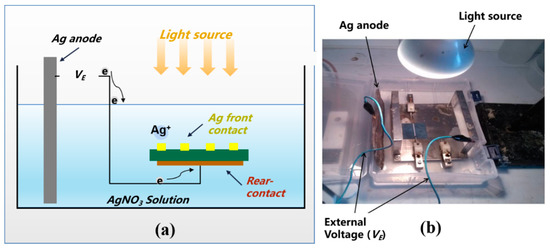
Figure 1.
(a) The schematical principle of light-induced-plating. (b) Photograph of the LIP platform in our lab.
3. Results and Discussion
The plane view and the cross-sectional view of the surface of NS-A were analyzed using field-emission scanning electron microscopy (SEM) in a HITACHI S4800 device, shown in Figure 2a,b. Additionally, Figure 2c,d show the plane view and cross-sectional view of the surface of NS-B. The structure dimensions of the nanotextured surface were about 50–100 nm horizontally and 0.5 μm vertically. These two groups of samples were different in passivation layers. For NS-A, the passivation layer was PECVD-grown SiNX and did not conformally cover the silicon nanotextured surface. Gaps in the silicon nano-textures still existed. Meanwhile, for NS-B, an ALD-grown Al2O3 layer passivated the surface and conformally covered the whole surface of the nanostructures. The top-view image shows that the tips of the silicon nanostructures were roundly coated with Al2O3 film and appeared as semi-spheres. Additionally, the cross-sectional view shows that the gaps in the nanostructures were filled by the grown Al2O3 layer. This well-coated passivation film and silicon nanosurface indicated that the dangling bonds and surface defects could be saturated; thus, an excellent chemical passivation effect was obtained.
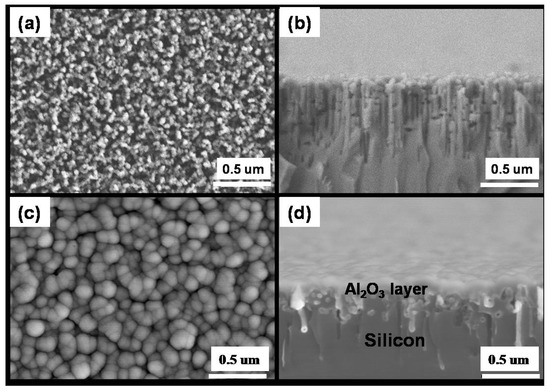
Figure 2.
SEM images of silicon nanostructures with passivation layers of (a,b) 80 nm SiNX and (c,d) 100 nm Al2O3. The Al2O3 layer filled the gaps in the silicon nanostructures through deposition.
3.1. Light-Trapping Property of Nano-Texture
The reflection curves in the 300–1100 nm wavelength range of the three groups of cells are shown in Figure 3, as well as the blank wafer and non-passivated nanotextured wafer as references. It can be seen that the nanotextured wafer with no passivation layer deposited (NS wafer) exhibited very low reflectance—lower than 3% in the 300–1100 nm range. The SiNX-passivated nanotextured cells only showed a slight increase within the 800–1000 nm range and remained low in the other wavebands, while the Al2O3-deposited nanotextured cells showed slight little fluctuations at wavelengths of 600 and 800 nm.
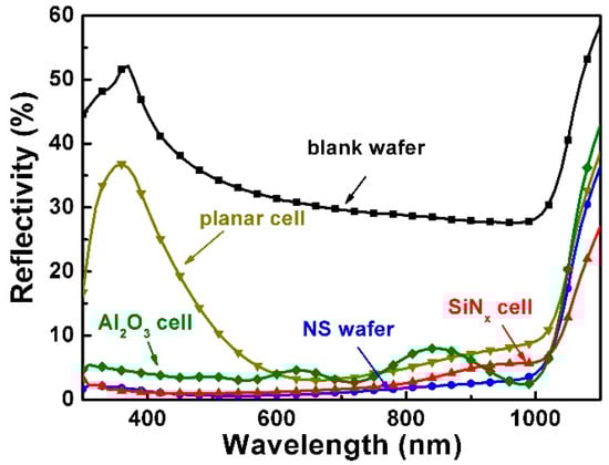
Figure 3.
The reflectance of silicon nanotextured solar cells with passivation layers of 80 nm SiNX and 100 nm Al2O3. For comparison, the reflectance of a blank wafer, as well as that of a planar cell coated with 80 nm SiNX and a silicon nanotextured wafer without deposition, is also plotted.
The weighted average reflectance (Ra) of samples and reference wafers was calculated under AM1.5 standard conditions using Equation (1), and the Ra values are listed in Table 1. Here, λ is the wavelength, R(λ) is the measured reflectance, and N(λ) is the solar flux under AM1.5 standard conditions [13].

Table 1.
The weighted average reflectance (Ra) of samples and reference wafers.
This confirms that nanotextured Si wafers exhibited ultra-low reflectance compared with blank wafers. Furthermore, this result suggests that the passivation films (SiNX and Al2O3) deposited on the nanotextured surface did not significantly impact the ultra-low reflectance, even though the thicker Al2O3 layer densely covered the nanotextured surface and wrapped the nanowire, according to the SEM images in Figure 2. Compared with planar cells, the nanotextured cells had much lower reflectance in the short wavelength range. Here, the SiNX layer of the planar cell effectively lowered the surface reflectance in the long wavelength range.
3.2. Surface Passivation of Nanotexture
To characterize the surface recombination of the samples, the effective lifetimes (τeff) were measured in terms of quasi-steady-state photo-conductance (QSS-PC) at 1 sun injection level, using PV-2000 equipment, as shown in Figure 4. The mapping results of NS-A were nonuniform across the whole area, which indicates that the SiNX layer did not removed passivate the whole nano-textured surface effectively. The measured τeff of NS-A was 43.5 μs on average, much lower than the values of 97.4 μs for NS-B and 143.3 μs for planar cells. For NS-B and planar cells, the mapping results were uniform across the whole surface. The effective lifetime was determined by the recombination both on the surface and in the bulk of the silicon solar cell, which can be calculated by Equation (2).
where τbulk is the lifetime of bulk silicon substrate, S is the surface recombination velocity of the cell, and W is the thickness of the solar cell. In this work, all the samples were based on the same silicon wafers; therefore, the τbulk value for all groups of cells could be considered the same. As a result, the difference in τeff values among different groups here was mainly determined by the surface recombination. The passivation effects of different layers could be evaluated by τeff measurements. Given a τbulk value of silicon wafer of 1 ms and a wafer thickness of 280 μm, the surface recombination velocity for the three groups of cells could be calculated as 228, 126, and 86 cm/s, respectively. This clearly shows that the Al2O3 layer led to more effective passivation on the silicon nanotextured surface than the SiNX layer did. Additionally, the nanotextured surface had more recombination than the planar surface did.
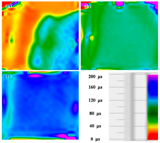
Figure 4.
Minority carrier lifetime (at 1 sun injection level) images of (a) silicon nanotextured wafer coated with 80 nm SiNX, (b) silicon nanotextured wafer coated with 100 nm Al2O3, and (c) silicon blank wafer coated with 80 nm SiNX.
The injection level-dependent lifetimes of the three groups of solar cells were measured, as shown in Figure 5a. It can be seen that the silicon nanotextured samples coated with SiNX showed an overall lower lifetime. When compared with the planar cell, the lifetime of NS-A was lower within the whole injection range, which suggests that the nanotexturing process introduced significant defects and traps and considerably increased the surface recombination of the silicon samples. For the NS-A and NS-B samples, the Al2O3 layer showed a better passivation effect than the SiNx layer did on the nanotextured surface.
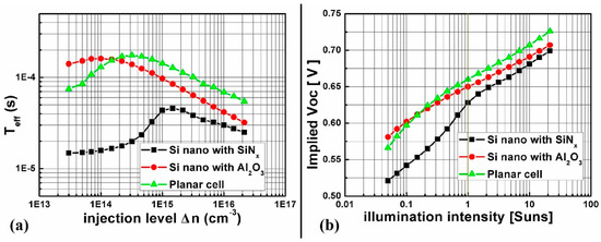
Figure 5.
(a) Injection level dependent lifetime τeff; (b) illumination intensity implied-VOC of the three groups of experimental samples.
The τeff values varied with injection density level (∆n) according to measurement, and this can be attribute to multiple mechanisms of bulk and surface recombination. There are three fundamental bulk-recombination mechanisms: radiative recombination, Auger recombination, and recombination through defects in the bandgap (Shockley–Read–Hall recombination) [14,15,16]. Shockley–Read–Hall (SRH) recombination is an indirect process, calculated using the Shockley–Read–Hall model [14]. Furthermore, there are two main surface-recombination mechanisms: interface-state recombination and space-charge-region (SCR) recombination [17,18].
At a low injection density level (∆n), SRH and SCR recombination are the dominant mechanisms. SRH recombination is less injection-density-dependent, and SCR recombination decreases as ∆n increases. Thus, at a high ∆n, radiative, Auger, and interface-state recombination become the predominant mechanisms. These three kinds of recombination increase as ∆n increases. As a result, the measured τeff values in Figure 5a initially increased and then declined as ∆n increased.
Quasi-steady-state photo-conductance (QSS-PC) measures the average excess carrier concentration. Assuming that the carrier concentration is constant through the base, the effective minority carrier lifetime is commonly used for characterization. An alternative interpretation of the minority carrier lifetime is to determine the open-circuit voltage (VOC) of the device. This parameter is called implied-VOC [19] and is determined from the carrier concentrations:
where kT/q is the thermal voltage, NA is the doping concentration, ∆n is the excess carrier concentration, and ni is the intrinsic carrier concentration. The illumination intensity dependent implied-VOC values of the three groups samples are plotted in Figure 5b. The implied-VOC improved as the illumination intensity increased since the excess carrier concentration considerably determines the parameter. The implied-VOC at 1 sun illumination intensity for NS-A, NS-B, and the planar cell was 628, 650, and 660 mV, respectively.
3.3. Electrode Contact Enhancement Via Light-Induced Plating (LIP)
The current–voltage (I–V) measurements for the samples were tested using a Keithley2400 I–V curve tracer and a SANYO solar simulator under standard test conditions (AM 1.5 irradiation, T = 300 K, and P = 1 kW/m2). According to the I–V parameters in Figure 6a and Table 2, the nanotextured solar cells passivated via Al2O3 exhibited a better performance than those passivated via SiNX. The average open-circuit voltage (VOC) was improved from 582 to 610 (mV), the short-circuit current density (JSC) improved from 25.5 to 30.8 mA/cm2, and the efficiency improved from 8.6% to 10%. The main factor determining the VOC of a cell is its surface recombination. Lower surface recombination increases the collection probability of the carriers, thus increasing the JSC. Compared with the planar cell, NS-B exhibited higher JSC values, which could mainly be attributed to the excellent light-trapping property of the nanotexture. However, the efficiency of the NS-B cell was still lower than that of the planar cell, and the lower fill factor of the nanotextured solar cells contributed a large proportion. As shown in Table 1, the average series resistance of NS-B was 1.13 Ω, which is much larger than the planar cell value of 0.41 Ω. The poor electrode contact of the nanotextured cell impacted its performance [20,21,22].
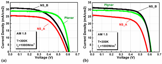
Figure 6.
(a) I–V curves of the sample solar cells under standard test condition (AM 1.5 irradiation, T = 300 K, and P = 1 kW/m2) before light-induced plating. (b) I–V curves of the cells after the light-induced plating. It can be observed that the FF and JSC were improved after the enhancement.
Table 2.
Electrical parameters for the silicon nanostructure-textured solar cells.
In order to quantify the influence of the electrode contact property on the solar cell performance, the suns VOC values of the three groups of solar cells were measured and are shown in Figure 7, normalized to JSC. The suns VOC measurement provided the I–V curve of a solar cell without the effect of series resistance. The suns VOC values of the NS-A, NS-B, and planar cells were 613, 630, and 643 mV, respectively. These values are lower than the implied VOC measured above, but still much higher than the actual VOC value. Moreover, the suns- F value was close to 0.8 for the samples, which is significantly higher than the actual FF value of 0.5–0.7. Additionally, the gap between the suns FF and actual FF values was larger for NS cells than for planar cells. These results suggest that the electrode of the nanotextured solar cells was poorly contacted and needs enhancement.
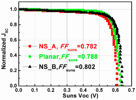
Figure 7.
The VOC and FF of the three groups of cells under the condition of ideal electrode contact (RS = 0). The figure is normalized to JSC. The suns VOC values here are 613, 630, and 643 mV, respectively.
To enhance the electrode contact of the nanotextured solar cells, light-induced plating (LIP) was introduced [23,24] for all three groups of solar cells. This technique can fill the voids along the electrode–silicon interface and reduce the contact resistance. Schematic images and SEM photographs of the interface before and after LIP are shown in Figure 8.
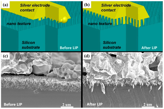
Figure 8.
Schematic images of interface between electrode and nanotextured silicon substrate (a) before LIP and (b) after LIP. SEM photographs of the interface (c) before and (d) after LIP.
Figure 6b and Table 3 show the electrical parameters of the cells after the LIP enhancement. The series resistance (RS) was considerably reduced from 1.13 to 0.33 for NS-B cells, the FF improved from 0.53 to 0.7, and the efficiency improved from 10% to 13.3%. For planar cells, the performance also improved, but only slightly, since the electrode contact of planar cells was better than that of nanotextured cells initially.
Table 3.
Electrical parameters for the silicon nanostructure-textured solar cells after LIP.
After the LIP enhancement, the efficiency of NS-B cells was higher than that of planar cells (12%). The higher JSC of NS-B cells contributed most to the improved efficiency. Additionally, the excellent light trapping of the nanotextures increased the JSC of the solar cells. Compared to other electrode-enhancing techniques, LIP has advantages. Firstly, it brings no extra side-effects. Secondly, the process is simple and can be implemented in scale production. Additionally, the effect of LIP is significant, especially in nanotextured solar cells.
According to Figure 9, the quantum efficiency (after LIP) of NS-B cells was higher than that of NS-A and planar cells. Notably, the NS-B cells’ quantum efficiency was lower than that of planar cells within wavelengths shorter than 400 nm, as the surface recombination of NS-B cells was still higher than that of planar cells. Under this condition, the addition of nanotextures on the silicon solar cells led to an improvement in JSC of 2.5 mA/cm2 and in efficiency by 1.3%, indicating excellent optical advantages.
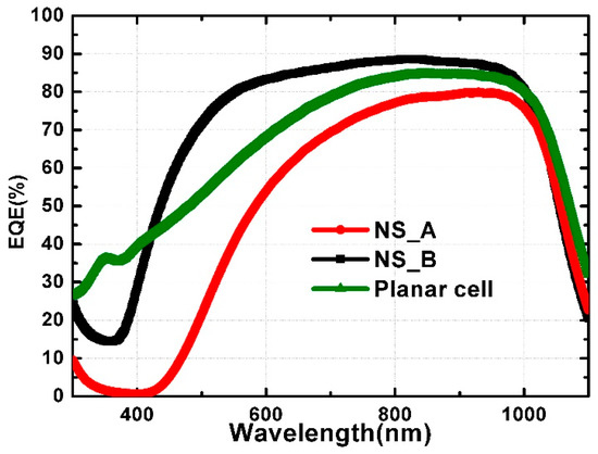
Figure 9.
The quantum efficiency of three groups of cells after LIP. NS-B cells showed the best performance.
Additionally, it should be pointed out that planar solar cells with Al2O3 passivation were not included as a control group in this work. To give a better comparison, the reflectance (Figure A1) and I–V parameters (Figure A2 and Table A1) of SiNX- and Al2O3-passivated planar cells fabricated in our previous experiment are included in Appendix A. It can be seen that Al2O3-passivated planar solar cells showed similar performance to SiNX-passivated ones.
4. Conclusions
In this work, techniques for improving the efficiency of silicon nanotextured solar cells were investigated. A passivation layer of Al2O3 was used instead of SiNX on the silicon nanotextured solar cells. Al2O3 showed a better passivation than SiNX did on nanotextured cells. The JSC of nanotextured cells was better than that of the planar cells due to the light-trapping ability of nanotextures. To enhance the screen-printed electrode contact property of nanotextured solar cells, the LIP technique was introduced. Compared with other previously used electrode-improving supplemental techniques, LIP brings no extra drawbacks and is promising for scale production. After the light-induced-plating, a best efficiency of 13.3% was obtained for nanotextured cells, which was higher than that of the planar control cell. The quantum efficiency confirmed that the light absorption enhancement improved the cells’ performance.
Author Contributions
Conceptualization, R.J.; formal analysis, B.D.; funding acquisition, R.J.; methodology, B.D. and Z.X.; project administration, Z.J. and X.L.; supervision, R.J.; writing—original draft, B.D.; writing—review and editing, R.J., X.Y. and D.X. All authors have read and agreed to the published version of the manuscript.
Funding
This work was funded by the National Natural Science Foundation of China (NSFC, Grant Nos. 51602340, 51702355).
Data Availability Statement
Not applicable.
Acknowledgments
This work was conducted at the Institute of Microelectronics, Chinese Academy of Sciences.
Conflicts of Interest
The authors declare no conflict of interest.
Appendix A
The performance of planar p-type c-Si solar cells fabricated in our previous experiments were included as a supplementary comparison.

Figure A1.
The reflectance of silicon planar solar cells with passivation layers of 80 nm SiNX and 100 nm Al2O3.

Figure A2.
The I–V curves of the planar solar cells under standard test conditions (AM 1.5 irradiation, T = 300 K, and P = 1 kW/m2).
Table A1.
The electrical parameters of previously fabricated planar solar cells with Al2O3 (100 nm) and SiNX (80 nm) passivation.
Table A1.
The electrical parameters of previously fabricated planar solar cells with Al2O3 (100 nm) and SiNX (80 nm) passivation.
| Group | VOC (mV) | JSC (mA/cm2) | FF (%) | Eff (%) | RS (Ω·cm2) |
|---|---|---|---|---|---|
| Al2O3-coated planar (4 cells) | 614 ± 7 | 29.7 ± 1.1 | 62.6 ± 5.6 | 11.4 ± 0.3 | 0.56 ± 0.27 |
| SiNX-coated planar (4 cells) | 607 ± 3 | 29.0 ± 0.4 | 63.3 ± 3.4 | 11.1 ± 0.5 | 0.59 ± 0.16 |
References
- Es, F.; Baytemir, G.; Kulakci, M.; Turan, R. Metal-assisted nano-textured solar cells with SiO2/Si3N4 passivation. Sol. Energy Mater. Sol. Cells 2017, 160, 269–274. [Google Scholar] [CrossRef]
- Nirmal, A.; Kyaw, A.K.K.; Wang, J.; Dev, K.; Sun, X.; Demir, H.V. Light trapping in inverted organic photovoltaics with nanoimprinted ZnO photonic crystals. IEEE J. Photovolt. 2017, 7, 545–549. [Google Scholar] [CrossRef]
- Sun, T.; Xu, Z.; Xu, H.; Zhao, W.; Peng, J. Direct Tailoring the Si Substrate for Antireflection via Random Nanohole Nanoimprint. J. Nanosci. Nanotechnol. 2015, 15, 1297–1303. [Google Scholar] [CrossRef] [PubMed]
- Su, G.; Jia, R.; Dai, X.; Tao, K.; Sun, H.; Jin, Z.; Liu, X. The Influence of Black Silicon Morphology Modification by Acid Etching to the Properties of Diamond Wire Sawn Multicrystalline Silicon Solar Cells. IEEE J. Photovolt. 2018, 8, 937–942. [Google Scholar] [CrossRef]
- Lei, W.; Zhang, H.; Qin, F.; Bai, X.; Ji, Z.; Dan, H. Performance enhancement of pc-Si solar cells through combination of anti-reflection and light-trapping: Functions of AAO nano-grating. Opt. Commun. 2017, 385, 205–212. [Google Scholar]
- Jiang, Y.; Shen, H.; Pu, T.; Zheng, C.; Tang, Q.; Gao, K.; Wu, J.; Rui, C.; Li, Y.; Liu, Y. High efficiency multi-crystalline silicon solar cell with inverted pyramid nanostructure. Sol. Energy 2017, 142, 91–96. [Google Scholar] [CrossRef]
- Tsakalakos, L.; Balch, J.; Fronheiser, J.; Korevaar, B.A.; Sulima, O.; Rand, J. Silicon nanowire solar cells. Appl. Phys. Lett. 2007, 91, 233117. [Google Scholar] [CrossRef]
- Hamilton, B. Porous Silicon. Semicond. Sci. Technol. 1995, 10, 1187–1207. [Google Scholar] [CrossRef]
- Schmidt, V.; Wittemann, J.; Senz, S.; Gösele, U. Silicon nanowires: A review on aspects of their growth and their electrical properties. Adv. Mater. 2009, 21, 2681–2702. [Google Scholar] [CrossRef]
- Chen, C.; Jia, R.; Li, H.; Meng, Y.; Liu, X.; Ye, T.; Kasai, S.; Tamotsu, H.; Wu, N.; Wang, S.; et al. Electrode-contact enhancement in silicon nanowire-array-textured solar cells. Appl. Phys. Lett. 2011, 98, 143108. [Google Scholar] [CrossRef]
- Dou, B.; Jia, R.; Sun, Y.; Li, H.; Chen, C.; Jin, Z.; Liu, X.; Xu, X. Enhanced electrode-contact property of silicon nano-textured solar cells via selective etching. Sol. Energy 2014, 99, 95–99. [Google Scholar] [CrossRef]
- Dou, B.; Jia, R.; Li, H.; Chen, C.; Meng, Y.; Ding, W.; Liu, X.; Ye, T.; Wang, Y. Maskless fabrication of selectively sized silicon nanostructures for solar cell application. J. Vac. Sci. Technol. B 2012, 30, 041401. [Google Scholar] [CrossRef]
- Menna, P.; Francia, G.D.; Ferrara, V.L. Porous silicon in solar cells: A review and a description of its application as an AR coating. Sol. Energy Mater. Sol. Cells 1995, 37, 13–24. [Google Scholar] [CrossRef]
- Richter, A.; Glunz, S.W.; Werner, F.; Schmidt, J.; Cuevas, A. Improved quantitative description of Auger recombination in crystalline silicon. Phys. Rev. B 2012, 86, 165202. [Google Scholar] [CrossRef]
- Luo, D.; Su, R.; Zhang, W.; Gong, Q.; Zhu, R. Minimizing non-radiative recombination losses in perovskite solar cells. Nat. Rev. Mater. 2020, 5, 44–60. [Google Scholar] [CrossRef]
- Tyagi, M.S.; van Overstraeten, R. Minority carrier recombination in heavily-doped silicon. Solid-State Electron. 1983, 26, 577–597. [Google Scholar] [CrossRef]
- Bonilla, R.S.; Hoex, B.; Hamer, P.; Wilshaw, P.R. Dielectric surface passivation for silicon solar cells: A review. Phys. Status Solidi A 2017, 214, 1700293. [Google Scholar] [CrossRef]
- Schmidt, J.; Werner, F.; Veith, B.; Zielke, D.; Steingrube, S.; Altermatt, P.P.; Gatz, S.; Dullweber, T.; Brendel, R. Advances in the Surface Passivation of Silicon Solar Cells. Energy Procedia 2012, 15, 30–39. [Google Scholar] [CrossRef]
- Xu, G.; Hallam, B.; Hameiri, Z.; Chan, C.; Yao, Y.; Chong, C.; Wenham, S. Over 700 mV Implied Voc on p-Type CZ Silicon Solar Cells with Double-Sided Laser Doping. Energy Procedia 2013, 33, 33–40. [Google Scholar] [CrossRef][Green Version]
- Feng, Z.; Jia, R.; Dou, B.; Li, H.; Jin, Z.; Liu, X.; Li, F.; Zhang, W.; Wu, C. Enhanced properties of silicon nano-textured solar cells enabled by controlled ZnO nanorods coating. Sol. Energy 2015, 115, 770–776. [Google Scholar] [CrossRef]
- Liang, X.; Shu, L.; Lin, H.; Fang, M.; Zhang, H.; Dong, G.; Yip, S.; Xiu, F.; Ho, J.C. Inverted Silicon Nanopencil Array Solar Cells with Enhanced Contact Structures. Sci. Rep. 2016, 6, 34139. [Google Scholar] [CrossRef]
- Disney, C.E.R.; Pillai, S.; Green, M.A. The Impact of parasitic loss on solar cells with plasmonic nano-textured rear reflectors. Sci. Rep. 2017, 7, 12826. [Google Scholar] [CrossRef] [PubMed]
- Dou, B.; Jia, R.; Li, H.; Chen, C.; Ding, W.; Meng, Y.; Xing, Z.; Liu, X.; Ye, T. High performance radial p-n junction solar cell based on silicon nanopillar array with enhanced decoupling mechanism. Appl. Phys. Lett. 2012, 101, 183901. [Google Scholar] [CrossRef]
- Lennon, A.; Yao, Y.; Wenham, S. Evolution of metal plating for silicon solar cell metallisation. Prog. Photovolt. Res. Appl. 2013, 21, 1454–1468. [Google Scholar] [CrossRef]
Publisher’s Note: MDPI stays neutral with regard to jurisdictional claims in published maps and institutional affiliations. |
© 2021 by the authors. Licensee MDPI, Basel, Switzerland. This article is an open access article distributed under the terms and conditions of the Creative Commons Attribution (CC BY) license (https://creativecommons.org/licenses/by/4.0/).