
Communication

Laser-Induced Thermal Annealing of CH3NH3PbI3 Perovskite Microwires
1
School of Optoelectronic Engineering and Instrumentation Science, Dalian University of Technology, Dalian 116024, China
2
School of Microelectronics, Dalian University of Technology, Dalian 116024, China
3
Department of Photonics, National Cheng Kung University, Tainan 70101, Taiwan
*
Authors to whom correspondence should be addressed.
Photonics 2021, 8(2), 30; https://doi.org/10.3390/photonics8020030

Submission received: 7 January 2021 / Revised: 23 January 2021 / Accepted: 24 January 2021 / Published: 26 January 2021
(This article belongs to the Special Issue Optoelectronic Materials and Their Applications)

Abstract

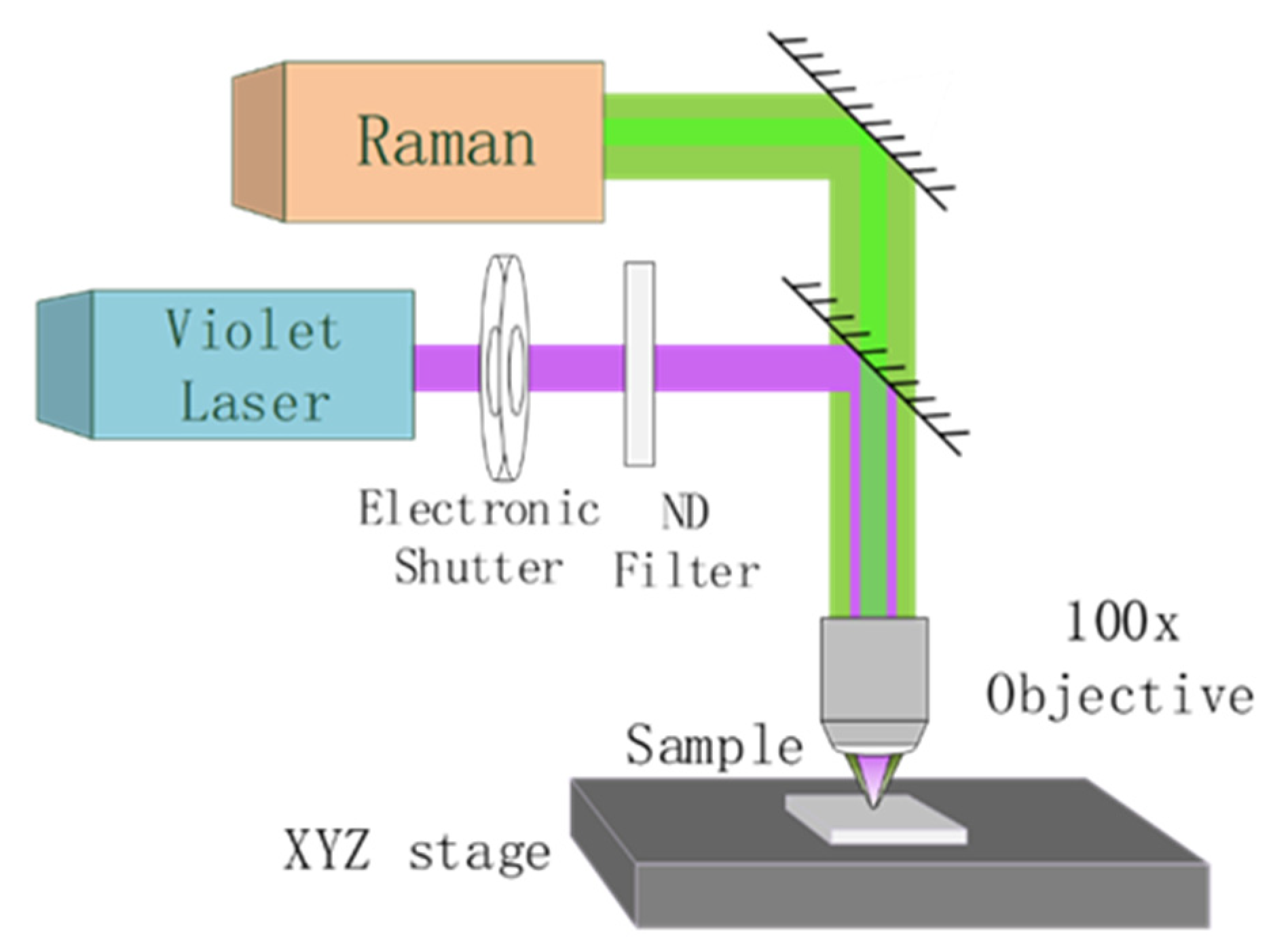
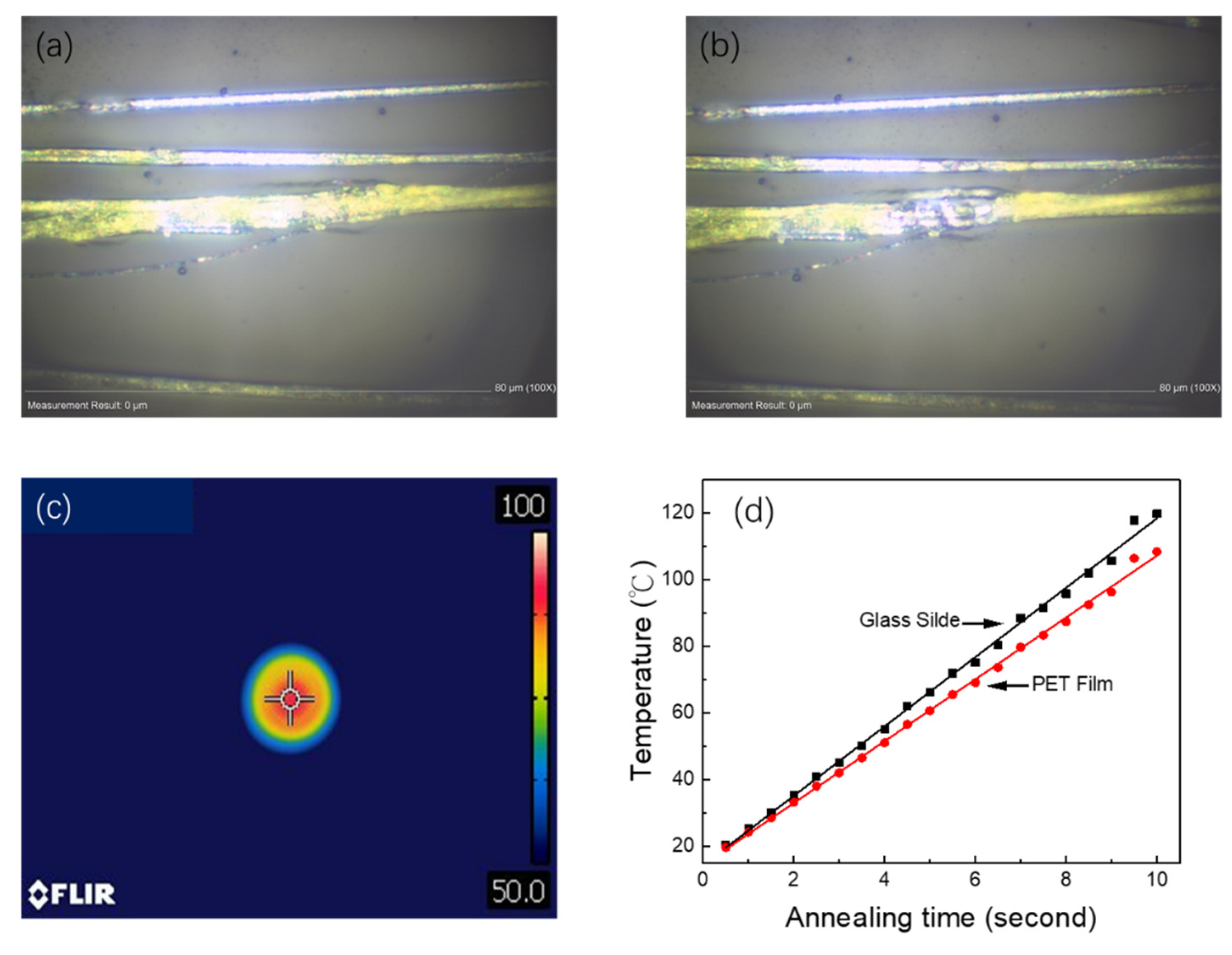
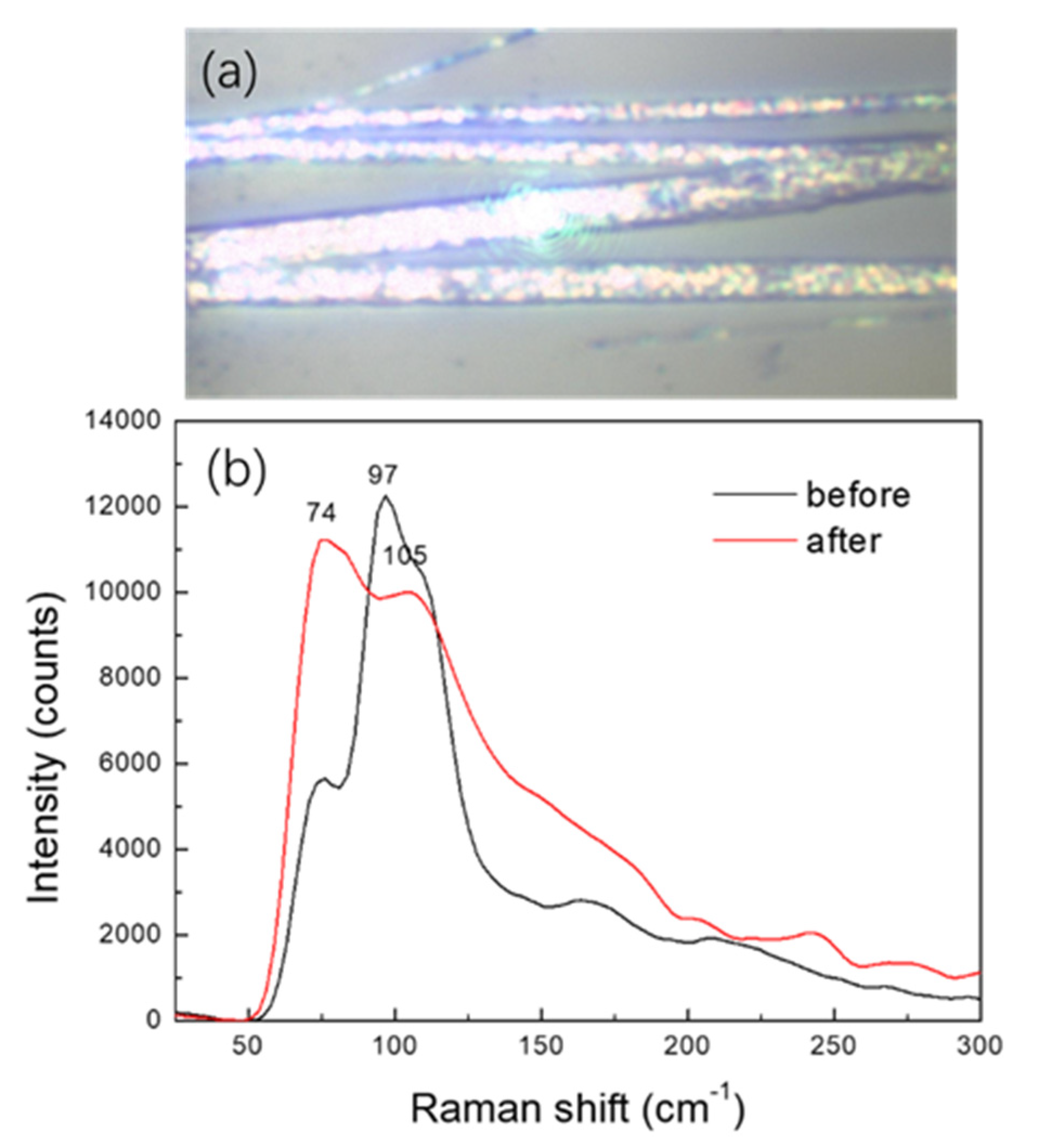
Perovskite microwires have a larger surface-to-volume ratio and better photoelectric conversion efficiency than perovskite films. The degree of crystallization also affects the optoelectrical performances of perovskite microwires. Laser annealing was regarded as a tool for crystallization. High light absorption induced fast heating process. A 405 nm violet laser located near the absorption peak of typical perovskite films was employed as the annealing laser. In an in situ experimental design, the annealing laser beam was combined into the micro Raman measurement system. Real-time information of the annealing and crystallization was provided. Many excellent works were done, and typically needed offline optoelectronic measurements. An mW-level continuous-wave laser beam can provide enough kinetic energy for crystalline in perovskite microwires. The thermal distribution of the perovskite microwire under the annealing laser beams was considered here. Polarized Raman signals can provide evidence of the perovskite microwires crystallization. This work offered the novel approach of an on-site, real-time laser-induced thermal annealing design for perovskite microwires. This approach can be used in other material procedures. Intensity-dependent conditions were crucial for the annealing processes and analyzed in detail. The substrate effect was found. This proposed scheme provided integrated novel, scalable, and highly effective designs of perovskite-based devices.
Keywords: perovskite; laser annealing; crystallization; Raman perovskite; laser annealing; crystallization; Raman