Abstract
We report the synthesis and characterization of pure ZnO, pure CeO2, and ZnO:CeO2 mixed oxide thin films dip-coated on glass substrates using a sol-gel technique. The structural properties of as-prepared thin film are investigated using the XRD technique. In particular, pure ZnO thin film is found to exhibit a hexagonal structure, while pure CeO2 thin film is found to exhibit a fluorite cubic structure. The diffraction patterns also show the formation of mixed oxide materials containing well-dispersed phases of semi-crystalline nature from both constituent oxides. Furthermore, optical properties of thin films are investigated by performing UV–Vis spectrophotometer measurements. In the visible region, transmittance of all investigated thin films attains values as high as 85%. Moreover, refractive index of pure ZnO film was found to exhibit values ranging between 1.57 and 1.85 while for CeO2 thin film, it exhibits values ranging between 1.73 and 2.25 as the wavelength of incident light decreases from 700 nm to 400 nm. Remarkably, refractive index of ZnO:CeO2 mixed oxide-thin films are tuned by controlling the concentration of CeO2 properly. Mixed oxide-thin films of controllable refractive indices constitute an important class of smart functional materials. We have also investigated the optoelectronic and dispersion properties of ZnO:CeO2 mixed oxide-thin films by employing well-established classical models. The melodramatic boost of optical and optoelectronic properties of ZnO:CeO2 mixed oxide thin films establish a strong ground to modify these properties in a skillful manner enabling their use as key potential candidates for the fabrication of scaled optoelectronic devices and thin film transistors.
1. Introduction
Zinc oxide (ZnO) is an essential and promising material for several modern technological applications owing to its high transmittance of visible light, wide direct band gap of 3.37 eV, extremely large exciting binding energy, high electrochemical stability, high semiconductor resistivity and non-toxicity [1,2,3,4]. In recent years, the interest in ZnO thin films has been significantly increased with the realization of devices such as optoelectronics [5,6], LED [7], UV-laser [8], solar cells [9,10], sensors [11] and other optical coating applications [12]. Moreover, ceria (CeO2) thin film has attracted much attention and widely explored due to its extraordinary characteristics. Mainly, its high transmittance of visible light, wide direct band gap of 3.2 eV, high stability, high dielectric constant and high refractive index [13,14,15], consequently, ceria thin films have been used for technological applications such as optoelectronics [16,17], solid oxide fuel cells [18,19], energy storage [20,21] and catalysts [22,23,24,25]. Moreover, CeO2 has been used as a corrosion protective coating [26,27].
Non vacuum depositing techniques such as pin coating, dip coating and spray pyrolysis coating are commonly used for the deposition and synthesis of thin films. Owing to their appealing features such as low cost, easiness and simplicity, such methods are considered as important research tools for the preparation of as-grown metal mixed thin films. In particular, spin coating is one of the most important research techniques due to its high reproducibility over a widespread viscosity range. However, this method suffers from a serious drawback as it is not appropriate for large scale industrial production. On the other hand, dip coating is a widely-used method for easy and fast deposition of thin films on substrates of large areas. It is appropriate for depositing materials on both side of large-area substrate. If the deposition rate and power conversion efficiency are high, spray coating can be easily performed for relatively uniform and high-quality coatings.
Previous works have reported that co-deposition of mixed metal oxides such as ZnO:CeO2 could yield mixtures of exceptional properties such as high UV absorption, controllable optical band gap, good photoluminescence, high extinction coefficient, anticorrosive properties and high refractive index [28]. In recent years, ZnO:CeO2 mixed oxides thin films have been used for essential applications, such as sensors [29,30], catalysts [31,32], fuel cells applications [33], antibacterial applications [34], corrosion protective coating [35], and UV filters [36].
The motivation to explore, measure and interpret the optical and optoelectronic properties of ZnO:CeO2 mixed oxide thin films stems from their anticipated optical applications. They have been widely used as key potential components for UV filters and high refractive index optical devices. Sun-proofs and sun-protectors products are used largely especially in regions that are exposed to sunshine for most of the year. They serve as efficient filters for energetic UV-light. As a result, they have been implemented increasingly nowadays to produce materials for human skin protection from the hazardous UV radiations. Owing to their serious drawbacks such as fractional degradation and, consequently high UV absorption, when exposed to UV light, organic UV blockers are not appropriate especially for people with medical records that indicate potential photo allergy [36]. Furthermore, mixed metal oxide thin films are reported as good candidates for the fabrication of single-mode polymer waveguides. The superiority of such guides over other types of waveguides is that a slight adjustment of the refractive index may accomplish the total reflectance and therefore effective wave guiding. However, single-mode polymer waveguides suffer from serious drawback caused by Fresnel losses result from the mismatch in the refractive index values between the metal oxides and the semiconductor-based device. This can be tackled and resolved by choosing metal oxides with high refractive indices [37]. For that reason, thin films exhibit high refractive indices have enticed substantial consideration for advanced optoelectronic devices such as light emitting diode devices [38], photoresists for 193-nm immersion lithography [39], high performance substrates for advanced display devices [40] and micro lens components for charge coupled devices or complementary metal oxide semiconductor [41]. As mentioned before, it is important to investigate the optoelectronic properties of ZnO: CeO2 mixed oxides thin films. In this study, we report the crystallography, microstructure, crystal defects and optoelectronic properties of ZnO:CeO2 mixed oxides thin films fabricated by sol–gel method.
2. Experimental Details
2.1. Preparation Pure ZnO and Pure CeO2 Solution
The pure ZnO/pure CeO2 solution was prepared by dissolving 4.38 g of zinc acetate dehydrated (Zn (CH3CO2)2 2H2O) and 2.21 g of Ce (III) nitrate hexahydrate (Ce(NO3)3·6H2O) separately in 50 mL 2-methoxyethanol. ZnO solution was then mixed thoroughly on a magnetic stirrer for 50 min at room temperature, while CeO2 solution was then mixed thoroughly on a magnetic stirrer for 60 min at 65 °C. Then, the ethanolamine of 1.7 mL and acetylacetone of 1.5 mL as a stabilizer was added to the ZnO and CeO2 solutions, respectively, in terms of drop by drop while stirring the solutions until they become transparent. The resulting mixtures was stirred for 40 min to get homogeneous solutions. The solutions were filtered by paper-filter with 0.45 μm in dimension [1,2,42].
2.2. Preparation of ZnO:CeO2 Mixed Oxides Solution
ZnO:CeO2 mixed oxides solution was prepared by mixing pure ZnO solution with pure CeO2 solution with three different concentration ratios (ZnO:CeO2, 0.75:0.25, 0.50:0.50, 0.25:0.75) using magnetic stirrer for 1 h at room temperature.
2.3. Deposition of ZnO:CeO2 Mixed Oxides Thin Films
To prepare the desired mixed-oxides thin films, pure ZnO, pure CeO2 and mixed ZnO:CeO2 are deposited for 2 h on pre-cleaned glass substrates by dip coating technique. The deposited thin films are then air dried at 110 °C in an oven at atmospheric pressure for 15 min in order to evaporate the solvents and organic residues. In the final step of the synthesis, we anneal the deposited dried pure ZnO, pure CeO2 and ZnO:CeO2 mixed oxides thin films in air at 500 °C for 2 h. The procedure followed ensures that the obtained thin films are structurally optimized [1,2].
2.4. Characterizations of ZnO:CeO2 Mixed Oxides Thin Films
Crystallinity of ZnO:CeO2 mixed oxides thin films is investigated by Powder XRD (Malvern Panalytical Ltd., Malvern, UK) (220–230 VAC 50/60 Hz 40 A) using Cu Kα1 ray with a wavelength of 0.1540598 nm at room temperature from angles of incident photon on the surface ranges from 10° to 70° with a step of 0.02° with an energy resolution of 20%. Angular resolution: 0.026° FWHM on LaB6, and Angular reproducibility < 0.0002°. Maximum angular speed of 15 deg./s. The optical transmittance and reflectance spectra are measured using UV–Vis spectrophotometer (U-3900H) with the total internal integrating sphere at room temperature.
3. Result and Discussion
3.1. X-Ray Diffraction (XRD) Analysis
Figure 1 shows the XRD patterns of pure ZnO, pure CeO2 and ZnO:CeO2 mixed oxide thin films annealed at 500 °C for 2 h. Pure ZnO thin films exhibit peaks at Bragg’s angles of 32.13°, 34.75° and 36.58° corresponding to (100), (002) and (101) crystallographic planes, respectively. In addition, XRD patterns confirm that ZnO thin film is polycrystalline and exhibits wurtzite hexagonal structure [3,43]. In addition, the main peaks of pure CeO2 thin film are observed at Bragg’s angles of 28.89°, 33.54° and 47.88° corresponding to CeO2 crystallographic planes indexed by Miller indices of (111), (200) and (220), respectively. Comparison of observed and standard ‘’ () planes as matched with JCPDS cards no. 034–394 indicates that CeO2 thin film is polycrystalline and exhibit cubic phase with fluorite structure [44]. Furthermore, XRD patterns indicate that pure CeO2 and ZnO thin films have a higher degree of crystallinity than that of ZnO:CeO2 mixed thin films. Careful examination of XRD patterns reveal that ZnO:CeO2 mixed thin films encompass distinct crystalline phases of ZnO and CeO2 components [45]. XRD patterns of ZnO:CeO2 mixed thin films containing 25%–75% of CeO2 NPs reveal that the intensity of ZnO reflections at (100), (002) and (101) decrease quite rapidly while that of the CeO2 (111) peak increases. This could be understood in terms of the amount of scattered X-ray from Ce4+ and Zn2+ ions. The diffraction factor f of Ce4+ ions is higher than that of Zn2+ ions. Since f of an atom depends mainly on where is the scattering angle and is the wavelength of X-ray and atomic number Z, it is challenging to identify lighter atoms in presence of heavier atoms. The diffraction pattern of ZnO is much weaker than that of CeO2 [44]. Obviously, the individual peak positions of CeO2 and ZnO remain unchanged in the XRD pattern of ZnO:CeO2 composite oxides. This provides substantial evidence that XRD pattern of ZnO:CeO2 consists mainly of distinct phases of ceria and ZnO. The existence of weaker peaks indicates that dissolving of small amount of ZnO in ceria and vice versa is possible for a certain extent. Mixing ZnO hexagonal lattice with CeO2 fluorite leads to a drastic change of diffraction pattern. Thus, lattice constant of the composite changes significantly. The lattice constant ‘’ for the cubic phase structure and ‘’ for the hexagonal phase structure are evaluated as:
where is the inter-planar spacing and can be determined using Bragg’s law (). The lattice constants of pure ZnO and CeO2 thin films are presented in Table 1. The lattice constants ( and ) of pure wurtzite ZnO thin film are calculated to be 3.216 Å and 5.161 Å, respectively, in a good agreement with those reported in [46]. The lattice constant of pure CeO2 thin film is found to be 5.350 Å is in a good agreement with that reported in [44].
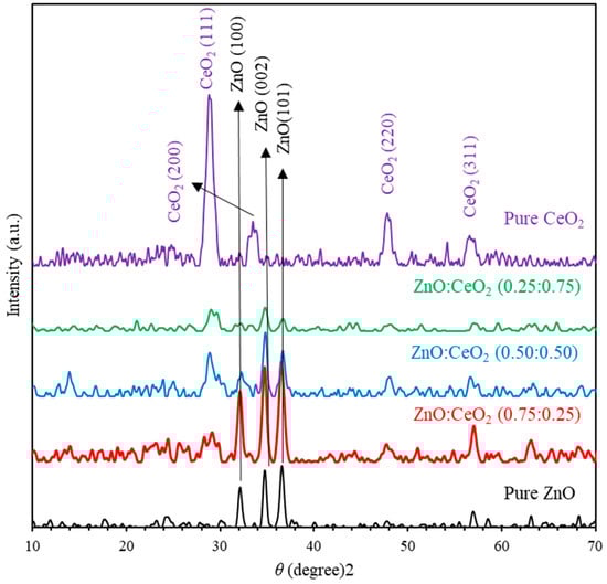
Figure 1.
The X-ray diffraction (XRD) patterns of pure ZnO, pure CeO2 and ZnO:CeO2 mixed oxides thin films.

Table 1.
The structure and Lattice constants (a and c) for pure ZnO and pure CeO2 thin films.
To elucidate the elastic properties of synthesized mixed oxide thin films, crystallite size and microstrain originated from the lattice misfitting and mismatching are deduced from the peak width and the shift of the 2θ peak position [47]. Fundamentally, average can be computed from the Debye Scherrer’s formula, [48,49] where is the wavelength of the X-ray (), (in radians) is the full width at half maximum (FWHM), is Bragg’s angle and = 0.94 is the Scherrer constant [50,51]. The average microstrain [48,52]. The estimated values of and of ZnO:CeO2 mixed oxide thin films are plotted as functions of CeO2 concentrations as shown in Figure 2. The value of D of pure ZnO and CeO2 thin films was found to be 18.93 nm and 9.26 nm, respectively. However, D of ZnO:CeO2 mixed oxide thin films containing 25%, 50% and 75% of CeO2 were found to be 12.09 nm, 11.58 nm and 11.50 nm, respectively. Obviously, Figure 2 shows an inverse relationship between and D which could be attributed to the decrease in the volume occupied by constituents inside the combined crystalline structure. In addition, as the volume of the unit cells increases, the total surface area is increased causing a shift in planes positions [53].
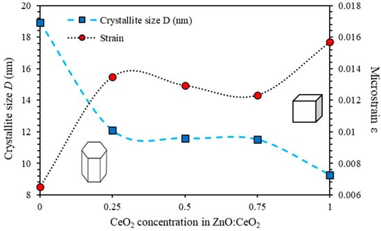
Figure 2.
The crystallite size, D and the microstrain ε of ZnO:CeO2 mixed oxides thin films as a function of CeO2 concentration calculated using Debye Scherrer’s equations.
Scherrer formula considers only the effect of crystallite size on the XRD peak broadening. However, it does not provide details of the intrinsic strain generated in the nanocomposites. It is induced by the point defect, grain boundary, triple junction and stacking faults [54,55]. There are many methods such as Williamsons Hall method (WH), Warren-Averbach method etc., which considers the effect of the strain induced by XRD peak broadening and can be used for the calculation of the intrinsic strain along with the particle size. Among these methods, Williamson–Hall (W–H) method which is considered to be easy, elegant and simple [56]. According to WH method, the line broadening of X-ray diffraction peak occurs due to the size and microstrain of the nanocrystals and the total broadening can be written as:
In the present work, average particle size and microstrain have been calculated using modified WH equation implementing Uniform deformation model (UDM). The method deliberately uses uniform strain all the way through the crystallographic direction that is induced in the nanocrystals due to crystal imperfections. In other words, UDM considers strain, which is isotropic in nature [57]. This intrinsic strain essentially affects the physical broadening of the XRD profile inducing peak broadening:
So, the total broadening due to strain and size in a particular peak indexed by hkl Miller indices, can be expressed as:
where, is the full width at half of the maximum intensity for different crystallographic diffraction planes. Consequently, WH equation is modified by UDM can be given by:
By plotting along Y-axis as a function of on the X-axis corresponding to each diffraction peak, we can calculate the values of crystallite size (D) and microstrain (ε). The estimated values of and of ZnO:CeO2 mixed oxide thin films are plotted as functions of CeO2 concentrations as shown in Figure 3. The peaks of ZnO; (100), (002), (101) and the peaks of CeO2; (111), (200), (220) and (311) are used in equation 6 to calculate D and ε. The value of D of pure ZnO and CeO2 thin films is estimated to be 28.05 nm and 8.10 nm, respectively. However, D of ZnO:CeO2 mixed oxide thin films containing 25%, 50% and 75% of CeO2 were found to be 25.89 nm, 19.85 nm and 12.12 nm, respectively. It can be seen that the calculated crystallite size of the ZnO:CeO2 mixed oxide thin films does not vary analytically with the Ce concentration. This could be attributed to the lattice disorder, produced in the powder samples at higher Ce concentrations due to the difference in the ionic radii of Zn2+ and Ce4+ species. Obviously, Figure 2 shows an inverse relationship between and D which could be attributed to the decrease in the volume occupied by the constituents inside the combined crystalline structure. In addition, as the volume of the unit cells increases, the total surface area is increased causing a shift in planes positions [53].
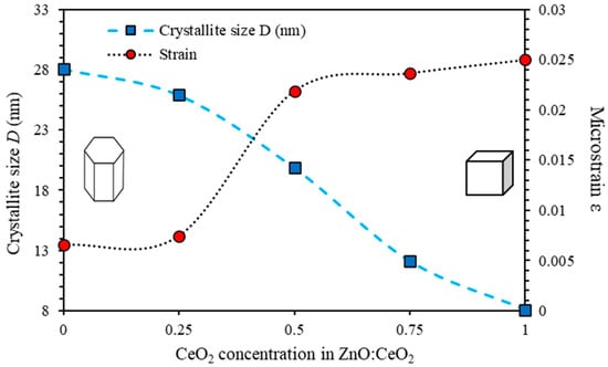
Figure 3.
The crystallite size, D and the microstrain ε of ZnO:CeO2 mixed oxides thin films as a function of CeO2 concentration calculated using Williamsons Hall equation.
Our results indicate that the values of the crystallite size using Scherrer method exhibit lower values than those obtained using WH method. However, the average microstrain, an inverse trend is obtained. The two methods differ from each other in the sense that WH method considers the effects of the broadening arise from the crystallite size and the microstrain. Whereas Scherrer method takes into account the broadening of the X-ray diffraction lines originates from the crystallite size only. Thus, Scherrer method considers the films as if they are a perfect system. Another major difference between the two methods lies in the fact that, WH method can be applied to analyze XRD patterns composed of of several diffraction lines, while in case of applying Scherrer method; it does not require more than one diffraction line. We conclude that, WH method is a general method and yields more accurate results than Scherrer method does.
To obtain a deeper insight into crystal defects, we investigate the dislocations that may be caused by internal stresses in the sub-lattices. Dislocations are formed at the boundaries between the glided and the un-slipped regions of the strained structure. The number per unit volume and the strength of dislocations determine the strength and ductility of materials. [58]. We calculate the density of dislocations (δ) by using the line profile analysis of XRD (LPA-XRD) patterns and using simple Williamson-Smallman formula given by , where is the crystallite size calculated using Williamsons Hall equation [48,58,59,60,61]. Figure 4a shows the dislocation density of the ZnO:CeO2 mixed oxides thin films as a function of CeO2 concentration. The value of of pure ZnO thin film is found to be lines/cm2 and that of pure CeO2 thin film is lines/cm2. The values of of ZnO:CeO2 mixed oxide thin films containing 25%, 50% and 75% of CeO2 are calculated to be and lines/cm2, respectively. The value of (δ) measures the agglomerations of crystalline clusters. The increasing (δ) with increasing the concentration of CeO2 in the mixed-oxide composite implies a decreasing of the crystallization and significant increasing of vacancies [58,60]. The increasing in dislocation density can be attributed to the internal strain during film formation in addition to the partial interstitial substitution of the Ce4+ ion instead of Zn2+.
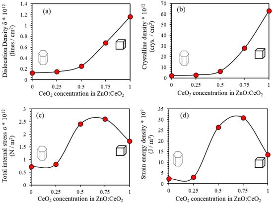
Figure 4.
(a) Dislocation density, (b) crystalline density, (c) total internal stress and (d) strain energy density of ZnO:CeO2 mixed oxides thin films as a function of CeO2 concentration.
The crystallites density (N) of thin films can be calculated from the estimated values of D and given by [62,63] where is the film thickness found to be 500 nm estimated using SEM micrograph. Figure 4b shows of ZnO:CeO2 mixed oxides thin films as a function of CeO2 concentration. The value of of pure ZnO thin film is found to be cryst./cm2 while for pure CeO2 thin film it exhibits a value of cryst./cm2. We found that exhibits values of and cryst./cm2 for ZnO:CeO2 mixed oxide thin films containing 25%, 50% and 75% of CeO2, respectively.
Temperature-induced lattice dynamical vibrations and mechanical-induced phase transitions and deformations are measured by the internal lattice stress. The value of the total internal stress () can be obtained from the linear region of stress-strain graph, where E is the Young’s Modulus (E). The value of of pure ZnO thin film is found to be N/m2 and that of pure CeO2 thin film is N/m2. For ZnO:CeO2 mixed oxide thin films containing 25%, 50% and 75% of CeO2, takes on values of 0.82 and cryst./cm2, respectively as displayed in Figure 4c. The strain energy density within thin films [] is closely related to Young’s modulus of the film, the volume of the unit cell and the internal micro strain . It can be expressed as [59,64]. The calculated value of of pure ZnO thin film is J/m3 and that of pure CeO2 thin film is J/m3. For ZnO:CeO2 mixed oxide thin films containing 25%, 50% and 75% of CeO2, is computed to be and N/m3, respectively, as shown in Figure 4d.
3.2. UV-Vis Spectroscopy Measurements of Optical Properties
Transmittance spectra of pure ZnO, pure CeO2 and ZnO:CeO2 mixed oxides thin films are displayed in Figure 5. Transmittance spectra of pure ZnO thin film show steep rising from about 0% up to 88% as wavelength increases from 300–350 nm. It maintains almost constant value for the 350–700 nm spectral range. Moreover, the transmittance spectra of pure CeO2 thin film demonstrate fast increasing trend about 0% up to 86% for the 300–420 nm spectral range. Similarly, it attains a constant value for 420–700 nm range. As can be clearly seen from Figure 5, transmittance of ZnO:CeO2 mixed oxides thin films have the same behavior of pure CeO2 thin film. However, it exhibits different transmittance values in 420–700 nm range. Interestingly, absorption edge is shifted towards the red region (lower energy) as CeO2 concentration in ZnO:CeO2 mixed oxides thin films is increased. Consequently, a considerable decrease in band gap energy is observed. To elucidate the significant reduction in the optical and gap energy, several factors are identified to contribute to this reduction. Among these is the fact that CeO2 thin films have lower band gap energy than ZnO thin films. In addition, enhanced fs-p interactions between the band electrons of ZnO:CeO2 mixed oxides and the localized fs electrons of cerium and the strong mismatch between the electronegativities of Ce and Zn in the ZnO: CeO2 mixed oxide system contribute significantly [65,66,67,68]. Small shoulders in transmittance spectra CeO2 and ZnO:CeO2 mixed oxides thin films appear at a wavelength of ~350 confirming the excitonic absorption characteristics of those thin films [69].
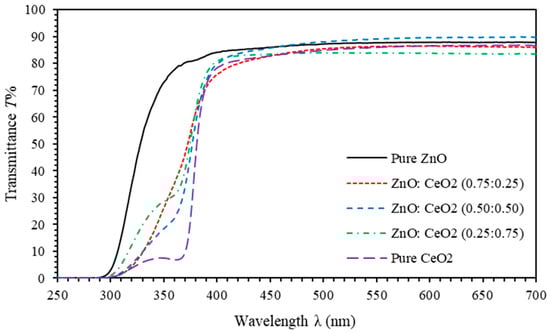
Figure 5.
Transmittance spectra of pure ZnO, pure CeO2 and ZnO:CeO2 mixed oxides thin films.
Reflectance spectra are shown in Figure 6. The reflectance values of pure ZnO and pure CeO2 thin film are found to be ranging from 5%–10% and 7%–15% as the wavelength decreases from 700 nm to 400 nm, respectively. Reflectance spectra of ZnO:CeO2 mixed oxides thin films demonstrate a tuning of as the concentration of CeO2 in ZnO:CeO2 mixed oxides is increased. This can be attributed to the changes in crystalline size and microstrain of ZnO:CeO2 mixed oxides crystals. In addition, ZnO:CeO2 mixed oxides thin films exhibit absorb photons of wavelength ranging between 280 nm to 330 nm efficiently. Consequently, incorporation of ZnO with CeO2 enhance UV–filter efficiency of thin films especially for UVB and UVC irradiation. Overall, ZnO:CeO2 mixed oxides thin films could be potential candidates for high transparency and UV-filter applications.
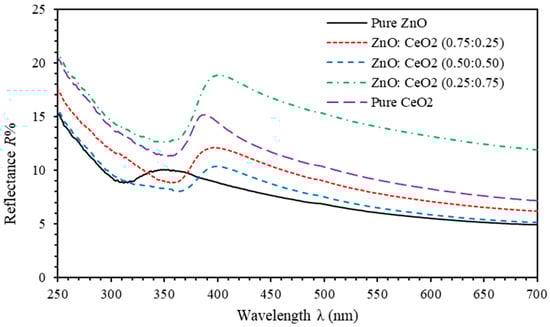
Figure 6.
Reflectance spectra of pure ZnO, pure CeO2 and ZnO:CeO2 mixed oxides thin films.
3.3. Analysis of Transmittance Spectra
Absorption coefficient ( describes the intensity attenuation of the electromagnetic waves passing through a thin film [70]. The parameter can be expressed using the corrected transmission (), as [2,71,72], where is the thickness of thin films measured using SEM micrograph and estimated to be 500 nm. Figure 7 shows the variation of of pure ZnO, pure CeO2 and ZnO:CeO2 mixed oxides thin films with the incident photon wavelength. Obviously, exhibits higher values just before the absorption edge compared with those after the absorption edge. This can be attributed to the resonance of the frequency of incident photons with that of electronic polarizability. The dramatic reduction of at the absorption edge could be explained in terms of the coupling occur between electrons of the constituents [73,74,75,76]. Furthermore, the red shift of absorption edge upon the introduction of CeO2 into ZnO:CeO2 mixed oxides thin films is due to the change in the width of localized states and consequent changes in the energy gap.
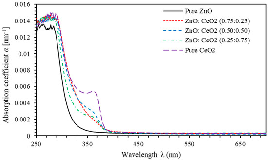
Figure 7.
Absorption coefficient spectra of pure ZnO, pure CeO2 and ZnO:CeO2 mixed oxides thin films.
To elucidate the attenuation of electromagnetic waves by the proposed thin films in this work, we calculate the extinction coefficient . It is related to the absorption coefficient, [2]. Figure 8 shows of pure ZnO, pure CeO2 and ZnO:CeO2 mixed oxides thin films as a function of incident photon wavelength. A drastic decrease of k is noticed prior to the absorption edge indicating that thin films allow electromagnetic waves to pass through without any decay or damping for . Moreover, k exhibits an increasing trend as the concentration of CeO2 introduced in ZnO:CeO2 mixed oxides thin films is increased. Therefore, ZnO:CeO2 mixed oxides thin films have a larger ability to attenuate incident light by scattering and absorption.
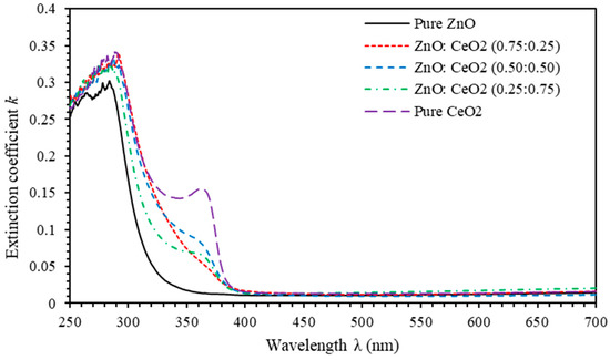
Figure 8.
The Extinction coefficient k spectra of pure ZnO, pure CeO2 and ZnO:CeO2 mixed oxides thin films.
The specific landscapes of the band structure and optical absorption edge of thin films can be simply interpreted by Tauc model [2]. The functional dependence of of pure ZnO, pure CeO2 and ZnO:CeO2 mixed oxides thin films versus photon energy is shown in Figure 9a. The optical band gaps obtained from Tauc plots are 3.296 eV for ZnO thin films and 3.092 eV for CeO2 thin films. The band gap energy decreases as 25% of CeO2 is introduced in ZnO:CeO2 mixed oxides thin films. A slight increase of the band gap is noticed as the concentration of CeO2 is further increased as shown in Figure 9b. We analyze the decrease in band gap and find that three factors contribute unequally to this decrease. Namely, CeO2 thin films exhibit lower band gap energy than ZnO thin films. Consequently, the increase of CeO2 content in the mixed oxide composites decreases the optical band gap. Furthermore, the strong ds-p interactions in ZnO:CeO2 mixed oxides and the large difference between the electronegativities of Ce and Zn in the ZnO:CeO2 mixed oxide system contribute to the optical band gap reduction [65,66,67,68]. Urbach energy, parameter can be used effectively to measure the degree of disorder in the thin films [75,77]. Near the optical band edge, absorption coefficient, , where is a constant, is the incident photon energy and is the Urbach energy. Urbach energy of ZnO thin film is found to be and that of CeO2 thin film is . For ZnO:CeO2 mixed oxides thin films, exhibits values intermediate between those of ZnO and CeO2 thin films. Figure 9c shows the variation of as a function of CeO2 concentration in ZnO:CeO2 mixed oxides thin films. We find that increases as concentration CeO2 is increased. For high CeO2 concentrations, attains nearly constant value. Furthermore, exhibits the lowest value for pure ZnO thin film indicating minimum disorder before introducing CeO2 consistent with the value of the microstrain calculated previously in XRD section. Interestingly, a direct relationship between and ε is observed as the concentration of CeO2 is increased. Linear fitting of the plots shows a direct relation between and ε as illustrated in Figure 9d. and ε follows the empirical relationship:
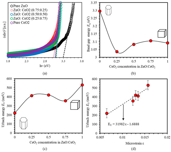
Figure 9.
(a) Tauc plot of pure ZnO, pure CeO2 and ZnO:CeO2 mixed oxides thin films, (b) Band gap energies () of ZnO:CeO2 mixed oxides thin films as a function of CeO2 concentrations, (c) Urbach energy () of pure ZnO, pure CeO2 and ZnO:CeO2 mixed oxides thin films and (d) Plot of the relationship between Urbach energy EU and microstrain ε of ZnO:CeO2 mixed oxides thin films.
3.4. Refractive Index Analysis
Refractive index, , of a thin film is closely related to electronic polarization of ions and the local electric and lattice fields [78,79]. The parameter can be expressed as [2]. Figure 10 shows of pure ZnO, pure CeO2 and ZnO:CeO2 mixed oxides thin films as a function of the wavelength of incident light. Obviously, spectral behavior of n can be divided into two regions. For () called anomalous dispersion region, the frequency of incident photon resonates with plasma frequency leading to strong electron coupling to the oscillating electric field [80]. For (normal dispersion region), n decreases continuously with increasing wavelength and shows significant normal dispersion. We found that n of ZnO and CeO2 thin films exhibits values ranging between 1.57 and 1.85 and 1.73 and 2.25 as the wavelength decreases from 700 nm to 400 nm, respectively. We found that increasing the concentration of CeO2 in ZnO:CeO2 mixed oxides thin films leads to considerable change of n values. This can be attributed to the changes induced in crystalline size and microstrain of ZnO:CeO2 mixed oxides crystals that leads to change in surface morphology and vacancies inside the crystal structure. High refractive index materials can be used in many optoelectronic applications such as enhancing the visual properties of electronic displays, which includes LCDs, OLEDs, and quantum dot (QDLED) televisions [81,82].
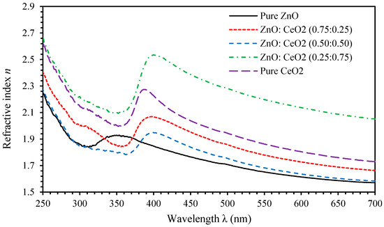
Figure 10.
The refractive index spectra of pure ZnO, pure CeO2 and ZnO:CeO2 mixed oxides thin films.
The dispersion of refractive index has been investigated intensively [83,84]. Wemple–DiDomenico (WDD) model is used to relate n with other key optical parameters such as effective single oscillator energy () and dispersion energy (). The model has been successful in estimating zero-frequency refractive index and zero-frequency dielectric constant () [12,85,86]. WDD model provides physical interpretation of the related optical parameters:
Therefore, plotting versus yields the values of the dispersion parameters via fitting the linear relation. Figure 11a shows versus for pure ZnO, pure CeO2 and ZnO:CeO2 mixed oxides thin films. The estimated values of and are presented in Table 2. The value of of pure ZnO and pure CeO2 thin films are found to be 3.959 eV and 3.603, respectively. The values of for ZnO:CeO2 mixed oxides thin films are found to be intermediate between those of pure ZnO and pure CeO2 thin films. Introducing CeO2 in ZnO:CeO2 mixed oxides thin films leads to a decrease in the energy of bonding and a change in the iconicity of these bonds in the nanocomposite. Consequently a decrease in the value of [76]. Moreover, the dispersion energy increases upon introducing CeO2 in ZnO:CeO2 mixed oxides. This increase could be attributed to the fact that cubic structure has higher dispersion energy than hexagonal structure. The values of and are used to estimate the zero-frequency dielectric constant and the zero-frequency refractive index by rewriting Equation (8) and setting leading to
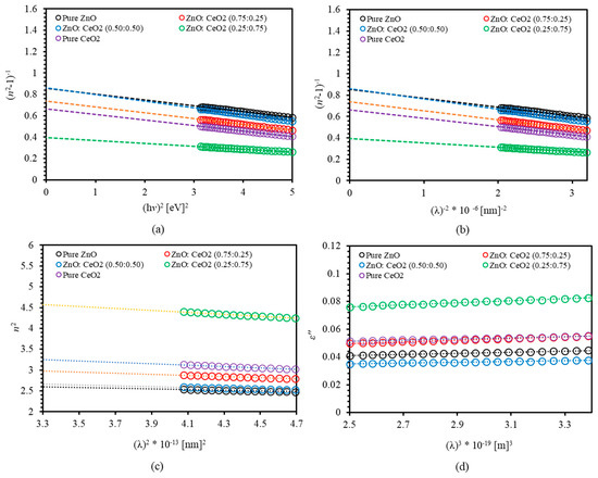
Figure 11.
(a) versus , (b) versus , (c) versus and (d) versus of pure ZnO, pure CeO2 and ZnO:CeO2 mixed oxides thin films.
Table 2.
Estimation of some essential optical parameters of the pure ZnO, pure CeO2, and ZnO:CeO2 thin films for various CeO2 concentrations.
The calculated values of are presented in Table 2. It is worth mentioning that the obtained values of are in good agreement with theoretical and the experimental values of the normal refractive index.
Sellmeier model is used to calculate the average oscillator wavelength and the oscillator length strength parameters [87]. According to this model,
Plotting against gives the oscillator parameters by fitting the linear relationship as demonstrated in Figure 11b. The values and are presented in Table 2. Our calculations indicate that increases as CeO2 introduces in ZnO:CeO2 mixed oxides. However, -value decreases as 25% and 50% of CeO2 are introduced in ZnO:CeO2 mixed oxides. Moreover, inserting 75% of CeO2 increases -value. This is due to the fact that is inversely proportional to whereas is directly proportional to . Obviously, introducing CeO2 into ZnO:CeO2 mixed oxides leads to an increase of and a decrease of , as a result of the decline of the surface morphology.
To elucidate the dielectric properties of mixed oxides thin film, the square of is correlated with the density of states ( and the high-frequency dielectric constant as formulated by Spitzer-Fan [88,89]:
where is the electronic charge, is the speed of light in vacuum, is the charge carrier density and is the effective mass of the carrier. Plotting versus is used to determine and . Figure 11c shows the dispersion nature of the index of refraction of our thin films. The estimated values of both and are listed in Table 2. The values of of pure ZnO and pure CeO2 thin films were found to be 2.868 and 3.801, respectively. The values of of ZnO:CeO2 mixed oxides thin films are found to increase upon increasing the concentration of CeO2 in ZnO:CeO2 mixed oxides thin films consistent with that of n [90,91]. We found that charge carrier density boosts upon increasing CeO2 content in ZnO:CeO2 mixed oxides thin films.
The imaginary part of the dielectric function () in relation to the wavelength of the incident photon could be analyzed to determine the relaxation time () defined by Drude free electron model [88]:
Figure 11d shows the variation of with for pure ZnO, pure CeO2 and ZnO:CeO2 mixed oxides thin films. The relaxation time could be determined from the slope of the plot between and , and from the value of calculated from Equation (7) taking [43].
4. Summary and Conclusions
In summary, synthesis, crystallography, microstructure, crystal defects, optical and optoelectronic characterization of ZnO:CeO2 mixed oxide-thin films dip-coated on glass substrates using a sol-gel technique are investigated and interpreted. Pure ZnO thin film is found to exhibit a hexagonal structure whereas that of pure CeO2 thin film is a fluorite cubic. XRD patterns demonstrate the formation of mixed oxide materials containing semi-crystalline nature from the constituent oxides. ZnO-CeO2 films were obtained with a hexagonal structure and extremely favored orientation with the c-axis perpendicular to glass substrates. The as-prepared mixed-oxide thin films exhibit several crystallographic orientations determined by the lattice mismatch between ZnO and CeO2 thin films and the concentration of added CeO2 thin films.
To elucidate deeper insight into crystal defects, we estimate the average microstrain and the crystallite size of pure ZnO and CeO2 thin films found to be 18.93 nm and 9.26 nm, respectively. In addition, we found that ZnO:CeO2 mixed oxide thin films containing 25%, 50% and 75% of CeO2 exhibit compositional-averaged crystallite sizes of 12.09 nm, 11.58 nm and 11.50 nm, respectively. Transmittance of all investigated thin films is found to attain high values of 85% in the visible region. Moreover, the refractive index of pure ZnO film was found to exhibit values ranging between 1.57 and 1.85, while that of CeO2 thin film take on values ranging between 1.73 and 2.25 as the wavelength decreases from 700 nm to 400 nm. Interestingly, ZnO:CeO2 mixed oxides thin films exhibit refractive indices that are strongly dependent on the content level of CeO2. We found a significant decrease of optical band gap as the concentration of CeO2 is increased in the mixed oxide thin films. Therefore, band gap engineering is achieved efficiently in this mixed oxide system.
The strong correlation among crystallinity, surface morphology and optical properties of the as-synthesized mixed oxide thin films is investigated and interpreted using XRD and UV-Vis spectroscopy. Different classical models such as WDD model, Sellmeier model, Spitzer-Fan model and Drude free electron model are employed to calculate and interpret the optoelectronic and dispersion properties of ZnO:CeO2 mixed oxides thin films. Obtaining mixed oxide thin films with controllable refractive index and tunable optical and optoelectronic properties provides a pathway to design smart multi-functional materials. Such materials may act as potential candidates for the fabrication of modern optoelectronic devices and thin film transistors.
Author Contributions
Conceptualization, Q.M.A.-B., A.M.A., A.A.A. and A.T.; methodology, Q.M.A.-B. and M.T.; software, H.B. and Z.C.; validation, A.A.A., A.T. and I.A.Q.; formal analysis, Q.M.A.-B. and A.M.A.; investigation, M.T.; resources, A.A.A.; data curation, A.M.A.; writing—original draft preparation, Q.M.A.-B.; writing—review and editing, A.A.A. and A.M.A.; visualization, A.T. and I.A.Q.; supervision, H.B. and Z.C.; project administration, A.A.A. All authors have read and agreed to the published version of the manuscript.
Funding
This research received no external funding.
Acknowledgments
The authors would like to acknowledge the deanship of scientific research at Jordan University of Science and Technology for its continuous financial and technical support. Our thanks also for Mohammad-Ali H. Al-Akhras for helping our members to use his biomedical laboratories and Borhan A. Elbiss for his technical support and valuable discussion.
Conflicts of Interest
The authors declare no conflict of interest.
References
- Al-Bataineh, Q.M.; Alsaad, A.; Ahmad, A.A.; Al-Sawalmih, A. Structural, Electronic and Optical Characterization of ZnO Thin Film-Seeded Platforms for ZnO Nanostructures: Sol–Gel Method Versus Ab Initio Calculations. J. Electron. Mater. 2019, 48, 5028–5038. [Google Scholar] [CrossRef]
- Ahmad, A.A.; Alsaad, A.M.; Al-Bataineh, Q.M.; Al-Naafa, M.A. Optical and structural investigations of dip-synthesized boron-doped ZnO-seeded platforms for ZnO nanostructures. Appl. Phys. A 2018, 124, 458. [Google Scholar] [CrossRef]
- Alsaad, A.; Ahmad, A.A.; Qattan, I.A.; AlBataineh, Z.; AlBataineh, Z. Structural, Optoelectrical, Linear, and Nonlinear Optical Characterizations of Dip-Synthesized Undoped ZnO and Group III Elements (B, Al, Ga, and In)-Doped ZnO Thin Films. Crystals 2020, 10, 252. [Google Scholar] [CrossRef]
- Ahmad, A.A.; Alsaad, Q.A.-B. Optical and structural characterization of dip synthesized Al-B Co-doped ZnO seeded platforms for ZnO nanostructures. Jordan J. Phys. 2017, 10, 33–48. [Google Scholar]
- Muchuweni, E.; Sathiaraj, T.; Nyakotyo, H. Synthesis and characterization of zinc oxide thin films for optoelectronic applications. Heliyon 2017, 3, e00285. [Google Scholar] [CrossRef]
- Malik, G.; Mourya, S.; Jaiswal, J.; Chandra, R. Effect of annealing parameters on optoelectronic properties of highly ordered ZnO thin films. Mater. Sci. Semicond. Process. 2019, 100, 200–213. [Google Scholar] [CrossRef]
- Sandeep, K.; Bhat, S.; Dharmaprakash, S. Structural, optical, and LED characteristics of ZnO and Al doped ZnO thin films. J. Phys. Chem. Solids 2017, 104, 36–44. [Google Scholar] [CrossRef]
- Kim, J.; Ji, J.-H.; Min, S.-W.; Jo, G.-H.; Jung, M.-W.; Park, M.-J.; Lee, S.-K.; Koh, J.-H. Enhanced conductance properties of UV laser/RTA annealed Al-doped ZnO thin films. Ceram. Int. 2017, 43, 3900–3904. [Google Scholar] [CrossRef]
- Kokate, S.K.; Jagtap, C.V.; Baviskar, P.K.; Jadkar, S.; Pathan, H.M.; Mohite, K.C. CdS sensitized cadmium doped ZnO solar cell: Fabrication and characterizations. Optik 2018, 157, 628–634. [Google Scholar] [CrossRef]
- Qiao, S.; Liu, J.; Fu, G.; Ren, K.; Li, Z.; Wang, S.; Pan, C. ZnO nanowire based CIGS solar cell and its efficiency enhancement by the piezo-phototronic effect. Nano Energy 2018, 49, 508–514. [Google Scholar] [CrossRef]
- Zhu, L.; Zeng, W. Room-temperature gas sensing of ZnO-based gas sensor: A review. Sens. Actuators A Phys. 2017, 267, 242–261. [Google Scholar] [CrossRef]
- Ahmad, A.A.; Al-Bataineh, Q.M.; Alsaad, A.M.; Samara, T.O.; Al-izzy, K.A. Optical properties of hydrophobic ZnO nano-structure based on antireflective coatings of ZnO/TiO2/SiO2 thin films. Phys. B Condens. Matter 2020, 593, 412263. [Google Scholar] [CrossRef]
- Khan, I.A.; Belkhedkar, M.R.; Salodkar, R.V.; Ubale, A.U. Physical properties of nanostructured CeO2 thin films grown by SILAR method. In Proceedings of the 2nd International Conference on Condensed Matter and Applied Physics (Icc 2017), Bikaner, India, 24–25 November 2017; AIP Publishing: Melville, NY, USA AIP Conference Proceedings 2018. ; Volume 1953, p. 030102. [Google Scholar]
- Kumar, P.; Kumar, P.; Kumar, A.; Sulania, I.; Chand, F.; Kandasami, A. Structural, optical and magnetic properties of N ion implanted CeO2 thin films. RSC Adv. 2017, 7, 9160–9168. [Google Scholar] [CrossRef]
- Jewariya, M.; Singh, P.; Moona, G.; Shanker, G.; Srivatsa, K.; Baek, I.H.; Jeong, Y.U. Investigation of dynamic optical behavior of CeO2 thin film using terahertz spectroscopy. Opt. Mater. 2018, 85, 295–297. [Google Scholar] [CrossRef]
- Zinzuvadiya, S.; Pandya, N.C.; Joshi, U.S. Optoelectronic response of (111) oriented CeO2 films for UV photodetector. Thin Solid Films 2019, 669, 525–530. [Google Scholar] [CrossRef]
- Tiwari, S.; Sen, S.; Shirage, P.M. Effect of Transition Elements Substitution on Structural, Optoelectronic, Magnetic and Mechanical Properties of CeO2. Ph.D. Thesis, IIT Indore, Indore, India, 2019. [Google Scholar]
- Miller, H.A.; Lavacchi, A.; Vizza, F.; Marelli, M.; Di Benedetto, F.; D’Acapito, F.; Paska, Y.; Page, M.; Dekel, D.R. A Pd/C-CeO2 Anode Catalyst for High-Performance Platinum-Free Anion Exchange Membrane Fuel Cells. Angew. Chem. Int. Ed. 2016, 55, 6004–6007. [Google Scholar] [CrossRef]
- Li, L.; Zhu, B.; Zhang, J.; Yan, C.; Wu, Y. Electrical properties of nanocube CeO2 in advanced solid oxide fuel cells. Int. J. Hydrog. Energy 2018, 43, 12909–12916. [Google Scholar] [CrossRef]
- Hadi, A.; Rashid, F.L.; Hussein, H.Q.; Hashim, A. Novel of water with (CeO2-WC) and (SiC-WC) nanoparticles systems for energy storage and release applications. In Proceedings of the IOP Conference Series: Materials Science and Engineering, Baghdad, Iraq, 6–7 March 2019; IOP Publishing; Volume 518, p. 032059. [Google Scholar]
- Sun, H.; Li, Y.; Yan, X.; Zhao, J.; Wang, Z. Thermochemical energy storage performance of Al2O3/CeO2 co-doped CaO-based material under high carbonation pressure. Appl. Energy 2020, 263, 114650. [Google Scholar] [CrossRef]
- Peng, R.; Li, S.; Sun, X.; Ren, Q.; Chen, L.; Fu, M.; Wu, J.; Ye, D. Size effect of Pt nanoparticles on the catalytic oxidation of toluene over Pt/CeO2 catalysts. Appl. Catal. B Environ. 2018, 220, 462–470. [Google Scholar] [CrossRef]
- Zhang, X.; Hou, F.; Yang, Y.; Wang, Y.; Liu, N.; Chen, D.; Yang, Y. A facile synthesis for cauliflower like CeO2 catalysts from Ce-BTC precursor and their catalytic performance for CO oxidation. Appl. Surf. Sci. 2017, 423, 771–779. [Google Scholar] [CrossRef]
- Gao, G.; Shi, J.W.; Liu, C.; Gao, C.; Fan, Z.; Niu, C. Mn/CeO2 catalysts for SCR of NOx with NH3: Comparative study on the effect of supports on low-temperature catalytic activity. Appl. Surf. Sci. 2017, 411, 338–346. [Google Scholar] [CrossRef]
- Lin, B.; Liu, Y.; Heng, L.; Wang, X.; Ni, J.; Lin, J.; Wang, X. Morphology Effect of Ceria on the Catalytic Performances of Ru/CeO2 Catalysts for Ammonia Synthesis. Ind. Eng. Chem. Res. 2018, 57, 9127–9135. [Google Scholar] [CrossRef]
- Ramezanzadeh, B.; Bahlakeh, G.; Ramezanzadeh, M. Polyaniline-cerium oxide (PAni-CeO2) coated graphene oxide for enhancement of epoxy coating corrosion protection performance on mild steel. Corros. Sci. 2018, 137, 111–126. [Google Scholar] [CrossRef]
- Li, B.; Zhang, W.; Li, D.; Wang, J. Electrodeposition of Ni W/ZrO2 nanocrystalline film reinforced by CeO2 nanoparticles: Structure, surface properties and corrosion resistance. Mater. Chem. Phys. 2019, 229, 495–507. [Google Scholar] [CrossRef]
- Torres-Huerta, A.; Domínguez-Crespo, M.; Brachetti-Sibaja, S.B.; Rosales, H.D.; Hernández-Pérez, M.; Lois-Correa, J.A. Preparation of ZnO:CeO2–x thin films by AP-MOCVD: Structural and optical properties. J. Solid State Chem. 2010, 183, 2205–2217. [Google Scholar] [CrossRef]
- Al-Kuhaili, M.; Durrani, S.; Bakhtiari, I.; Al-Kuhaili, M.F. Carbon monoxide gas-sensing properties of CeO2–ZnO thin films. Appl. Surf. Sci. 2008, 255, 3033–3039. [Google Scholar] [CrossRef]
- Qian, J.; Wang, Y.; Pan, J.; Chen, Z.; Wang, C.; Chen, J.; Wu, Z. Yangyue Non-enzymatic glucose sensor based on ZnO–CeO2 whiskers. Mater. Chem. Phys. 2020, 239, 122051. [Google Scholar] [CrossRef]
- Xiong, Z.; Lei, Z.; Xu, Z.; Chen, X.; Gong, B.; Zhao, Y.; Zhao, H.; Zhang, J.; Zheng, C. Flame spray pyrolysis synthesized ZnO/CeO2 nanocomposites for enhanced CO2 photocatalytic reduction under UV–Vis light irradiation. J. CO2 Util. 2017, 18, 53–61. [Google Scholar] [CrossRef]
- Liang, X.; Wang, P.; Gao, Y.; Huang, H.; Tong, F.; Zhang, Q.; Wang, Z.; Liu, Y.; Zheng, Z.; Dai, Y.; et al. Design and synthesis of porous M-ZnO/CeO2 microspheres as efficient plasmonic photocatalysts for nonpolar gaseous molecules oxidation: Insight into the role of oxygen vacancy defects and M=Ag, Au nanoparticles. Appl. Catal. B Environ. 2020, 260, 118151. [Google Scholar] [CrossRef]
- Ghouri, Z.K.; Barakat, N.A.; Kim, H.-Y.; Park, M.; Khalil, K.A.; El-Newehy, M.H.; Al-Deyab, S.S. Nano-engineered ZnO/CeO2 dots@CNFs for fuel cell application. Arab. J. Chem. 2016, 9, 219–228. [Google Scholar] [CrossRef]
- Nath, B.; Chaliha, C.; Kalita, E.; Kalita, M. Synthesis and characterization of ZnO:CeO2:nanocellulose:PANI bionanocomposite. A bimodal agent for arsenic adsorption and antibacterial action. Carbohydr. Polym. 2016, 148, 397–405. [Google Scholar] [CrossRef] [PubMed]
- Wang, D.Y.; Lin, Z.F.; Li, X.B.; Cheng, W.H.; Fu, Y.; Xu, L. Preparation and corrosion resistance of ZnO/CeO2 composite films. Surf. Eng. 2014, 32, 32–37. [Google Scholar] [CrossRef]
- Mueen, R.; Morlando, A.; Qutaish, H.; Lerch, M.; Cheng, Z.; Konstantinov, K. ZnO/CeO2 nanocomposite with low photocatalytic activity as efficient UV filters. J. Mater. Sci. 2020, 55, 6834–6847. [Google Scholar] [CrossRef]
- Kickelbick, G. The search of a homogeneously dispersed material—The art of handling the organic polymer/metal oxide interface. J. Sol-Gel Sci. Technol. 2008, 46, 281–290. [Google Scholar] [CrossRef]
- Mosley, D.W.; Auld, K.; Conner, D.; Gregory, J.; Liu, X.-Q.; Pedicini, A.; Thorsen, D.; Wills, M.; Khanarian, G.; Simon, E.S. High performance encapsulants for ultra high-brightness LEDs. SPIE Int. Soc. Opt. Eng. 2008, 6910, 691017. [Google Scholar]
- Allen, R.D.; Wallraff, G.M.; Hofer, D.C.; Kunz, R.R. Photoresists for 193-nm lithography. IBM J. Res. Dev. 1997, 41, 95–104. [Google Scholar] [CrossRef]
- Nakamura, T.; Fujii, H.; Juni, N.; Tsutsumi, N. Enhanced Coupling of Light from Organic Electroluminescent Device Using Diffusive Particle Dispersed High Refractive Index Resin Substrate. Opt. Rev. 2006, 13, 104–110. [Google Scholar] [CrossRef]
- Regolini, J.; Benoit, D.; Morin, P. Passivation issues in active pixel CMOS image sensors. Microelectron. Reliab. 2007, 47, 739–742. [Google Scholar] [CrossRef]
- Yang, S.; Zhang, Y. Structural and magnetic studies of Mn-doped CeO2 thin films prepared by sol-gel method. Integr. Ferroelectr. 2017, 185, 176–182. [Google Scholar] [CrossRef]
- Alsaad, A.; Ahmad, A.A.; Al-Bataineh, Q.M.; Bani-Salameh, A.A.; Abdullah, H.S.; Qattan, I.A.; AlBataineh, Z.; Telfah, A. Optical, Structural, and Crystal Defects Characterizations of Dip Synthesized (Fe-Ni) Co-Doped ZnO Thin Films. Materials 2020, 13, 1737. [Google Scholar] [CrossRef]
- Mishra, B.G.; Rao, G.R. Promoting effect of ceria on the physicochemical and catalytic properties of CeO2–ZnO composite oxide catalysts. J. Mol. Catal. A Chem. 2006, 243, 204–213. [Google Scholar] [CrossRef]
- Shechtman, D.; Blech, I.; Gratias, D.; Cahn, J.W. Metallic Phase with Long-Range Orientational Order and No Translational Symmetry. Phys. Rev. Lett. 1984, 53, 1951–1953. [Google Scholar] [CrossRef]
- Sarma, H.; Sarma, K. X-ray Peak Broadening Analysis of ZnO Nanoparticles Derived by Precipitation method. Int. J. Sci. Res. Publ. 2014, 4, 1–7. [Google Scholar]
- Kamakanth, K. Basics of X-ray Diffraction and Its Application; IK: New Delhi, India, 2007. [Google Scholar]
- Fu, D.-W.; Zhang, W.; Cai, H.-L.; Ge, J.-Z.; Zhang, Y.; Xiong, R.-G. Diisopropylammonium Chloride: A Ferroelectric Organic Salt with a High Phase Transition Temperature and Practical Utilization Level of Spontaneous Polarization. Adv. Mater. 2011, 23, 5658–5662. [Google Scholar] [CrossRef]
- Zak, A.K.; Majid, W.A.; Abrishami, M.E.; Yousefi, R. X-ray analysis of ZnO nanoparticles by Williamson–Hall and size–strain plot methods. Solid State Sci. 2011, 13, 251–256. [Google Scholar] [CrossRef]
- Shull, C.G. The Determination of X-ray Diffraction Line Widths. Phys. Rev. 1946, 70, 679–684. [Google Scholar] [CrossRef]
- Pielaszek, R. Diffraction Studies of Microstructure of Nanocrystals Exposed to High Pressure. Ph.D. Thesis, Warsaw University, Warsaw, Poland, 2003. [Google Scholar]
- Jona, F.; Shirane, G. Ferroelectric Crystals, International Series of Monographs on Solid State Physics; Pergamon Press: Oxford, UK, 1962. [Google Scholar]
- Horiuchi, S.; Tokunaga, Y.; Giovannetti, G.; Picozzi, S.; Itoh, H.; Shimano, R.; Kumai, R.; Tokura, Y. Above-room-temperature ferroelectricity in a single-component molecular crystal. Nat. Cell Biol. 2010, 463, 789–792. [Google Scholar] [CrossRef]
- Das, R.; Sarkar, S. Determination of intrinsic strain in poly (vinylpyrrolidone)-capped silver nano-hexapod using X-ray diffraction technique. Curr. Sci. 2015, 109, 775–778. [Google Scholar]
- Balzar, D.; Ledbetter, H. Voigt-function modeling in Fourier analysis of size- and strain-broadened X-ray diffraction peaks. J. Appl. Crystallogr. 1993, 26, 97–103. [Google Scholar] [CrossRef]
- Warren, B.E.; Averbach, B.L. The Separation of Cold-Work Distortion and Particle Size Broadening in X-ray Patterns. J. Appl. Phys. 1952, 23, 497. [Google Scholar] [CrossRef]
- Hall, W.H. X-ray Line Broadening in Metals. Proc. Phys. Soc. Sect. A 1949, 62, 741–743. [Google Scholar] [CrossRef]
- Akl, A.A.; Hassanien, A. Microstructure and crystal imperfections of nanosized CdSxSe1−x thermally evaporated thin films. Superlattices Microstruct. 2015, 85, 67–81. [Google Scholar] [CrossRef]
- Akl, A.; Mahmoud, S.A.; Al-Shomar, S.; Hassanien, A.S. Improving microstructural properties and minimizing crystal imperfections of nanocrystalline Cu2O thin films of different solution molarities for solar cell applications. Mater. Sci. Semicond. Process. 2018, 74, 183–192. [Google Scholar] [CrossRef]
- Williamson, G.K.; Smallman, R.E., III. Dislocation densities in some annealed and cold-worked metals from measurements on the X-ray debye-scherrer spectrum. Philos. Mag. 1956, 1, 34–46. [Google Scholar] [CrossRef]
- Fu, D.-W.; Cai, H.-L.; Liu, Y.; Ye, Q.; Zhang, W.; Zhang, Y.; Chen, X.-Y.; Giovannetti, G.; Capone, M.; Li, J.; et al. Diisopropylammonium Bromide Is a High-Temperature Molecular Ferroelectric Crystal. Scienve 2013, 339, 425–428. [Google Scholar] [CrossRef] [PubMed]
- Dawber, M.; Rabe, K.M.; Scott, J.F. Physics of thin-film ferroelectric oxides. Rev. Mod. Phys. 2005, 77, 1083–1130. [Google Scholar] [CrossRef]
- Scott, J.F. Applications of Modern Ferroelectrics. Science 2007, 315, 954–959. [Google Scholar] [CrossRef]
- Aly, K.; Khalil, N.; Algamal, Y.; Saleem, Q.M. Estimation of lattice strain for zirconia nano-particles based on Williamson- Hall analysis. Mater. Chem. Phys. 2017, 193, 182–188. [Google Scholar] [CrossRef]
- Goktas, A. High-quality solution-based Co and Cu co-doped ZnO nanocrystalline thin films: Comparison of the effects of air and argon annealing environments. J. Alloy. Compd. 2018, 735, 2038–2045. [Google Scholar] [CrossRef]
- Gungor, E.; Güngör, T.; Caliskan, D.; Ceylan, A.; Ozbay, E. Co doping induced structural and optical properties of sol–gel prepared ZnO thin films. Appl. Surf. Sci. 2014, 318, 309–313. [Google Scholar] [CrossRef]
- Samanta, K. Synthesis and Characterization of 3d-transation Metal Ions Doped ZnO Based Dilute Magnetic Semiconductor Thin Films. Ph.D. Thesis, Universidad de Puerto Rico, San Juan, Puerto Rico, 2009. [Google Scholar]
- Alsaad, A.; AlBataineh, Z.; Ahmad, A.; AlBataineh, Z.; Telfah, A. Optical band gap and refractive index dispersion parameters of boron-doped ZnO thin films: A novel derived mathematical model from the experimental transmission spectra. Optik 2020, 211, 164641. [Google Scholar] [CrossRef]
- Liu, Y.; Liu, Y.; Liu, Y.; Shen, D.; Lu, Y.; Zhang, J.; Fan, X. Structural and optical properties of nanocrystalline ZnO films grown by cathodic electrodeposition on Si substrates. Phys. B Condens. Matter 2002, 322, 31–36. [Google Scholar] [CrossRef]
- Atkins, P.W.; Jones, L.; Straushein, B. Chemistry: Molecules, Matter, and Change; WH Freeman: New York, NY, USA, 1997; Volume 354. [Google Scholar]
- Desiraju, G.; Steiner, T. The Weak Hydrogen Bond; Oxford University Press (OUP): Oxford, UK, 2001; Volume 9. [Google Scholar]
- Motohiro, N.; Hirota, M.; Umezawa, Y. The CH/p Interaction. Evidence, Nature, and Consequences; Wiley-VCH, Inc.: New York, NY, USA, 1998. [Google Scholar]
- Hassanien, A.; Akl, A.A. Effect of Se addition on optical and electrical properties of chalcogenide CdSSe thin films. Superlattices Microstruct. 2016, 89, 153–169. [Google Scholar] [CrossRef]
- Hassanien, A.S.; Akl, A.A. Optical characteristics of iron oxide thin films prepared by spray pyrolysis technique at different substrate temperatures. Appl. Phys. A 2018, 124, 752. [Google Scholar] [CrossRef]
- Urbach, F. The Long-Wavelength Edge of Photographic Sensitivity and of the Electronic Absorption of Solids. Phys. Rev. 1953, 92, 1324. [Google Scholar] [CrossRef]
- Hassanien, A.S.; Akl, A.A. Influence of composition on optical and dispersion parameters of thermally evaporated non-crystalline Cd50S50−xSex thin films. J. Alloys Compd. 2015, 648, 280–290. [Google Scholar] [CrossRef]
- Parmar, R.; Kundu, R.; Punia, R.; Aghamkar, P.; Kishore, N. Iron modified structural and optical spectral properties of bismuth silicate glasses. Phys. B Condens. Matter 2014, 450, 39–44. [Google Scholar] [CrossRef]
- Liu, J.-G.; Ueda, M. High refractive index polymers: Fundamental research and practical applications. J. Mater. Chem. 2009, 19, 8907–8919. [Google Scholar] [CrossRef]
- Duerloo, K.-A.N.; Ong, M.T.; Reed, E.J. Intrinsic Piezoelectricity in Two-Dimensional Materials. J. Phys. Chem. Lett. 2012, 3, 2871–2876. [Google Scholar] [CrossRef]
- Alsaad, A.; Marin, C.M.; Alaqtash, N.; Chao, H.-W.; Chang, T.-H.; Cheung, C.L.; Ahmad, A.; Qattan, I.; Sabirianov, R.F. Crystallographic, vibrational modes and optical properties data of α-DIPAB crystal. Data Brief 2018, 16, 667–684. [Google Scholar] [CrossRef]
- Yen, H.-J.; Liou, G.-S. A facile approach towards optically isotropic, colorless, and thermoplastic polyimidothioethers with high refractive index. J. Mater. Chem. 2010, 20, 4080–4084. [Google Scholar] [CrossRef]
- Macdonald, E.K.; Shaver, M.P. Intrinsic high refractive index polymers. Polym. Int. 2014, 64, 6–14. [Google Scholar] [CrossRef]
- Oriaku, C.; Osuwa, J.; Njoku, C. Single Oscillator Parameters and Optical Energies of Laser Irradiated Cu Doped Cds Thin Films. J. Non Oxide Glasses 2011, 3, 25–30. [Google Scholar]
- Hassanien, A.S.; Sharma, I. Optical properties of quaternary a-Ge15-x Sbx Se50 Te35 thermally evaporated thin-films: Refractive index dispersion and single oscillator parameters. Optik 2020, 200, 163415. [Google Scholar] [CrossRef]
- Sutcliffe, B.T.; Wilson, S. Potential energy curves and surfaces. Handb. Mol. Phys. Quantum Chem. 2003, 1, 574–587. [Google Scholar]
- Wemple, S.H.; DiDomenico, M. Behavior of the Electronic Dielectric Constant in Covalent and Ionic Materials. Phys. Rev. B 1971, 3, 1338–1351. [Google Scholar] [CrossRef]
- Patil, V.; Jundale, D.; Pawar, S.; Chougule, M.; Godse, P.; Patil, S.; Raut, B.; Sen, S.; Vikas, P.; Datta, J.; et al. Nanocrystalline CuO Thin Films for H2S Monitoring: Microstructural and Optoelectronic Characterization. J. Sens. Technol. 2011, 1, 36–46. [Google Scholar] [CrossRef]
- Fasasi, A.Y.; Osagie, E.; Pelemo, D.; Obiajunwa, E.; Ajenifuja, E.; Ajao, J.; Osinkolu, G.; Makinde, W.O.; Adeoye, A.E. Effect of Precursor Solvents on the Optical Properties of Copper Oxide Thin Films Deposited Using Spray Pyrolysis for Optoelectronic Applications. Am. J. Mater. Synth. Process. 2018, 3, 12. [Google Scholar] [CrossRef]
- Spitzer, W.G.; Fan, H.Y. Determination of Optical Constants and Carrier Effective Mass of Semiconductors. Phys. Rev. 1957, 106, 882–890. [Google Scholar] [CrossRef]
- Hassanien, A.S. Studies on dielectric properties, opto-electrical parameters and electronic polarizability of thermally evaporated amorphous Cd50S50−xSex thin films. J. Alloys Compd. 2016, 671, 566–578. [Google Scholar] [CrossRef]
- Farag, A.; Ashery, A.; Shenashen, M. Optical absorption and spectrophotometric studies on the optical constants and dielectric of poly (o-toluidine) (POT) films grown by spin coating deposition. Phys. B Condens. Matter 2012, 407, 2404–2411. [Google Scholar] [CrossRef]
Publisher’s Note: MDPI stays neutral with regard to jurisdictional claims in published maps and institutional affiliations. |
© 2020 by the authors. Licensee MDPI, Basel, Switzerland. This article is an open access article distributed under the terms and conditions of the Creative Commons Attribution (CC BY) license (http://creativecommons.org/licenses/by/4.0/).