Abstract
In this paper, an on chip two-dimensional Newton’s ring-like plasmonic sensor is designed for differentiating the chirality of circularly polarized lights (CPLS). The structure of the plasmonic sensor consists of a circular arc slit and an array of periodic rectangular nano-grooves that are etched into a silver film. When the sensor is illuminated by CPLS with a given chirality, the surface plasmon polariton waves generated by the slit and nano-groove array will selectively interfere with each other in the near field, which results in two different transmitted light intensity distributions in the far field. The generated far-field light intensity distributions are utilized as criteria to qualitatively differentiate the concrete chirality of the incident CPLS. The finite difference time domain method is utilized to theoretically investigate the function of the designed plasmonic sensor. The simulated results indicated that the proposed sensor has the ability to visually display the chirality information in the far field, and can provide a tool to conveniently and qualitatively differentiate the chirality of CPLS in the far field.
1. Introduction
Analyzing the specific chirality of circularly polarized lights (CPLS) is of great importance in applications such as the analysis of the physiological properties of chiral molecules and polarization imaging techniques [1]. Polarization-sensitive plasmonic devices have been realized by specifically designing artificial metal micro- or nanostructures [2,3,4,5,6,7,8,9,10,11,12,13,14,15]. By the interaction of circularly polarized light and the plasmonic structure, a chirality-dependent plasmonic sensor can be realized. When the sensor is incident by CPLS with different chirality, different patterns of surface plasmon polaritons (SPP)-based light intensity distributions are generated in the near field. SPPs are one kind of two-dimensional surface waves that propagate along the interface between metal and dielectric [16,17,18]. The generated near-field light intensity distributions have been used to differentiate the chirality of the incident CPLS [19,20,21,22,23,24,25,26,27,28,29]. However, these sensors have some limitations in practical applications. For example, in order to obtain the near-field SPP-based light intensity distributions, a time consuming and expensive near-field optical scanning microscope is usually needed.
To solve this problem, one effective solution is to convert the SPP-based near-field light intensity distributions to the far-field light intensity distribution for detection purposes [30]. There are already some chirality-dependent plasmonic devices that can generate different far-field light intensity distributions [5,31,32]. Theoretically, the structures designed in these references can be used as chirality sensors for differentiating the concrete chirality of the incident CPLS. In ref. [33], our group proposed a SPP interference-based plasmonic sensor that can quantitatively differentiate the chirality of the incident CPLS. Through Fourier transform of the obtained SPP-interference-modulated far-field interference fringes, the chirality of the incident CPLS is quantitatively differentiated by the frequency value of the interference fringes obtained in the far field. On the contrary, the purpose and significance of this paper is to provide a qualitative scheme to differentiate the chirality of CPLS in the far field.
In this paper, an on chip two-dimensional Newton’s ring-like plasmonic structure suitable for differentiating the chirality of the CPLS is theoretically designed and numerically investigated. The proposed plasmonic sensor mainly consists of a circular arc slit and an array of periodic rectangular nano-grooves, which are both etched into a thin silver film. The working principle of the designed sensor is to modulate the far-field light intensity distribution transmitted through the sensor by the near-field SPP waves interference. The function of the designed plasmonic sensor is theoretically investigated by using the finite difference time domain method. The simulated results show that, when the sensor is illuminated by CPLS with a given chirality, the SPP waves generated by the slit and nano-groove array will selectively interfere with each other in the near field, leading to two different transmitted light intensity distributions in the far field. Then, the generated far-field light intensity distributions can be utilized as criteria to qualitatively differentiate the concrete chirality of the incident CPLS. The proposed plasmonic sensor has the ability to visually display the chirality information in the far field, providing a tool to conveniently and qualitatively differentiate the chirality of CPLS in the far field.
2. Structure and Methods
Figure 1a shows the structure diagram of the designed plasmonic sensor at the x-y plane. The designed sensor comprises an array of spatially arranged periodic rectangular nanogrooves (named ‘G’) and a micron length circular arc slit (named ‘S’), which are both etched into a silver film with thickness of 150 nm. The two parallel columns of rectangular nanogrooves are perpendicular to each other [10]. The length, width and height of a single rectangular nanogroove are 200 nm, 40 nm and 120 nm, respectively. The spacing between two adjacent rectangular nanogrooves along the x-axis and y-axis is Δx = 0.153 μm, Δy = 0.2 μm. As the length of the circular arc slit along y direction is about 15 um, each column has about 75 rectangular grooves. The width and height of the circular arc slit are 100 nm and 150 nm. The outer radius and inner radius of the circular arc slit are Rout = 16 μm and Rinner = 15.9 μm. The center angle of the circular arc slit is θ = 40°. The minimum and maximum spacing between the right boundary of the ‘G’ and the left boundary of the ‘S’ are dmin = 0.9 μm and dmax = 1.9 μm, respectively. Figure 1b shows the schematic diagram of the optical path that was used to test the sensing function of the device. Figure 1b shows the test light path that can be selected in the actual experimental operation. a collimated CPL plane wave normally illuminates the plasmonic sensor. The transmitted far-field light intensity distributions can be collected and magnified by an objective lens with high numerical aperture, and then imaged by a CCD camera.
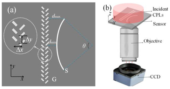
Figure 1.
(a) Structure diagram of the designed plasmonic sensor at x−y plane, two parallel columns of spatially arranged rectangular nanogrooves (named ‘G’) and a micron length circular arc slit (named ‘S’) are etched into a thin silver film with thickness of 150 nm, Δx = 0.153 μm, Δy = 0.2 μm, dmin = 0.9 μm, dmax = 1.9 μm, θ = 40°. (b) Schematic diagram of a reference functional testing optical path for detecting the chirality of the incident CPLs in the actual experiment.
The commercial software Lumerical finite difference time domain solutions is utilized to numerically investigate the function of the designed plasmonic sensor. In the simulations, a perfectly matched layer-absorbing boundary condition is utilized to efficiently terminate the outer boundary of the computational region. The amplitude of the incident light is set to 1. Thus, all the results given in this paper are the normalized electric field light intensity distributions generated by the designed plasmonic sensor. The wavelength of the incident CPL is λo = 633 nm. As the dielectric permittivity of the silver at 633 nm is ε = −15.9317 + i1.07633, the corresponding wavelength of the generated SPP waves is λspp = 0.6128 μm. Thus, we can calculate that, dmin ≈ 1.47λspp, dmax ≈ 3.09λspp.
The function of the designed sensor is jointly determined by the structures of ‘G’ and the ‘S’. The structure of the ‘G’ is sensitive to the chiral characteristics of the incident CPLS, and has the function of directionally launching SPP waves [10]. Specifically, when the structure of the ‘G’ is normally illuminated by a left-handed CPL, the SPP wave generated by the ‘G’ can only propagate to the left along the metal surface (negative direction of x-axis). However, when the ‘G’ is normally illuminated by a right-handed CPL, the SPP wave generated by the ‘G’ can only propagate to the right along the metal surface. This function has also been proved in detail by our group [4,33]. On the contrary, the structure of the ‘S’ is not sensitive to the chiral characteristics of the incident CPLS. That is, whether the incident light is left-handed CPL or right-handed CPL, the SPP waves can be excited on both sides of the circular arc slit. Parts of the SPP waves generated by the circular arc slit will converge towards the center of the circular arc slit.
The different chirality responses of the structures of ‘G’ and ‘S’ to the incident CPLS make it feasible for us to design the plasmonic sensor in this paper. On the one hand, when the incident light is a collimated left-handed CPL, the SPP plane wave generated by structure ‘G’ and the SPP wave generated by structure ‘S’ will not meet on the metal surface. Thus, there will be no interference at the position of the ‘S’. At this time, the transmitted field of the ‘S’ is only determined by itself, which will form a convergent light intensity distribution. On the other hand, when the incident light is a collimated right-handed CPL, the SPP plane wave generated by the ‘G’ will propagate toward the ‘S’, and meets the SPP wave generated by ‘S’ at the position of the ‘S’, resulting in SPP interference-based near-field light intensity distributions. In this instance, the transmitted field of the sensor is modulated by ‘G’ and ‘S’ together. In short, when the designed sensor is illuminated by a collimated CPLS with different chirality, two different near-field light intensity distributions can be generated by the designed plasmonic sensor. Then, the generated SPP-based near-field light field will be reconverted back to the free space photons through the circular arc slit ‘S’ [34,35], resulting in two different transmitted far-field light intensity distributions, which here are utilized as criteria to qualitatively differentiate the chirality information of the incident CPLS.
3. Results
Figure 2 shows the simulated results of the normalized electric field light intensity distributions generated by the designed plasmonic sensor. In the simulation, the amplitude of the incident light is set to 1. Figure 2a–c presents the simulated results when the incident light is a collimated right-handed CPL. Figure 2d–f corresponds to the simulated results when the incident light is a collimated left handed CPL. Figure 2a,d shows the near-field light intensity distributions at a distance of zo = −200 nm from the bottom of the silver film. Figure 2b,e shows the far-field light intensity distributions at a distance of zo = −6 μm from the bottom of the silver film. As we know, the maximum penetration depth of SPPS in the dielectric is generally less than one wavelength. Hence, the distance zo ≥ 10λspp can be regarded as the far field. In this paper, zo = −6 μm is approximately equal to 10λspp. Figure 2c shows the electric field light intensity distribution at y-z plane (i.e., x = 0 μm, −6 μm ≤ z ≤ −0.3 μm) for the case of Figure 2a,b. Figure 2f shows the electric field light intensity distribution at y-z plane (i.e., x = 0 μm, −6 μm ≤ z ≤ −0.3 μm) for the case of Figure 2d,e.
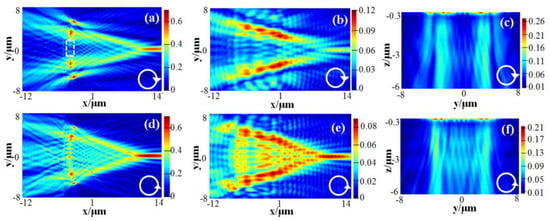
Figure 2.
The simulated results of the (a) near field at zo = −200 nm and (b) far field at zo = −6 μm electric field light intensity distributions generated by the sensor for the case of right−hand CPL incidence. The simulated results of the (d) near field at zo = −200 nm and (e) far field at zo = −6 μm electric field light intensity distributions for the case of of left−hand CPL incidence. (c,f) show the electric field light intensity distribution at y−z plane (i.e., x = 0 μm, −6 μm ≤ z ≤ −0.3 μm) of the cases of (a,b) and (d,e), respectively. The amplitude of the incident light is set to 1.
As demonstrated in Figure 2, no matter in the near field or far field, two different types of light intensity distributions can be generated. Under the illumination of right-hand CPL, the light intensity distributions similar to ‘2D hollow cone’ are generated (see Figure 2a,b). Figure 2c shows this ‘2D hollow cone’ light field distribution more intuitively at the y-z plane. As the light field propagates in the negative z direction, there is always a hollow (or dark) light field in the central region of the light field. In contrast, under the illumination of left-hand CPL, the light intensity distributions similar to ‘2D solid cone’ are generated (see Figure 2d,e). Figure 2f also shows this ‘2D solid cone’ light field distribution more intuitively at the y-z plane. As the light field propagates toward the negative z axis, there is always a solid (or bright) light field in the central area of the light field. The reason for the formation of such ‘2D hollow cone’-type light intensity distributions can be explained by means of the formation principle of 3D Newton’s ring interference fringes. According to the conditions for the formation of dark rings in Newton’s rings, the following formula can be used to explain why a ‘2D hollow cone’-type light intensity distribution can be formed: d = (k + 0.5)λspp, in which d is the spacing between the right boundary of the ‘G’ and the left boundary of the ‘S’, dmin = 0.9 μm and dmax = 1.9 μm, λspp = 0.6128 μm and k indicates the interference order. As mentioned in Section 2, dmin ≈ 1.47λspp and dmax ≈ 3.09λspp. It can be deduced that the values of k are k = 1 (i.e., d = 1.5 ∗ 0.6128 = 1 μm) and k = 2 (i.e., d = 2.5 ∗ 0.6128 = 1.5 μm). That is, two dark bands can be generated at the position of the ‘S’. Among them, d = 1.5 ∗ 0.6128 = 1 μm corresponds to the first order dark bands given in the white rectangular dashed frame shown in Figure 2a. The interference weakening phenomenon occurs here. Thus, weak intensity at the center of arc ‘S’ is generated in the transmitted field, which is called ‘2D hollow cone’-type light intensity distribution. According to the forming conditions of bright rings in 3D Newton’s rings, i.e., d = k’λspp, it can be deduced that the values of k’ are k’ = 2 (i.e., d = 2 ∗ 0.6128 = 1.2 μm) and k’ = 3 (i.e., d = 3 ∗ 0.6128 = 1.8 μm). That is, two bright bands can also be generated at the position of the ‘S’. The two dark bands and two bright bands can be seen from Figure 2a. As we know, Newton’s ring is a three-dimensional light field composed of a series of bright and dark rings. Figure 2a,b can be seen as a cut plane of the three-dimensional Newton’s rings (i.e., they make a cut plane along a certain diameter of the Newton’s ring). From Figure 2a–c, it can be clearly seen that there are two dark bands and two bright bands. Thus, these theoretical explanations are in perfect agreement with the simulated results.
In contrast, under the illumination of left-hand CPL, the light intensity distributions similar to ‘2D solid cone’ are generated, see Figure 2d–f. At this time, the generated SPP plane waves by the structure ‘G’ can only propagate to the left along the metal surface, which will not meet the SPP waves generated by the structure ‘S’. The transmitted light field of the structure ‘S’ will not be affected and modulated by the SPP plane waves generated by the structure ‘G’. The transmitted light intensity distribution of the designed sensor is a convergent light intensity distribution on the x-y plane, which is only determined by the circular arc slit itself.
4. Discussion
The influences of the center angle θ and the radius R of the ‘S’ on the transmitted electric field light intensity distributions are discussed in detail, when the incident light is a collimated right-handed CPL.
Figure 3 shows the results of the influences of center angle θ of the ‘S’ on the transmitted electric field light intensity distributions for the cases of (a)(b)θ = 30° and (d)(e) θ = 56°. In the simulation experiment, all structural parameters and simulation parameters involved in the results of Figure 2 remain unchanged, except for the center angle θ of the ‘S’. The change of the center angle θ will only lead to the change of the maximum spacing dmax, which denotes the maximum spacing between the right boundary of the ‘G’ and the left boundary of the ‘S’. The amplitude of the incident light is set to 1. Figure 3c shows the electric field light intensity distribution at the y-z plane (i.e., x = 0μm, −6 μm ≤ z ≤ −0.3 μm) for the case of Figure 3a,b. Figure 3f shows the electric field light intensity distribution at the y-z plane (i.e., x = 0μm, −6 μm ≤ z ≤ −0.3 μm) for the case of Figure 3d,e. Figure 3a,d corresponds to near-field light intensity distributions at zo = −200 nm. Figure 3b,e corresponds to far-field light intensity distributions at zo = −6 μm. As mentioned earlier, Figure 2a–c shows the simulated results of the near-field and far-field light intensity distributions generated by the designed plasmonic sensor, when the incident light is a collimated right-handed CPL, for the case of the center angle of θ = 40°.
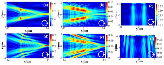
Figure 3.
The simulated results for the influence of the center angle of circular arc slit on the transmitted electric field light intensity distributions for the case of (a,b) θ = 30°, (d,e) θ = 56°. The plasmonic sensor is illuminated by right−handed CPL. (a,d) correspond to near field at zo = −200 nm, (b,e) correspond to far field at zo = −6 μm. (c,f) show the electric field light intensity distribution at y-z plane (i.e., x = 0 μm, −6 μm ≤ z ≤ −0.3 μm) for the cases of (a,b) and (d,e), respectively. The amplitude of the incident light is set to 1.
It can be seen from Figure 3 and Figure 2a–c that, the larger the central angle θ is, the more interference orders k are included in the light intensity distributions, and the greater the number of corresponding bright or dark bands. At the same time, with the increase of the center angle θ and the interference orders k, the intensity value of the transmitted light field of the slit will also increase. It can be seen from Figure 2c and Figure 3c,f that the dark area of the corresponding ‘2D hollow cone’ is not changed as the central angle θ increases, as the distance of the dmin remains unchanged.
The influences of the radius R of the ‘S’ on the transmitted electric field light intensity distributions are also discussed, when the incident light is a collimated right-handed CPL. Figure 4 shows the simulated results of the influence of the radius R of the ‘S’ on the transmitted light intensity distributions for the cases of (a)(d) Rout = 9 μm, (b)(e) Rout = 16 μm and (c)(f) Rout = 21 μm. Among them, (a)(b)(c) denote the simulated results for right-handed CPL incidence; (d)(e)(f) denote the simulated results for left-handed CPL incidence. In Figure 4, only the simulated results of the near-field light intensity distributions are given. The corresponding simulated results of the far-field light intensity distributions are not given, as they have the same characteristics as the near field. In the simulation experiment, the central angles corresponding to the three circular arc slits with different radii are equal, that is, θ = 40°. The minimum spacing between the right edge of ‘G’ and the left edge of ‘S’ also remains unchanged, which is dmin = 0.9 μm. Therefore, when the radius R of the ‘S’ changes, the position of the center of the circular arc slit will simultaneously change. It can be seen from Figure 4a–c that, for the case of right-handed CPL incidence, the larger the radius R is, the more interference orders k are included in the light intensity distributions. At the same time, the larger the radius R is, the larger the dark area of the corresponding ‘2D hollow cone’. Hence, in order to increase the dark area of the ‘2D hollow cone’, the radius of the circular arc slit can be appropriately increased. In contrast, it can be seen from Figure 4d–f that, for the case of left-handed CPL incidence, the larger the radius R is, the larger the area of the ‘2D solid cone’. A concentrated light field intensity distribution will always be formed.
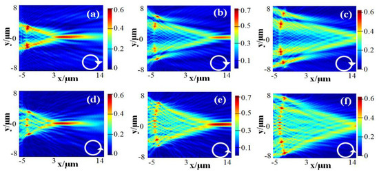
Figure 4.
The simulated results of influences of the radius R of the ‘S’ on the near field electric field light intensity distributions zo = −200 nm for the cases of (a,d) Rout = 9μm, (b,e) Rout = 16μm and (c,f) Rout = 21μm. (a–c) for the simulated results of right−handed CPL incidence. (d−f) for the simulated results of left−handed CPL incidence. The amplitude of the incident light is set to 1.
5. Conclusions
In conclusion, a two-dimensional Newton’s ring-like plasmonic sensor, which consists of a circular arc slit and an array of periodic rectangular nano-grooves that are etched into a silver film, is designed for differentiating the chirality of CPLS. To realize the function of this planar plasmonic sensor on the chip manipulation of the SPPS, interference is of crucial importance. The generated far-field light intensity distribution is modulated by SPPS interference-based light intensity distributions in the near field.
The finite difference time domain method is performed to simulate the function of the designed plasmonic sensor. The simulated results show that, when the sensor is illuminated by the CPLS with different chirality, two different types of the SPPS interference-modulated light intensity distributions can be formed in the far field. For instance, when the sensor is illuminated by a right-handed CPL, the sensor can form a light intensity distribution similar to a ‘2D hollow cone’. When the sensor is illuminated by a left-handed CPL, the sensor can form a light intensity distribution similar to a ‘2D solid cone’. These two far-field light intensity distributions are completely different. The chirality information of the incident CPLS is hidden in the far-field light intensity distributions, and can be conveniently inferred from these two different light intensity distributions. Thus, direct visualization of the chirality information of the incident CPLS can be achieved in the far field.
In the end, the obtained results indicated that the proposed sensor can provide a tool to conveniently and qualitatively differentiate the chirality of CPLS in the far field. This is the main motivation for developing this plasmonic sensor in this paper.
Author Contributions
Conceptualization, L.Z. and P.Q.; methodology, P.Q.; validation, L.Z.; formal analysis, C.B.; investigation, D.Z.; resources and data curation, T.P. and X.Z; writing—original draft preparation, L.Z.; writing—review and editing, C.B.; visualization, X.Z.; supervision, P.Q.; project administration, Y.X.; funding acquisition, X.Z. All authors have read and agreed to the published version of the manuscript.
Funding
This research was funded by the National Natural Science Foundation of China (12047568, and 12147219), the Natural Science Foundation of Zhejiang Province, China (LQ21B030004) and the Scientific Research Fund of Zhejiang Provincial Education Department, China (Y202146019).
Institutional Review Board Statement
Not applicable.
Informed Consent Statement
Not applicable.
Data Availability Statement
The data presented in this study are available from the corresponding author upon request.
Conflicts of Interest
The authors declare no conflict of interest.
References
- Zhang, J.; Guo, Z.; Zhou, K.; Ran, L.; Zhu, L.; Wang, W.; Sun, Y.; Shen, F.; Gao, J.; Liu, S. Circular polarization analyzer based on an Archimedean nano-pinholes array. Opt. Express 2015, 23, 30523–30531. [Google Scholar] [CrossRef] [PubMed]
- Zhang, Y.B.; Liu, H.; Cheng, H.; Tian, J.G.; Chen, S.Q. Multi-dimensional manipulation of wave fields based on artificial microstructures. Opto-Electron. Adv. 2020, 3, 200002. [Google Scholar] [CrossRef]
- Wang, S.; Wang, S.; Zhang, Y. Simultaneous airy beam generation for both surface plasmon polaritons and transmitted wave based on metasurface. Opt. Express 2017, 25, 23589–23596. [Google Scholar] [CrossRef] [PubMed]
- Qiu, P.Z.; Lv, T.G.; Zhang, Y.P.; Yu, B.B.; Lian, J.Q.; Jing, M.; Zhang, D.W. Polarization controllable device for simultaneous generation of surface plasmon polariton bessel-like beams and bottle beams. Nanomaterials 2018, 8, 975. [Google Scholar] [CrossRef] [PubMed]
- Wang, Y.; Zhao, P.; Feng, X.; Xu, Y.; Liu, F.; Cui, K.; Zhang, W.; Huang, Y. Dynamically sculpturing plasmonic vortices: From integer to fractional orbital angular momentum. Sci. Rep. 2016, 6, 36269. [Google Scholar] [CrossRef] [PubMed]
- Garoli, D.; Zilio, P.; Gorodetski, Y.; Tantussi, F.; De Angelis, F. Optical vortex beam generator at nanoscale level. Sci. Rep. 2016, 6, 29547. [Google Scholar] [CrossRef]
- Song, E.Y.; Lee, S.Y.; Hong, J.; Lee, K.; Lee, Y.; Lee, G.Y.; Kim, H.; Lee, B. A double-lined metasurface for plasmonic complex-field generation. Laser Photonics Rev. 2016, 10, 299–306. [Google Scholar] [CrossRef]
- Lee, S.Y.; Kim, K.; Lee, G.Y.; Lee, B. Polarization-multiplexed plasmonic phase generation with distributed nanoslits. Opt. Express 2015, 23, 15598–15607. [Google Scholar] [CrossRef]
- Lee, S.Y.; Kim, K.; Kim, S.J.; Park, H.; Kim, K.Y.; Lee, B. Plasmonic meta-slit: Shaping and controlling near-field focus. Optica 2015, 2, 6–13. [Google Scholar] [CrossRef]
- Lin, J.; Mueller, J.P.B.; Wang, Q.; Yuan, G.; Antoniou, N.; Yuan, X.C.; Capasso, F. Polarization-controlled tunable directional coupling of surface plasmon polaritons. Science 2013, 340, 331–334. [Google Scholar] [CrossRef]
- Bachman, K.A.; Peltzer, J.J.; Flammer, P.D.; Furtak, T.E.; Collins, R.T.; Hollingsworth, R.E. Spiral plasmonic nanoantennas as circular polarization transmission filters. Opt. Express 2012, 20, 1308–1319. [Google Scholar] [CrossRef]
- Ziegler, J.I.; Haglund, R.F. Plasmonic response of nanoscale spirals. Nano Lett. 2010, 10, 3013–3018. [Google Scholar] [CrossRef] [PubMed]
- Gorodetski, Y.; Niv, A.; Kleiner, V.; Hasman, E. Observation of the spin-based plasmonic effect in nanoscale structures. Phys. Rev. Lett. 2008, 101, 043903. [Google Scholar] [CrossRef] [PubMed]
- Afshinmanesh, F.; White, J.S.; Cai, W.; Brongersma, M.L. Measurement of the polarization state of light using an integrated plasmonic polarimeter. Nanophotonics 2012, 1, 125–129. [Google Scholar] [CrossRef]
- Zaman, M.A.; Hesselink, L. Dynamically controllable plasmonic tweezers using C-shaped nano-engravings. Appl. Phys. Lett. 2022, 121, 181108. [Google Scholar] [CrossRef] [PubMed]
- Barnes, W.L.; Dereux, A.; Ebbesen, T.W. Surface plasmon subwavelength optics. Nature 2003, 424, 824–830. [Google Scholar] [CrossRef]
- Ozbay, E. Plasmonics: Merging photonics and electronics at nanoscale dimensions. Science 2006, 311, 189–193. [Google Scholar] [CrossRef]
- Feng, J.; Li, D.; Pacifici, D. Circular slit-groove plasmonic interferometers: A generalized approach to high-throughput biochemical sensing [invited]. Opt. Mater. Express 2015, 5, 2742–2753. [Google Scholar] [CrossRef]
- Zhou, H.; Su, S.; Ma, H.; Zhao, Z.; Lin, Z.; Qiu, W.; Qiu, P.; Huang, B.; Kan, Q. Chiral graphene plasmonic archimedes’ spiral nanostructure with tunable circular dichroism and enhanced sensing performance. Opt. Express 2020, 28, 31954–31966. [Google Scholar] [CrossRef]
- Zhu, B.; Ren, G.; Gao, Y.; Wu, B.; Wan, C.; Jian, S. Graphene circular polarization analyzer based on spiral metal triangle antennas arrays. Opt. Express 2015, 23, 24730–24737. [Google Scholar] [CrossRef]
- Zhu, B.; Ren, G.; Gao, Y.; Wu, B.; Wan, C.; Jian, S. Graphene circular polarization analyzer based on unidirectional excitation of plasmons. Opt. Express 2015, 23, 32420–32428. [Google Scholar] [CrossRef]
- Zhu, B.; Ren, G.; Cryan, M.J.; Wan, C.; Gao, Y.; Yang, Y.; Jian, S. Tunable graphene-coated spiral dielectric lens as a circular polarization analyzer. Opt. Express 2015, 23, 8348–8356. [Google Scholar] [CrossRef] [PubMed]
- Zhang, J.; Guo, Z.; Li, R.; Wang, W.; Zhang, A.; Liu, J.; Qu, S.; Gao, J. Circular polarization analyzer based on the combined coaxial Archimedes’ spiral structure. Plasmonics 2015, 10, 1255–1261. [Google Scholar] [CrossRef]
- Li, J.; Tang, P.; Liu, W.; Huang, T.; Wang, J.; Wang, Y.; Lin, F.; Fang, Z.; Zhu, X. Plasmonic circular polarization analyzer formed by unidirectionally controlling surface plasmon propagation. Appl. Phys. Lett. 2015, 106, 161106. [Google Scholar] [CrossRef]
- Li, R.; Guo, Z.; Wang, W.; Zhang, J.; Zhang, A.; Liu, J.; Qu, S.; Gao, J. Ultra-thin circular polarization analyzer based on the metal rectangular split-ring resonators. Opt. Express 2014, 22, 27968–27975. [Google Scholar] [CrossRef]
- Chen, W.; Nelson, R.L.; Zhan, Q. Efficient miniature circular polarization analyzer design using hybrid spiral plasmonic lens. Opt. Lett. 2012, 37, 1442–1444. [Google Scholar] [CrossRef] [PubMed]
- Zhi, W.; Chen, W.; Abeysinghe, D.C.; Nelson, R.L.; Zhan, Q. Two-photon fluorescence characterization of spiral plasmonic lenses as circular polarization analyzers. Opt. Lett. 2010, 35, 1755–1757. [Google Scholar] [CrossRef]
- Chen, W.; Abeysinghe, D.C.; Nelson, R.L.; Zhan, Q. Experimental confirmation of miniature spiral plasmonic lens as a circular polarization analyzer. Nano Lett. 2010, 10, 2075–2079. [Google Scholar] [CrossRef]
- Yang, S.; Chen, W.; Nelson, R.L.; Zhan, Q. Miniature circular polarization analyzer with spiral plasmonic lens. Opt. Lett. 2009, 34, 3047–3049. [Google Scholar] [CrossRef]
- Wang, S.; Wang, X.; Kan, Q.; Qu, S.; Zhang, Y. Circular polarization analyzer with polarization tunable focusing of surface plasmon polaritons. Appl. Phys. Lett. 2015, 107, 243504. [Google Scholar] [CrossRef]
- Guo, W.P.; Liang, W.Y.; Cheng, C.W.; Wu, W.L.; Wang, Y.T.; Sun, Q.; Zu, S.; Misawa, H.; Cheng, P.J.; Chang, S.W.; et al. Chiral second-harmonic generation from monolayer WS2/Aluminum plasmonic vortex metalens. Nano lett. 2020, 20, 2857–2864. [Google Scholar] [CrossRef] [PubMed]
- Gorodetski, Y.; Drezet, A.; Genet, C.; Ebbesen, T.W. Generating far-field orbital angular momenta from near-field optical chirality. Phys. Rev. Lett. 2013, 110, 203906. [Google Scholar] [CrossRef]
- Qiu, P.Z.; Bai, C.Y.; Mao, Y.H.; Zhang, D.W. Circular polarization analyzer based on surface plasmon polariton interference. Opt. Express 2021, 29, 37907–37916. [Google Scholar] [CrossRef] [PubMed]
- Yavas, O.; Kocabas, C. Plasmon interferometers for high-throughput sensing. Opt. Lett. 2012, 37, 3396–3398. [Google Scholar] [CrossRef]
- Uulu, D.A.; Ashirov, T.; Polat, N.; Yakar, O.; Balci, S.; Kocabas, C. Fourier transform plasmon resonance spectrometer using nanoslit-nanowire pair. Appl. Phys. Lett. 2019, 114, 251101. [Google Scholar] [CrossRef]
Disclaimer/Publisher’s Note: The statements, opinions and data contained in all publications are solely those of the individual author(s) and contributor(s) and not of MDPI and/or the editor(s). MDPI and/or the editor(s) disclaim responsibility for any injury to people or property resulting from any ideas, methods, instructions or products referred to in the content. |
© 2023 by the authors. Licensee MDPI, Basel, Switzerland. This article is an open access article distributed under the terms and conditions of the Creative Commons Attribution (CC BY) license (https://creativecommons.org/licenses/by/4.0/).